Product
Folder
Order
Now
Support &
Community
Tools &
Software
Technical
Documents
CSD19531KCS
ZHCSBK8C – SEPTEMBER 2013 – REVISED MARCH 2017
CSD19531KCS 100V N 通道 NexFET™功
功率金属氧化物半导体场效应晶体
管 (MOSFET)
1 特性
•
•
•
•
•
•
•
1
产品概要
超低 Qg 和 Qgd
低热阻
雪崩额定值
无铅引脚镀层
符合 RoHS 环保标准
无卤素
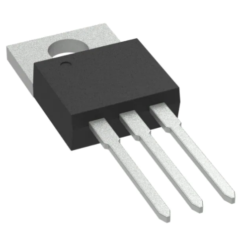
晶体管 (TO)-220 塑料封装
典型值
TA=25°C
漏源电压
100
V
Qg
栅极电荷总量 (10V)
37
nC
Qgd
栅极电荷(栅极到漏极)
RDS(on)
漏源导通电阻
VGS(th)
阈值电压
7.5
nC
VGS = 6V
7.3
VGS = 10V
6.4
2.7
mΩ
V
器件信息(1)
2 应用范围
•
•
•
单位
VDS
次级侧同步整流器
热插拔电信应用
电机控制
器件
封装
包装介
质
数量
运输
CSD19531KCS
TO-220 塑料封装
管
50
管
(1) 要了解所有可用封装,请见数据表末尾的可订购产品附录。
绝对最大额定值
3 说明
此 100V、6.4mΩ、TO-220 NexFET™功率 MOSFET
被设计成在功率转换应用中大大降低 损耗。
值
单位
VDS
漏源电压
100
V
VGS
栅源电压
±20
V
持续漏极电流(受封装限制)
100
持续漏极电流(受芯片限制),TC = 25°C 时
测得
110
持续漏极电流(受芯片限制),TC = 100°C
时测得
78
TA=25°C
.
Drain (Pin 2)
ID
Gate
(Pin 1)
(1)
A
IDM
脉冲漏极电流
285
A
PD
功率耗散
214
W
TJ,
Tstg
工作结温,
储存温度
-55 至 175
°C
EAS
雪崩能量,单一脉冲
ID = 60A,L = 0.1mH,RG = 25Ω
180
mJ
Source (Pin 3)
(1) 最大 RθJC = 0.7ºC/W,脉冲持续时间 ≤ 100μs,占空比 ≤ 1%。
RDS(on) 与 VGS 间的关系
栅极电荷
10
TC = 25°C, I D = 60A
TC = 125°C, I D = 60A
18
VGS - Gate-to-Source Voltage (V)
RDS(on) - On-State Resistance (mΩ)
20
16
14
12
10
8
6
4
2
0
0
2
4
6
8
10
12
14
16
VGS - Gate-to- Source Voltage (V)
18
20
G001
ID = 60A
VDS = 50V
9
8
7
6
5
4
3
2
1
0
0
4
8
12
16
20
24
28
Qg - Gate Charge (nC)
32
36
40
G001
1
An IMPORTANT NOTICE at the end of this data sheet addresses availability, warranty, changes, use in safety-critical applications,
intellectual property matters and other important disclaimers. PRODUCTION DATA.
English Data Sheet: SLPS407
�CSD19531KCS
ZHCSBK8C – SEPTEMBER 2013 – REVISED MARCH 2017
www.ti.com.cn
目录
1
2
3
4
5
特性 ..........................................................................
应用范围...................................................................
说明 ..........................................................................
修订历史记录 ...........................................................
Specifications.........................................................
1
1
1
2
3
5.1 Electrical Characteristics........................................... 3
5.2 Thermal Information .................................................. 3
5.3 Typical MOSFET Characteristics.............................. 4
6
器件和文档支持 ........................................................ 7
6.1
6.2
6.3
6.4
6.5
7
接收文档更新通知 .....................................................
社区资源....................................................................
商标 ...........................................................................
静电放电警告.............................................................
Glossary ....................................................................
7
7
7
7
7
机械、封装和可订购信息 ......................................... 8
7.1 KCS 封装尺寸 ........................................................... 8
4 修订历史记录
Changes from Revision B (June 2014) to Revision C
Page
•
已添加 接收文档更新通知部分和社区资源部分至器件和文档支持部分................................................................................... 7
•
已更改 KCS 封装尺寸部分中的封装图 .................................................................................................................................... 8
Changes from Revision A (May 2014) to Revision B
•
Page
Added value for max Qg ......................................................................................................................................................... 3
Changes from Original (September 2013) to Revision A
Page
•
已将芯片限制电流更新为反映器件运行温度范围内的增加量 .................................................................................................. 1
•
已增加脉冲电流来反映全新条件 ............................................................................................................................................. 1
•
已增加最大功率耗散来反映全新条件 ...................................................................................................................................... 1
•
已将运行温度范围和结温范围增加至 175ºC .......................................................................................................................... 1
•
更新了脉冲漏极电流条件 ........................................................................................................................................................ 1
•
Changed Figure 1 from a normalized RθJA curve to a normalized RθJC curve ....................................................................... 4
•
Updated Figure 6 to reflect increase in device operating temperature range ....................................................................... 5
•
Updated Figure 8 to reflect increase in device operating temperature range ....................................................................... 5
•
Updated Figure 10 to reflect measured SOA data ................................................................................................................ 6
•
Updated Figure 12 to reflect increase in device operating temperature range ..................................................................... 6
2
版权 © 2013–2017, Texas Instruments Incorporated
�CSD19531KCS
www.ti.com.cn
ZHCSBK8C – SEPTEMBER 2013 – REVISED MARCH 2017
5 Specifications
5.1 Electrical Characteristics
TA = 25°C (unless otherwise stated)
PARAMETER
TEST CONDITIONS
MIN
TYP
MAX
UNIT
STATIC CHARACTERISTICS
BVDSS
Drain-to-source voltage
VGS = 0 V, ID = 250 μA
IDSS
Drain-to-source leakage current
VGS = 0 V, VDS = 80 V
1
μA
IGSS
Gate-to-source leakage current
VDS = 0 V, VGS = 20 V
100
nA
VGS(th)
Gate-to-source threshold voltage
VDS = VGS, ID = 250 μA
V
RDS(on)
Drain-to-source on resistance
gfs
Transconductance
100
2.2
V
2.7
3.3
VGS = 6 V, ID = 60 A
7.3
8.8
VGS = 10 V, ID = 60 A
6.4
7.7
VDS = 10 V, ID = 60 A
137
mΩ
S
DYNAMIC CHARACTERISTICS
Ciss
Input capacitance
Coss
Output capacitance
Crss
Reverse transfer capacitance
RG
Series gate resistance
Qg
Gate charge total (10 V)
38
Qgd
Gate charge gate-to-drain
Qgs
Gate charge gate-to-source
Qg(th)
Gate charge at Vth
Qoss
Output charge
td(on)
Turnon delay time
tr
Rise Time
7.2
ns
td(off)
Turnoff delay time
16
ns
tf
Fall time
4.1
ns
VGS = 0 V, VDS = 50 V, ƒ = 1 MHz
VDS = 50 V, ID = 60 A
VDS = 50 V, VGS = 0 V
VDS = 50 V, VGS = 10 V,
IDS = 60 A, RG = 0 Ω
2980
3870
pF
560
728
pF
13
17
pF
1.3
2.6
Ω
49
nC
7.5
nC
11.9
nC
7.3
nC
98
nC
8.4
ns
DIODE CHARACTERISTICS
VSD
Diode forward voltage
ISD = 60 A, VGS = 0 V
0.9
1
V
Qrr
Reverse recovery charge
nC
Reverse recovery time
VDS= 50 V, IF = 60 A,
di/dt = 300 A/μs
270
trr
83
ns
5.2 Thermal Information
TA = 25°C (unless otherwise stated)
MAX
UNIT
RθJC
Junction-to-case thermal resistance
THERMAL METRIC
0.7
°C/W
RθJA
Junction-to-ambient thermal resistance
62
°C/W
Copyright © 2013–2017, Texas Instruments Incorporated
MIN
TYP
3
�CSD19531KCS
ZHCSBK8C – SEPTEMBER 2013 – REVISED MARCH 2017
www.ti.com.cn
5.3 Typical MOSFET Characteristics
TA = 25°C (unless otherwise stated)
200
200
180
180
160
140
120
100
80
60
VGS =10V
VGS =8V
VGS =6V
40
20
0
0
0.4
0.8
1.2
1.6
VDS - Drain-to-Source Voltage (V)
Figure 2. Saturation Characteristics
4
IDS - Drain-to-Source Current (A)
IDS - Drain-to-Source Current (A)
Figure 1. Transient Thermal Impedance
2
G001
VDS = 5V
160
140
120
100
80
60
TC = 125°C
TC = 25°C
TC = −55°C
40
20
0
0
1
2
3
4
5
6
VGS - Gate-to-Source Voltage (V)
7
8
G001
Figure 3. Transfer Characteristics
Copyright © 2013–2017, Texas Instruments Incorporated
�CSD19531KCS
www.ti.com.cn
ZHCSBK8C – SEPTEMBER 2013 – REVISED MARCH 2017
Typical MOSFET Characteristics (continued)
TA = 25°C (unless otherwise stated)
100000
Ciss = Cgd + Cgs
Coss = Cds + Cgd
Crss = Cgd
ID = 60A
VDS = 50V
9
8
10000
C − Capacitance (pF)
VGS - Gate-to-Source Voltage (V)
10
7
6
5
4
3
1000
100
10
2
1
0
0
4
8
12
16
20
24
28
Qg - Gate Charge (nC)
32
36
1
40
0
10
20
G001
Figure 4. Gate Charge
ID = 250uA
3.1
2.9
2.7
2.5
2.3
2.1
1.9
1.7
1.3
−75 −50 −25
RDS(on) - On-State Resistance (mΩ)
VGS(th) - Threshold Voltage (V)
100
G001
20
1.5
Figure 6. Threshold Voltage vs Temperature
TC = 25°C, I D = 60A
TC = 125°C, I D = 60A
18
16
14
12
10
8
6
4
2
0
0
25 50 75 100 125 150 175 200
TC - Case Temperature (ºC)
G001
0
2
4
6
8
10
12
14
16
VGS - Gate-to- Source Voltage (V)
18
20
G001
Figure 7. On-State Resistance vs Gate-to-Source Voltage
100
2.4
VGS = 6V
VGS = 10V
ISD − Source-to-Drain Current (A)
Normalized On-State Resistance
90
Figure 5. Capacitance
3.3
2.2
30
40
50
60
70
80
VDS - Drain-to-Source Voltage (V)
2
1.8
1.6
1.4
1.2
1
0.8
0.6
0.4
−75 −50 −25
TC = 25°C
TC = 125°C
10
1
0.1
0.01
0.001
ID = 60A
0
25 50 75 100 125 150 175 200
TC - Case Temperature (ºC)
G001
Figure 8. Normalized On-State Resistance vs Temperature
Copyright © 2013–2017, Texas Instruments Incorporated
0.0001
0
0.2
0.4
0.6
0.8
VSD − Source-to-Drain Voltage (V)
1
G001
Figure 9. Typical Diode Forward Voltage
5
�CSD19531KCS
ZHCSBK8C – SEPTEMBER 2013 – REVISED MARCH 2017
www.ti.com.cn
Typical MOSFET Characteristics (continued)
TA = 25°C (unless otherwise stated)
1000
100
10us
100us
1ms
10ms
DC
100
10
1
Single Pulse
Max RthetaJC = 0.7ºC/W
0.1
0.1
TC = 25ºC
TC = 125ºC
IAV - Peak Avalanche Current (A)
IDS - Drain-to-Source Current (A)
5000
1
10
100
VDS - Drain-to-Source Voltage (V)
1000
G001
Figure 10. Maximum Safe Operating Area
10
0.01
0.1
TAV - Time in Avalanche (mS)
1
G001
Figure 11. Single Pulse Unclamped Inductive Switching
IDS - Drain- to- Source Current (A)
125
100
75
50
25
0
−50 −25
0
25
50
75 100 125 150 175 200
TC - Case Temperature (ºC)
G001
Figure 12. Maximum Drain Current vs Temperature
6
版权 © 2013–2017, Texas Instruments Incorporated
�CSD19531KCS
www.ti.com.cn
ZHCSBK8C – SEPTEMBER 2013 – REVISED MARCH 2017
6 器件和文档支持
6.1 接收文档更新通知
如需接收文档更新通知,请访问 www.ti.com.cn 网站上的器件产品文件夹。点击右上角的提醒我 (Alert me) 注册
后,即可每周定期收到已更改的产品信息。有关更改的详细信息,请查阅已修订文档中包含的修订历史记录。
6.2 社区资源
The following links connect to TI community resources. Linked contents are provided "AS IS" by the respective
contributors. They do not constitute TI specifications and do not necessarily reflect TI's views; see TI's Terms of
Use.
TI E2E™ Online Community TI's Engineer-to-Engineer (E2E) Community. Created to foster collaboration
among engineers. At e2e.ti.com, you can ask questions, share knowledge, explore ideas and help
solve problems with fellow engineers.
Design Support TI's Design Support Quickly find helpful E2E forums along with design support tools and
contact information for technical support.
6.3 商标
NexFET, E2E are trademarks of Texas Instruments.
All other trademarks are the property of their respective owners.
6.4 静电放电警告
这些装置包含有限的内置 ESD 保护。 存储或装卸时,应将导线一起截短或将装置放置于导电泡棉中,以防止 MOS 门极遭受静电损
伤。
6.5 Glossary
SLYZ022 — TI Glossary.
This glossary lists and explains terms, acronyms, and definitions.
版权 © 2013–2017, Texas Instruments Incorporated
7
�CSD19531KCS
ZHCSBK8C – SEPTEMBER 2013 – REVISED MARCH 2017
www.ti.com.cn
7 机械、封装和可订购信息
以下页中包括机械、封装和可订购信息。这些信息是针对指定器件可提供的最新数据。这些数据会在无通知且不对
本文档进行修订的情况下发生改变。要获得这份数据表的浏览器版本,请查阅左侧的导航栏。
7.1 KCS 封装尺寸
4.7
4.4
10.36
9.96
1.32
1.22
2.9
2.6
6.5
6.1
8.55
8.15
(6.3)
( 3.84)
12.5
12.1
19.65 MAX
9.25
9.05
3X
3.9 MAX
13.12
12.70
3
1
3X
0.47
0.34
0.90
0.77
2.79
2.59
2X 2.54
3X
1.36
1.23
5.08
4222214/A 10/2015
注释:
1. 所有控制线性尺寸的单位均为英寸。括号中的尺寸单位均为毫米。括号或括弧中的尺寸均仅供参考。尺寸和容
限值遵循 ASME Y14.5M。
2. 本图纸如有变更,恕不通知。
3. 参考 JEDEC 注册 TO-220。
表 1. 引脚配置
8
位置
名称
引脚 1
栅极
引脚 2 / 标签
漏极
引脚 3
源极
版权 © 2013–2017, Texas Instruments Incorporated
�PACKAGE OPTION ADDENDUM
www.ti.com
10-Dec-2020
PACKAGING INFORMATION
Orderable Device
Status
(1)
Package Type Package Pins Package
Drawing
Qty
Eco Plan
(2)
Lead finish/
Ball material
MSL Peak Temp
Op Temp (°C)
(3)
Device Marking
(4/5)
(6)
CSD19531KCS
ACTIVE
TO-220
KCS
3
50
RoHS-Exempt
& Green
SN
N / A for Pkg Type
-55 to 175
CSD19531KCS
(1)
The marketing status values are defined as follows:
ACTIVE: Product device recommended for new designs.
LIFEBUY: TI has announced that the device will be discontinued, and a lifetime-buy period is in effect.
NRND: Not recommended for new designs. Device is in production to support existing customers, but TI does not recommend using this part in a new design.
PREVIEW: Device has been announced but is not in production. Samples may or may not be available.
OBSOLETE: TI has discontinued the production of the device.
(2)
RoHS: TI defines "RoHS" to mean semiconductor products that are compliant with the current EU RoHS requirements for all 10 RoHS substances, including the requirement that RoHS substance
do not exceed 0.1% by weight in homogeneous materials. Where designed to be soldered at high temperatures, "RoHS" products are suitable for use in specified lead-free processes. TI may
reference these types of products as "Pb-Free".
RoHS Exempt: TI defines "RoHS Exempt" to mean products that contain lead but are compliant with EU RoHS pursuant to a specific EU RoHS exemption.
Green: TI defines "Green" to mean the content of Chlorine (Cl) and Bromine (Br) based flame retardants meet JS709B low halogen requirements of
很抱歉,暂时无法提供与“CSD19531KCS”相匹配的价格&库存,您可以联系我们找货
免费人工找货- 国内价格
- 1+18.48960
- 10+16.36200
- 50+15.27120
- 国内价格 香港价格
- 1+21.547081+2.79110
- 3+19.366203+2.50860
- 10+15.6150910+2.02270
- 25+12.5618625+1.62720
- 50+10.6426950+1.37860
- 100+10.38098100+1.34470