Sample &
Buy
Product
Folder
Support &
Community
Tools &
Software
Technical
Documents
CSD88537ND
SLPS455A – JANUARY 2014 – REVISED AUGUST 2014
CSD88537ND Dual 60-V N-Channel NexFET™ Power MOSFET
1 Features
•
•
•
•
•
1
Product Summary
Ultra-Low Qg and Qgd
Avalanche Rated
Pb Free
RoHS Compliant
Halogen Free
TA = 25°C
2 Applications
•
•
TYPICAL VALUE
Drain-to-Source Voltage
60
V
Qg
Gate Charge Total (10 V)
14
nC
Qgd
Gate Charge Gate-to-Drain
RDS(on)
Drain-to-Source On-Resistance
VGS(th)
Threshold Voltage
Half Bridge for Motor Control
Synchronous Buck Converter
This dual SO-8, 60 V, 12.5 mΩ NexFET™ power
MOSFET is designed to serve as a half bridge in low
current motor control applications.
2
G1
3
S2
4
G2
nC
15
mΩ
VGS = 10 V
12.5
mΩ
3.0
V
Device
Media
Qty
Package
Ship
CSD88537ND
13-Inch Reel
2500
CSD88537NDT
7-Inch Reel
250
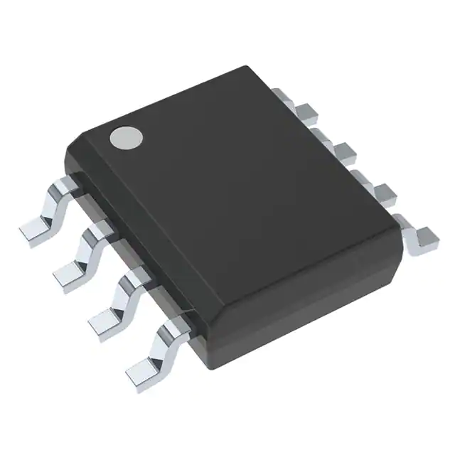
SO-8 Plastic
Package
Tape and
Reel
(1) For all available packages, see the orderable addendum at
the end of the data sheet.
Top View
1
2.3
VGS = 6 V
.
Ordering Information(1)
3 Description
S1
UNIT
VDS
Absolute Maximum Ratings
8
7
6
5
TA = 25°C
D1
VALUE
UNIT
VDS
Drain-to-Source Voltage
60
V
VGS
Gate-to-Source Voltage
±20
V
Continuous Drain Current (Package limited)
15
Continuous Drain Current (Silicon limited),
TC = 25°C
16
D1
ID
D2
Continuous Drain Current
D2
(1)
A
8.0
IDM
Pulsed Drain Current, TA = 25°C(2)
108
A
PD
Power Dissipation(1)
2.1
W
.
TJ,
Tstg
Operating Junction and
Storage Temperature Range
–55 to 150
°C
.
EAS
Avalanche Energy, single pulse
ID = 32, L = 0.1 mH, RG = 25 Ω
51
mJ
.
(1) Typical RθJA = 60°C/W on a 1-inch2, 2-oz. Cu pad on a
0.06-inch thick FR4 PCB.
(2) Max RθJL = 20°C/W, pulse duration ≤100 μs, duty cycle ≤1%
.
RDS(on) vs VGS
Gate Charge
10
TC = 25°C, I D = 8A
TC = 125°C, I D = 8A
27
VGS - Gate-to-Source Voltage (V)
RDS(on) - On-State Resistance (mΩ)
30
24
21
18
15
12
9
6
3
0
0
2
4
6
8
10
12
14
16
VGS - Gate-to- Source Voltage (V)
18
20
G001
ID = 8A
VDS = 30V
9
8
7
6
5
4
3
2
1
0
0
3
6
9
Qg - Gate Charge (nC)
12
15
G001
1
An IMPORTANT NOTICE at the end of this data sheet addresses availability, warranty, changes, use in safety-critical applications,
intellectual property matters and other important disclaimers. PRODUCTION DATA.
�CSD88537ND
SLPS455A – JANUARY 2014 – REVISED AUGUST 2014
www.ti.com
Table of Contents
1
2
3
4
5
Features ..................................................................
Applications ...........................................................
Description .............................................................
Revision History.....................................................
Specifications.........................................................
1
1
1
2
3
5.1 Electrical Characteristics........................................... 3
5.2 Thermal Information .................................................. 3
5.3 Typical MOSFET Characteristics.............................. 4
6
Device and Documentation Support.................... 7
6.1 Trademarks ............................................................... 7
6.2 Electrostatic Discharge Caution ................................ 7
6.3 Glossary .................................................................... 7
7
Mechanical, Packaging, and Orderable
Information ............................................................. 8
7.1 SO-8 Package Dimensions....................................... 8
7.2 Recommended PCB Pattern and Stencil Opening ... 9
4 Revision History
Changes from Original (January 2014) to Revision A
Page
•
Pulsed drain current increased from 62 to 108 A .................................................................................................................. 1
•
Updated pulsed drain current conditions ................................................................................................................................ 1
•
Changed RθJC to RθJL in Thermal Information ....................................................................................................................... 3
•
Updated the SOA in Figure 10 .............................................................................................................................................. 6
2
Submit Documentation Feedback
Copyright © 2014, Texas Instruments Incorporated
Product Folder Links: CSD88537ND
�CSD88537ND
www.ti.com
SLPS455A – JANUARY 2014 – REVISED AUGUST 2014
5 Specifications
5.1 Electrical Characteristics
(TA = 25°C unless otherwise stated)
PARAMETER
TEST CONDITIONS
MIN
TYP
MAX
UNIT
STATIC CHARACTERISTICS
BVDSS
Drain-to-Source Voltage
VGS = 0 V, ID = 250 μA
IDSS
Drain-to-Source Leakage Current
VGS = 0 V, VDS = 48 V
1
μA
IGSS
Gate-to-Source Leakage Current
VDS = 0 V, VGS = 20 V
100
nA
VGS(th)
Gate-to-Source Threshold Voltage
VDS = VGS, ID = 250 μA
RDS(on)
Drain-to-Source On-Resistance
gƒs
Transconductance
60
2.6
V
3
3.6
V
15
19
mΩ
VGS = 10 V, ID = 8 A
12.5
15
mΩ
VDS = 30 V, ID = 8 A
42
VGS = 6 V, ID = 8 A
S
DYNAMIC CHARACTERISTICS
Ciss
Input Capacitance
Coss
Output Capacitance
Crss
Reverse Transfer Capacitance
RG
Series Gate Resistance
Qg
Gate Charge Total (10 V)
14
Qgd
Gate Charge Gate-to-Drain
Qgs
Gate Charge Gate-to-Source
Qg(th)
Gate Charge at Vth
Qoss
Output Charge
td(on)
Turn On Delay Time
tr
Rise Time
td(off)
Turn Off Delay Time
tƒ
Fall Time
VGS = 0 V, VDS = 30 V, ƒ = 1 MHz
VDS = 30 V, ID = 8 A
VDS = 30 V, VGS = 0 V
VDS = 30 V, VGS = 10 V, IDS = 8 A, RG = 0 Ω
1080
1400
pF
133
173
pF
4
5.2
pF
5.5
11
Ω
18
nC
2.3
nC
4.6
nC
3.4
nC
25
nC
6
ns
15
ns
5
ns
19
ns
DIODE CHARACTERISTICS
VSD
Diode Forward Voltage
Qrr
Reverse Recovery Charge
trr
Reverse Recovery Time
ISD = 8 A, VGS = 0 V
0.8
VDS= 30 V, IF = 8 A, di/dt = 300 A/μs
1
V
50
nC
30
ns
5.2 Thermal Information
(TA = 25°C unless otherwise stated)
THERMAL METRIC
MIN
TYP
MAX
RθJL
Junction-to-Lead Thermal Resistance (1)
20
RθJA
Junction-to-Ambient Thermal Resistance (1) (2)
75
(1)
(2)
UNIT
°C/W
RθJL is determined with the device mounted on a 1-inch2 (6.45-cm2), 2-oz. (0.071-mm thick) Cu pad on a 1.5-inches × 1.5-inches
(3.81-cm × 3.81-cm), 0.06-inch (1.52-mm) thick FR4 PCB. RθJL is specified by design, whereas RθJA is determined by the user’s board
design.
Device mounted on FR4 material with 1-inch2 (6.45-cm2), 2-oz. (0.071-mm thick) Cu.
Submit Documentation Feedback
Copyright © 2014, Texas Instruments Incorporated
Product Folder Links: CSD88537ND
3
�CSD88537ND
SLPS455A – JANUARY 2014 – REVISED AUGUST 2014
www.ti.com
5.3 Typical MOSFET Characteristics
(TA = 25°C unless otherwise stated)
50
50
45
45
IDS - Drain-to-Source Current (A)
IDS - Drain-to-Source Current (A)
Figure 1. Transient Thermal Impedance
40
35
30
25
20
15
VGS =10V
VGS =8V
VGS =6V
10
5
0
0
0.3
0.6
0.9
1.2
VDS - Drain-to-Source Voltage (V)
1.5
40
35
30
25
20
15
TC = 125°C
TC = 25°C
TC = −55°C
10
5
0
0
G001
1
2
3
4
VGS - Gate-to-Source Voltage (V)
5
6
G001
VDS = 5 V
Figure 2. Saturation Characteristics
4
Submit Documentation Feedback
Figure 3. Transfer Characteristics
Copyright © 2014, Texas Instruments Incorporated
Product Folder Links: CSD88537ND
�CSD88537ND
www.ti.com
SLPS455A – JANUARY 2014 – REVISED AUGUST 2014
Typical MOSFET Characteristics (continued)
(TA = 25°C unless otherwise stated)
100000
Ciss = Cgd + Cgs
Coss = Cds + Cgd
Crss = Cgd
9
8
10000
C − Capacitance (pF)
VGS - Gate-to-Source Voltage (V)
10
7
6
5
4
3
1000
100
10
2
1
0
0
3
6
9
Qg - Gate Charge (nC)
ID = 8 A
12
1
15
0
6
12
G001
54
60
G001
VDS = 30 V
Figure 4. Gate Charge
Figure 5. Capacitance
3.6
30
RDS(on) - On-State Resistance (mΩ)
VGS(th) - Threshold Voltage (V)
18
24
30
36
42
48
VDS - Drain-to-Source Voltage (V)
3.4
3.2
3
2.8
2.6
2.4
2.2
2
−75
−25
25
75
125
TC - Case Temperature (ºC)
24
21
18
15
12
9
6
3
0
175
TC = 25°C, I D = 8A
TC = 125°C, I D = 8A
27
0
2
G001
4
6
8
10
12
14
16
VGS - Gate-to- Source Voltage (V)
18
20
G001
ID = 250 µA
Figure 6. Threshold Voltage vs Temperature
Figure 7. On-State Resistance vs Gate-to-Source Voltage
2
100
VGS = 6V
VGS = 10V
ISD − Source-to-Drain Current (A)
Normalized On-State Resistance
2.2
1.8
1.6
1.4
1.2
1
0.8
0.6
0.4
−75
−25
25
75
125
TC - Case Temperature (ºC)
175
TC = 25°C
TC = 125°C
10
1
0.1
0.01
0.001
0.0001
0
0.2
0.4
0.6
0.8
VSD − Source-to-Drain Voltage (V)
G001
1
G001
ID = 8 A
Figure 8. Normalized On-State Resistance vs Temperature
Figure 9. Typical Diode Forward Voltage
Submit Documentation Feedback
Copyright © 2014, Texas Instruments Incorporated
Product Folder Links: CSD88537ND
5
�CSD88537ND
SLPS455A – JANUARY 2014 – REVISED AUGUST 2014
www.ti.com
Typical MOSFET Characteristics (continued)
(TA = 25°C unless otherwise stated)
100
10us
100us
1ms
10ms
DC
100
10
1
0.1
0.1
1
10
VDS - Drain-to-Source Voltage (V)
Single Pulse
TC = 25ºC
TC = 125ºC
IAV - Peak Avalanche Current (A)
IDS - Drain-to-Source Current (A)
1000
100
10
0.01
0.1
TAV - Time in Avalanche (mS)
G001
1
G001
Max RθJL = 20°C/W
Figure 10. Maximum Safe Operating Area
Figure 11. Single Pulse Unclamped Inductive Switching
IDS - Drain- to- Source Current (A)
21
18
15
12
9
6
3
0
−50
−25
0
25
50
75
100 125
TC - Case Temperature (ºC)
150
175
G001
Figure 12. Maximum Drain Current vs Temperature
6
Submit Documentation Feedback
Copyright © 2014, Texas Instruments Incorporated
Product Folder Links: CSD88537ND
�CSD88537ND
www.ti.com
SLPS455A – JANUARY 2014 – REVISED AUGUST 2014
6 Device and Documentation Support
6.1 Trademarks
NexFET is a trademark of Texas Instruments.
6.2 Electrostatic Discharge Caution
These devices have limited built-in ESD protection. The leads should be shorted together or the device placed in conductive foam
during storage or handling to prevent electrostatic damage to the MOS gates.
6.3 Glossary
SLYZ022 — TI Glossary.
This glossary lists and explains terms, acronyms, and definitions.
Submit Documentation Feedback
Copyright © 2014, Texas Instruments Incorporated
Product Folder Links: CSD88537ND
7
�CSD88537ND
SLPS455A – JANUARY 2014 – REVISED AUGUST 2014
www.ti.com
7 Mechanical, Packaging, and Orderable Information
The following pages include mechanical, packaging, and orderable information. This information is the most
current data available for the designated devices. This data is subject to change without notice and revision of
this document. For browser-based versions of this data sheet, refer to the left-hand navigation.
7.1 SO-8 Package Dimensions
1. All linear dimensions are in inches (millimeters).
2. This drawing is subject to change without notice.
3. Body length does not include mold flash, protrusions, or gate burrs. Mold flash, protrusions, or gate burrs
shall not exceed 0.006 (0.15) each side.
4. Body width does not include interlead flash. Interlead flash shall not exceed 0.017 (0.43) each side.
5. Reference JEDEC MS-012 variation AA.
8
Submit Documentation Feedback
Copyright © 2014, Texas Instruments Incorporated
Product Folder Links: CSD88537ND
�CSD88537ND
www.ti.com
SLPS455A – JANUARY 2014 – REVISED AUGUST 2014
7.2 Recommended PCB Pattern and Stencil Opening
1.
2.
3.
4.
All linear dimensions are in millimeters.
This drawing is subject to change without notice.
Publication IPC-7351 is recommended for alternate designs.
Laser cutting apertures with trapezoidal walls and also rounding corners will offer better paste release.
Customers should contact their board assembly site for stencil design recommendations. Refer to IPC-7525
for other stencil recommendations.
5. Customers should contact their board fabrication site for solder mask tolerances between and around signal
pads.
Submit Documentation Feedback
Copyright © 2014, Texas Instruments Incorporated
Product Folder Links: CSD88537ND
9
�PACKAGE OPTION ADDENDUM
www.ti.com
10-Dec-2020
PACKAGING INFORMATION
Orderable Device
Status
(1)
Package Type Package Pins Package
Drawing
Qty
Eco Plan
(2)
Lead finish/
Ball material
MSL Peak Temp
Op Temp (°C)
Device Marking
(3)
(4/5)
(6)
CSD88537ND
ACTIVE
SOIC
D
8
2500
RoHS & Green
NIPDAU
Level-1-260C-UNLIM
-55 to 150
88537N
CSD88537NDT
ACTIVE
SOIC
D
8
250
RoHS & Green
NIPDAU
Level-1-260C-UNLIM
-55 to 150
88537N
(1)
The marketing status values are defined as follows:
ACTIVE: Product device recommended for new designs.
LIFEBUY: TI has announced that the device will be discontinued, and a lifetime-buy period is in effect.
NRND: Not recommended for new designs. Device is in production to support existing customers, but TI does not recommend using this part in a new design.
PREVIEW: Device has been announced but is not in production. Samples may or may not be available.
OBSOLETE: TI has discontinued the production of the device.
(2)
RoHS: TI defines "RoHS" to mean semiconductor products that are compliant with the current EU RoHS requirements for all 10 RoHS substances, including the requirement that RoHS substance
do not exceed 0.1% by weight in homogeneous materials. Where designed to be soldered at high temperatures, "RoHS" products are suitable for use in specified lead-free processes. TI may
reference these types of products as "Pb-Free".
RoHS Exempt: TI defines "RoHS Exempt" to mean products that contain lead but are compliant with EU RoHS pursuant to a specific EU RoHS exemption.
Green: TI defines "Green" to mean the content of Chlorine (Cl) and Bromine (Br) based flame retardants meet JS709B low halogen requirements of


 工商网监
湘ICP备2023018690号
工商网监
湘ICP备2023018690号
