Product
Folder
Sample &
Buy
Support &
Community
Tools &
Software
Technical
Documents
DIR9001
SLES198A – DECEMBER 2006 – REVISED MAY 2015
DIR9001 96-kHz, 24-Bit Digital Audio Interface Receiver
1 Features
3 Description
•
The DIR9001 is a digital audio interface receiver that
can receive a 28-kHz to 108-kHz samplingfrequency, 24-bit-data-word, biphase-encoded signal.
The DIR9001 complies with IEC60958-3, JEITA CPR1205 (Revised version of EIAJ CP-1201), AES3,
EBUtech3250, and it can be used in various
applications that require a digital audio interface.
1
•
•
•
•
•
•
•
•
•
•
•
•
•
•
•
•
One-Chip Digital Audio Interface Receiver (DIR)
Including Low-Jitter Clock-Recovery System
Compliant With Digital Audio Interface Standards:
IEC60958 (former IEC958), JEITA CPR-1205
(former EIAJ CP-1201, CP-340), AES3, EBU
tech3250
Clock Recovery and Data Decode From Biphase
Input Signal, Generally Called S/PDIF, EIAJ CP1201, IEC60958, AES/EBU
Biphase Input Signal Sampling Frequency (fS)
Range: 28 kHz to 108 kHz
Low-Jitter Recovered System Clock: 50 ps
Jitter Tolerance Compliant With IEC60958-3
Selectable Recovered System Clock: 128 fS,
256 fS, 384 fS, 512 fS
Serial Audio Data Output Formats: 24-Bit I2S;
MSB-First, 24-Bit Left-Justified; MSB-First 16-, 24Bit Right-Justified
User Data, Channel-Status Data Outputs
Synchronized With Decoded Serial Audio Data
No External Clock Required for Decode
Includes Actual Sampling Frequency Calculator
(Needs External 24.576-MHz Clock)
Function Control: Parallel (Hardware)
Functions Similar and Pin Assignments Equivalent
to Those of DIR1703
Single Power Supply: 3.3 V (2.7 V to 3.6 V)
Wide Operating Temperature Range: –40°C to
85°C
5 V-Tolerant Digital Inputs
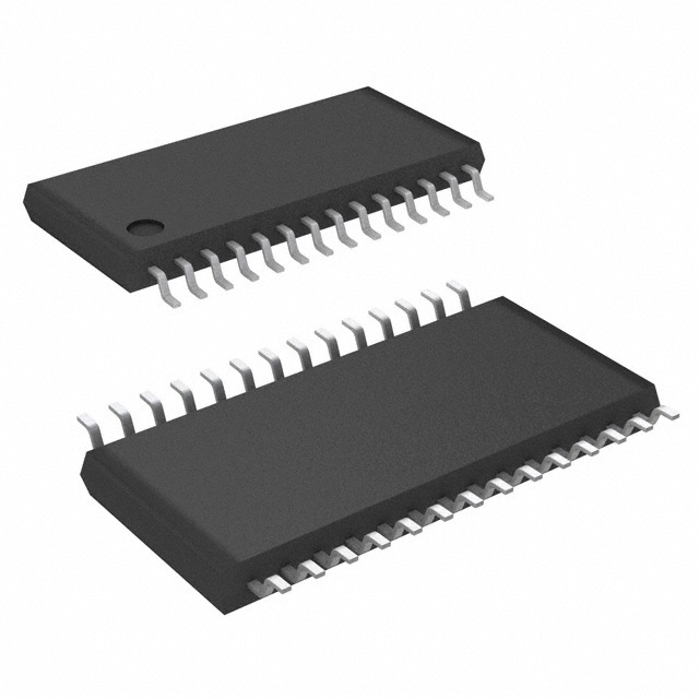
Package: 28-pin TSSOP, Pin Pitch: 0,65 mm
The DIR9001 supports many output system clock and
output data formats and can be used flexibly in many
application systems. As the all functions which the
DIR9001 provides can be controlled directly through
control pins, it can be used easily in an application
system that does not have a microcontroller. Also, as
dedicated pins are provided for the channel-status bit
and user-data bit, processing of their information can
be easily accomplished by connecting with a
microcontroller, DSP, or others.
The DIR9001 does not require an external clock
source or resonator for decode operation if the
internal actual-sampling-frequency calculator is not
used. Therefore, it is possible to reduce the cost of a
system.
The operating temperature range of the DIR9001 is
specified as –40°C to 85°C, which makes it suitable
for automotive applications.
Device Information
PART NUMBER
DIR9001
PACKAGE
Block Diagram
XTI
2 Applications
AV/DVD Receiver, AV Amplifier
Car or Mobile Audio System
Digital Television
Musical Instruments
Recording Systems
High-End Audio/Sound Card for PC
Replacement of DIR1703
Other Applications Requiring S/PDIF Receiver
4.40 mm × 9.70 mm
(1) For all available packages, see the orderable addendum at
the end of the data sheet.
FILT
•
•
•
•
•
•
•
•
BODY SIZE (NOM)
TSSOP (28)
XTO
OSC
Sampling
Frequency
Calculator
FSOUT0
FSOUT1
Clock and Data Recovery
SCKO
RXIN
Preamble
Detector
Charge
Pump
VCO
Divider
PLL
BCKO
Divider
Clock
Decoder
LRCKO
Biphase
Data Decoder
PSCK0
Function
Control
Decoder
CKSEL
Audio Data
MUTE Control
DGND
PSCK1
Power Supply
RESET
VDD
DGND
VCC
DOUT
UOUT
Channel Status
and
User Data
Output
RSV
RST
ERROR
CLKST
Serial
Audio Data
Formatter
FMT0
FMT1
ERROR
Detector
COUT
BFRAME
AUDIO
EMPH
AGND
1
An IMPORTANT NOTICE at the end of this data sheet addresses availability, warranty, changes, use in safety-critical applications,
intellectual property matters and other important disclaimers. PRODUCTION DATA.
�DIR9001
SLES198A – DECEMBER 2006 – REVISED MAY 2015
www.ti.com
Table of Contents
1
2
3
4
5
Features ..................................................................
Applications ...........................................................
Description .............................................................
Revision History.....................................................
Device Comparison Table.....................................
1
1
1
2
3
5.1 Differences From DIR1703 ....................................... 3
6
7
Pin Configuration and Functions ......................... 4
Specifications......................................................... 6
7.1
7.2
7.3
7.4
7.5
7.6
7.7
7.8
8
Absolute Maximum Ratings ...................................... 6
ESD Ratings.............................................................. 6
Recommended Operating Conditions....................... 6
Thermal Information .................................................. 7
Electrical Characteristics........................................... 7
Timing Requirements ................................................ 8
Switching Characteristics .......................................... 9
Typical Characteristics ............................................ 10
Detailed Description ............................................ 11
8.1 Overview ................................................................. 11
8.2
8.3
8.4
8.5
9
Functional Block Diagram .......................................
Feature Description.................................................
Device Functional Modes........................................
Programming...........................................................
11
12
20
23
Application and Information ............................... 26
9.1 Application Information............................................ 26
9.2 Typical Application .................................................. 27
10 Power Supply Recommendations ..................... 29
11 Layout................................................................... 29
11.1 Layout Guidelines ................................................. 29
11.2 Layout Example .................................................... 30
12 Device and Document Support.......................... 31
12.1
12.2
12.3
12.4
Community Resources..........................................
Trademarks ...........................................................
Electrostatic Discharge Caution ............................
Glossary ................................................................
31
31
31
31
13 Mechanical, Packaging, and Orderable
Information ........................................................... 31
4 Revision History
Changes from Original (Dec 2006) to Revision A
•
2
Page
Added Pin Configuration and Functions section, ESD Ratings table, Feature Description section, Device Functional
Modes, Application and Implementation section, Power Supply Recommendations section, Layout section, Device
and Documentation Support section, and Mechanical, Packaging, and Orderable Information section .............................. 1
Submit Documentation Feedback
Copyright © 2006–2015, Texas Instruments Incorporated
Product Folder Links: DIR9001
�DIR9001
www.ti.com
SLES198A – DECEMBER 2006 – REVISED MAY 2015
5 Device Comparison Table
5.1 Differences From DIR1703
The DIR9001 has many improved functions compared to the DIR1703.
The DIR9001 functions are similar to those of the DIR1703.
The DIR9001 pin assignment is equivalent to that of the DIR1703.
The DIR9001 biphase input signal decoding function is almost equivalent to that of the DIR1703.
The differences between the DIR9001 and DIR1703 are shown in Table 1.
Table 1. Main Differences Between DIR1703 and DIR9001
DIFFERENCE
DIR1703
DIR9001
Operational supply-voltage range
3 V to 3.6 V
2.7 V to 3.6 V
Operation temperature range
–25°C to 85°C
–40°C to 85°C
Package
SSOP-28P, pin pitch: 0.65 mm
TSSOP-28P, pin pitch: 0.65 mm
Clock recovery architecture
SpAct™ feature
Conventional PLL
IEC60958-3 jitter tolerance
Not compliant
Compliant
IEC60958 sampling frequency accuracy
Level II (±1000 ppm)
Level III (±12.5%)
Acceptable sampling frequency
32/44.1/48/88.2/96 kHz, ±1500 ppm
28 kHz to 108 kHz continuous
Biphase input signal level
CMOS level
5-V tolerant TTL level
Connection of loop filter
Between FILT pin and VCC
Between FILT pin and AGND
XTI source clock frequency
One of the following clock sources or
resonators must be connected to the XTI pin:
4.069/5.6448/6.144/ 8.192/11.2896/12.288/
16.384/16.9344/18.432/ 22.5792/24.576-MHz
Optional 24.576-MHz (24.576-MHz clock is
only required to use the internal actualsampling-frequency calculator or use the
DIR9001 as a 24.576-MHz clock generator.)
BFRAME H period
32/fS
8/fS
Channel status and user data
Synchronous with LRCK transition
17-BCK delay from LRCK transition
Latest tracked frequency hold
Available
Not available
PLL mode clock at error
Latest tracked frequency
VCO free-running frequency
Clock transition signal out
CKTRNS pin, active H
CLKST pin, active-high
Oscillation amplifier
External feedback resistor (typ. 1 MΩ)
Internal feedback resistor
The differences between the DIR1703 and DIR9001 I/O pins are shown in Table 2.
Table 2. The Differences Between DIR1703 and DIR9001 in All I/O Pin
PIN NO.
DIR1703
DIR9001
DIFFERENCES
1
ADFLG
AUDIO
Pin name only
Channel-status data information of non-audio sample word, active-low
DESCRIPTIONS OF DIR9001
2
BRATE0
FSOUT0
Pin name only
Actual-sampling-frequency calculated result output 0
3
BRATE1
FSOUT1
Pin name only
Actual-sampling-frequency calculated result output 1
4
SCKO
SCKO
Same function
System clock output
5
VDD
VDD
Same function
Digital power supply, 3.3-V
6
DGND
DGND
Same function
Digital ground
7
XTO
XTO
Same function
Oscillation amplifier output
8
XTI
XTI
Same function
Oscillation amplifier input, or external XTI source clock input
9
CKTRNS
CLKST
CLKST is active-high
10
LRCKO
LRCKO
Same function
Audio data latch enable output
11
BCKO
BCKO
Same function
Audio data bit clock output
12
DOUT
DOUT
Same function
16 bit–24 bit decoded serial digital audio data output
13
SCF0
PSCK0
Pin name only
SCKO output frequency selection 0
14
SCF1
PSCK1
Pin name only
SCKO output frequency selection 1
15
CSBIT
COUT
Pin name only
Channel-status data serial output synchronized with LRCKO
Clock change/transition signal output
Submit Documentation Feedback
Copyright © 2006–2015, Texas Instruments Incorporated
Product Folder Links: DIR9001
3
�DIR9001
SLES198A – DECEMBER 2006 – REVISED MAY 2015
www.ti.com
Table 2. The Differences Between DIR1703 and DIR9001 in All I/O Pin (continued)
PIN NO.
DIR1703
DIR9001
DIFFERENCES
16
URBIT
UOUT
Pin name only
User data serial output synchronized with LRCKO
DESCRIPTIONS OF DIR9001
17
EMFLG
EMPH
Pin name only
Channel-status data Information of pre-emphasis (50 μs/15 μs)
18
BFRAME
BFRAME
Same function
Indication of top block of biphase input signal
19
BRSEL
RSV
Reserved
20
DIN
RXIN
Pin name only
Biphase digital data input
21
RST
RST
Same function
Reset control input, active-low
22
FILT
FILT
Same function
External filter connection terminal. Recommended filter must be connected.
23
AGND
AGND
Same function
Analog ground
24
VCC
VCC
Same function
Analog power supply, 3.3-V
25
FMT0
FMT0
Same function
Decoded serial digital audio data output format selection 0
26
FMT1
FMT1
Same function
Decoded serial digital audio data output format selection 1
27
UNLOCK
ERROR
Pin name only
Indication of internal PLL or data parity error
28
CKSEL
CKSEL
Same function
Selection of system clock source, Low: PLL (VCO) clock, High: XTI clock
Reserved, must be connected to DGND
6 Pin Configuration and Functions
DIR9001
(TOP VIEW)
4
CKSEL
28
ERROR
27
1
AUDIO
2
FSOUT0
3
FSOUT1
FMT1 26
4
SCKO
FMT0
5
VDD
6
DGND
7
25
VCC 24
AGND
23
XTO
FILT
22
8
XTI
RST
21
9
CLKST
RXIN
20
10
LRCKO
RSV
19
11
BCKO
BFRAME
18
12
DOUT
EMPH
17
13
PSCK0
UOUT
16
14
PSCK1
COUT
15
Submit Documentation Feedback
Copyright © 2006–2015, Texas Instruments Incorporated
Product Folder Links: DIR9001
�DIR9001
www.ti.com
SLES198A – DECEMBER 2006 – REVISED MAY 2015
Pin Functions
PIN
I/O
PULL
UP/DOWN
REMARKS
DESCRIPTION
NAME
NO.
AGND
23
–
AUDIO
1
OUT
CMOS
Channel-status data information of non-audio sample word, active-low
BCKO
11
OUT
CMOS
Audio data bit clock output
BFRAME
18
OUT
CMOS
Indication of top block of biphase input signal
CKSEL
28
IN
CLKST
9
OUT
CMOS
Clock change/transition signal output
COUT
15
OUT
CMOS
Channel-status data serial output synchronized with LRCKO
DGND
6
–
DOUT
12
OUT
CMOS
16-bit/24-bit decoded serial digital audio data output
EMPH
17
OUT
CMOS
Channel-status data information of pre-emphasis (50 μs/15 μs)
ERROR
27
OUT
CMOS
Indication of internal PLL or data parity error
FILT
22
–
FMT0
25
IN
Pulldown
5-V tolerant TTL
Decoded serial digital audio data output format selection 0 (1)
FMT1
26
IN
Pulldown
5-V tolerant TTL
Decoded serial digital audio data output format selection 1 (1)
FSOUT0
2
OUT
CMOS
Actual sampling frequency calculated result output 0
FSOUT1
3
OUT
CMOS
Actual sampling frequency calculated result output 1
LRCKO
10
OUT
CMOS
Audio data latch enable output
PSCK0
13
IN
Pulldown
5-V tolerant TTL
PLL source SCKO output frequency selection 0(1)
PSCK1
14
IN
Pulldown
5-V tolerant TTL
PLL source SCKO output frequency selection 1 (1)
RST
21
IN
Pullup
5-V tolerant TTL
Reset control input, active-low
RSV
19
IN
Pulldown
RXIN
20
IN
5-V tolerant TTL
SCKO
4
OUT
CMOS
System clock output
UOUT
16
OUT
CMOS
User data serial output synchronized with LRCKO
VCC
24
–
Analog power supply, 3.3-V
VDD
5
–
Digital power supply, 3.3-V
XTI
8
IN
CMOS
Schmitt-trigger
XTO
7
OUT
CMOS
(1)
(2)
(3)
Analog ground
Pulldown
5-V tolerant TTL
Selection of system clock source, Low: PLL (VCO) clock, High: XTI clock (1)
Digital ground
External filter connection terminal; must connect recommended filter.
(2)
Reserved, must be connected to DGND(1)
Biphase digital data input (3)
Oscillation amplifier input, or external XTI source clock input
Oscillation amplifier output
TTL Schmitt-trigger input with internal pulldown (51 kΩ typical), 5-V tolerant
TTL Schmitt-trigger input with internal pullup (51 kΩ typical), 5-V tolerant
TTL Schmitt-trigger input, 5-V tolerant.
Submit Documentation Feedback
Copyright © 2006–2015, Texas Instruments Incorporated
Product Folder Links: DIR9001
5
�DIR9001
SLES198A – DECEMBER 2006 – REVISED MAY 2015
www.ti.com
7 Specifications
7.1 Absolute Maximum Ratings
over operating free-air temperature range (unless otherwise noted)
(1)
MIN
MAX
UNIT
Supply voltage
–0.3
4
V
VCC to VDD
Supply voltage differences
–0.1
0.1
V
AGND to
DGND
Ground voltage differences
–0.1
0.1
V
VCC
VDD
Tstg
(1)
Digital input
voltage
Digital input
–0.3
6.5
Digital output
–0.3
(VDD + 0.3) < 4
Analog input
voltage
XTI, XTO
–0.3
(VCC + 0.3) < 4
FILT
–0.3
(VCC + 0.3) < 4
V
V
Input current (any pins except supplies)
–10
10
mA
Ambient temperature under bias
–40
125
°C
Junction temperature
150
°C
Lead temperature (soldering)
260
°C
Package temperature (reflow, peak)
260
°C
150
°C
Storage temperature
–55
Stresses beyond those listed under Absolute Maximum Ratings may cause permanent damage to the device. These are stress ratings
only and functional operation of the device at these or any other conditions beyond those indicated under recommended operating
conditions is not implied. Exposure to absolute-maximum-rated conditions for extended periods may affect device reliability.
7.2 ESD Ratings
VALUE
Human body model (HBM), per ANSI/ESDA/JEDEC JS-001
V(ESD)
(1)
(2)
Electrostatic discharge
(1)
UNIT
±500
Charged-device model (CDM), per JEDEC specification JESD22C101 (2)
V
±250
JEDEC document JEP155 states that 500-V HBM allows safe manufacturing with a standard ESD control process.
JEDEC document JEP157 states that 250-V CDM allows safe manufacturing with a standard ESD control process.
7.3 Recommended Operating Conditions
over operating free-air temperature range (unless otherwise noted)
MIN
NOM
MAX
UNIT
VCC
Analog supply voltage
2.7
3.3
3.6
VDC
VDD
Digital supply voltage
2.7
3.3
3.6
VDC
Digital input clock frequency
TA
6
XTI is connected to clock source
XTI is connected to DGND
24.576
MHz
Not required
MHz
Digital output load capacitance, except SCKO
20
pF
Digital output load capacitance (SCKO)
10
pF
85
°C
Operating free-air temperature
–40
Submit Documentation Feedback
Copyright © 2006–2015, Texas Instruments Incorporated
Product Folder Links: DIR9001
�DIR9001
www.ti.com
SLES198A – DECEMBER 2006 – REVISED MAY 2015
7.4 Thermal Information
DR9001
THERMAL METRIC (1)
TSSOP (PW)
UNIT
28 PINS
RθJA
Junction-to-ambient thermal resistance
81.9
°C/W
RθJC(top)
Junction-to-case (top) thermal resistance
22.5
°C/W
RθJB
Junction-to-board thermal resistance
40
°C/W
ψJT
Junction-to-top characterization parameter
0.7
°C/W
ψJB
Junction-to-board characterization parameter
39.4
°C/W
(1)
For more information about traditional and new thermal metrics, see the IC Package Thermal Metrics application report, SPRA953.
7.5 Electrical Characteristics
All specifications at TA = 25°C, VDD = VCC = 3.3 V (unless otherwise noted)
PARAMETER
TEST CONDITIONS
MIN
TYP
MAX
UNIT
DIGITAL INPUT/OUTPUT CHARACTERISTICS
VIH
VIL
VIH
VIL
VOH
VOL
IIH
IIL
IIH
IIL
IIH
IIL
0.7 VDD
Input logic level (1)
2
Input logic level (2)
Output logic level (3)
Input leakage current (4)
Input leakage current (5)
Input leakage current (6)
VDD
VDC
0.3 VDD
5.5
VDC
0.8
IO = 4 mA
0.85 VDD
IO = –4 mA
VDC
0.15 VDD
VIN = VDD
65
100
VIN = 0 V
–10
10
VIN = VDD
–10
10
VIN = 0 V
–100
VIN = VDD
–10
10
VIN = 0 V
–10
10
μA
μA
–65
μA
BIPHASE SIGNAL INPUT AND PLL
Jitter tolerance — (IEC60958-3)
IEC60958-3 (2003-01)
Compliant
RECOVERED CLOCK AND DATA
Serial audio data width
SCKO jitter
16
fS = 48 kHz, SCKO = 256 fS, measured
periodic
50
24
Bit
100
ps rms
100
ppm
XTI SOURCE CLOCK
Frequency accuracy
XTI is connected to clock source
–100
POWER SUPPLY AND SUPPLY CURRENT
VCC
VDD
ICC
2.7
3.3
3.6
2.7
3.3
3.6
fS = 96 kHz, PLL locked, XTI connected
to DGND
6
8.3
mA
fS = 96 kHz, PLL locked, XTI connected
to 24.576-MHz resonator
6
8.3
mA
Operation voltage range
Supply current (7)
RXIN = H or L, XTI = L, RST = L
(1)
(2)
(3)
(4)
(5)
(6)
(7)
130
VDC
μA
CMOS compatible input: XTI (not 5-V tolerant)
5-V tolerant TTL inputs: RXIN, FMT0, FMT1, PSCK0, PSCK1, CKSEL, RST, RSV
CMOS outputs: XTO, SCKO, BCKO, LRCKO, DOUT, UOUT, COUT, BFRAME, ERROR, CLKST, AUDIO, EMPH, FSOUT0, FSOUT1
Internal pulldowns: FMT0, FMT1, PSCK0, PSCK1, CKSEL, RSV
Internal pullup: RST
No internal pullup and pulldown: RXIN, XTI
No load connected to SCKO, BCKO, LRCKO, DOUT, COUT, VOUT, BFRAME, FSOUT0, FSOUT1, CLKST, ERROR, EMPH, AUDIO
Submit Documentation Feedback
Copyright © 2006–2015, Texas Instruments Incorporated
Product Folder Links: DIR9001
7
�DIR9001
SLES198A – DECEMBER 2006 – REVISED MAY 2015
www.ti.com
Electrical Characteristics (continued)
All specifications at TA = 25°C, VDD = VCC = 3.3 V (unless otherwise noted)
PARAMETER
Supply current (7)
IDD
Power dissipation (7)
PD
TEST CONDITIONS
MIN
TYP
MAX
UNIT
fS = 96 kHz, PLL locked, XTI connected
to DGND
6
8.3
mA
fS = 96 kHz, PLL locked, XTI connected
to 24.576-MHz resonator
9
12.4
mA
μA
RXIN = H or L, XTI = L, RST = L
72
fS = 96 kHz, PLL locked, XTI connected
to DGND
40
55
mW
fS = 96 kHz, PLL locked, XTI connected
to 24.576-MHz resonator
50
68
mW
RXIN = H or L, XTI = L, RST = L
0.67
mW
TEMPERATURE RANGE
TA
Operation temperature range
θJA
Thermal resistance
–40
85
28-pin T-SSOP
105
°C
°C/W
7.6 Timing Requirements
All specifications at TA = 25°C, VDD = VCC = 3.3 V (unless otherwise noted)
MIN
NOM
MAX
UNIT
108
kHz
BIPHASE SIGNAL INPUT AND PLL
Input sampling frequency range
28
XTI SOURCE CLOCK
XTI is connected to clock source
XTI source clock frequency
XTI is connected to DGND
XTI input-clock duty cycle
24.576
MHz
Not required
XTI is connected to clock source
45%
55%
4
20
CLKST
tCLKST
CLKST pulse duration, high
μs
LATENCY
tLATE
LRCKO/DOUT latency
See Figure 14
3/fS
s
DATA OUTPUT (1)
tSCY
System clock pulse cycle time
tSCBC
Delay time of SCK rising edge to BCK rising
edge
tCKLR
Delay time of BCKO falling edge to LRCKO valid
tBCY
BCKO pulse cycle time
tBCH
BCKO pulse duration, HIGH
60
tBCL
BCKO pulse duration, LOW
60
tBCDO
Delay time of BCKO falling edge to DOUT valid
–5
tr
tf
(1)
8
18
4
–5
See Figure 16
ns
8
15
ns
0.5
0.5
ns
1/64fS
s
ns
ns
1
5
ns
Rising time of all signals
10
ns
Falling time of all signals
10
ns
Load capacitance of the LRCKO, BCKO, and DOUT pins is 20 pF. DOUT, LRCKO, and BCKO are synchronized with SCKO.
Submit Documentation Feedback
Copyright © 2006–2015, Texas Instruments Incorporated
Product Folder Links: DIR9001
�DIR9001
www.ti.com
SLES198A – DECEMBER 2006 – REVISED MAY 2015
7.7 Switching Characteristics
All specifications at TA = 25°C, VDD = VCC = 3.3 V (unless otherwise noted)
PARAMETER
TEST CONDITIONS
MIN
TYP
MAX
UNIT
100
ms
BIPHASE SIGNAL INPUT AND PLL
PLL lock-up time
From biphase signal detection to
error-out release (ERROR = L)
RECOVERED CLOCK AND DATA
SCKO frequency
128 fS
3.584
13.824
256 fS
7.168
27.648
384 fS
10.752
41.472
MHz
512 fS
14.336
55.296
BCKO frequency
64 fS
1.792
6.912
MHz
LRCKO frequency
fS
28
108
kHz
45%
55%
SCKO duty cycle
Submit Documentation Feedback
Copyright © 2006–2015, Texas Instruments Incorporated
Product Folder Links: DIR9001
9
�DIR9001
SLES198A – DECEMBER 2006 – REVISED MAY 2015
www.ti.com
7.8 Typical Characteristics
Oscillation amplifier operating with crystal; 1-kHz, 0-dB, sine-wave data; no load
20
20
VCC = VDD = 3.3 V
SCKO = 256 fS
18
ICC + IDD − Supply Current − mA
18
ICC + IDD − Supply Current − mA
TA = 25°C
SCKO = 256 fS
16
14
85°C
12
–40°C
50°C
25°C
–25°C
10
0°C
16
14
3.3 V
3.6 V
12
10
2.7 V
3V
8
8
6
6
30
40
50
60
70
80
90
30
100
fS − Sampling Frequency − kHz
40
50
60
70
80
fS − Sampling Frequency − kHz
G001
Figure 1. Supply Current vs Locked Sampling Frequency
90
100
G002
Figure 2. Supply Current vs Locked Sampling Frequency
200
VCC = VDD = 3.3 V
TA = 25°C
180
Periodic Jitter − ps rms
160
128 fS
140
120
256 fS
100
80
384 fS
512 fS
60
40
20
30
40
50
60
70
80
fS − Sampling Frequency − kHz
90
100
G003
Figure 3. Scko Jitter vs Locked Sampling Frequency
10
Submit Documentation Feedback
Copyright © 2006–2015, Texas Instruments Incorporated
Product Folder Links: DIR9001
�DIR9001
www.ti.com
SLES198A – DECEMBER 2006 – REVISED MAY 2015
8 Detailed Description
8.1 Overview
The DIR9001 is a digital audio interface receiver that can receive a 28-kHz to 108-kHz sampling frequency, 24bit-data-word, biphase-encoded signal and output a serial audio signal. The DIR9001 complies with the jitter
specification IEC60958-3, JEITA CPR1205 (Revised version of EIAJ CP-1201), AES3, EBUtech3250, and it can
be used in various applications that require a digital audio interface.
The DIR9001 supports MSB-first PCM data output in 24-bit I2S, 24-bit left justified, 24-bit right justified, or 16-bit
right justified form. Sampling rates of 32 kHz, 44.1 kHz, 48 kHz, 88.2 kHz, and 96 kHz are supported on the
serial audio data output when in PLL mode. All functions which the DIR9001 provides can be controlled directly
through control pins. This means that they can be pulled high or low for full operation of the DIR9001 without a
microcontroller. A microcontroller can also be used to drive the function pins to provide an adaptable system.
Also, as dedicated pins are provided for the channel-status bit and user-data bit, processing of their information
can be easily accomplished by connecting with a microcontroller, DSP, and so on.
The DIR9001 can derive a system clock by recovering the source’s clock from the biphase input signal.
Therefore, the DIR9001 does not require an external clock source or resonator for decode operation if the
internal actual-sampling-frequency calculator is not used which in turn can reduce the system cost. The serial
audio data output can also be driven by an external source such as a crystal or ceramic resonator.
The operating temperature range of the DIR9001 is specified as –40°C to 85°C, which makes it suitable for
automotive applications.
8.2 Functional Block Diagram
FILT
XTI
XTO
OSC
Sampling
Frequency
Calculator
FSOUT0
FSOUT1
Clock and Data Recovery
SCKO
RXIN
Charge
Pump
Preamble
Detector
VCO
Divider
PLL
BCKO
Divider
Clock
Decoder
LRCKO
Biphase
Data Decoder
PSCK0
Function
Control
Decoder
CKSEL
Audio Data
MUTE Control
DGND
PSCK1
Power Supply
RESET
VDD
DGND
VCC
DOUT
UOUT
Channel Status
and
User Data
Output
RSV
RST
ERROR
CLKST
Serial
Audio Data
Formatter
FMT0
FMT1
ERROR
Detector
COUT
BFRAME
AUDIO
EMPH
AGND
Submit Documentation Feedback
Copyright © 2006–2015, Texas Instruments Incorporated
Product Folder Links: DIR9001
11
�DIR9001
SLES198A – DECEMBER 2006 – REVISED MAY 2015
www.ti.com
8.3 Feature Description
8.3.1 Acceptable Biphase Input Signal and Biphase Input Pin (RXIN)
The DIR9001 can decode the biphase signal format which is specified in one of the following standards.
Generally, these following standards may be called Sony/Philips digital interface format (S/PDIF) or AES/EBU.
• IEC60958 (revised edition of former IEC958)
• JEITA CPR-1205 (revised edition of former EIAJ CP-1201, CP-340)
• AES3
• EBU tech3250
The sampling frequency range and data word length which DIR9001 can decode is as follows:
• Sampling frequency range is 28 kHz to 108 kHz.
• Maximum audio sample word length is 24-bit.
Note of others about the biphase input signal.
• The capture ratio of the built-in PLL complies with level III of sampling frequency accuracy (±12.5%), which is
specified in IEC60958-3.
• The jitter tolerance of the DIR9001 complies with IEC60958-3.
• The PLL may also lock in outside of the specified sampling-frequency range, but extended range is not
assured.
Notice about the signal level and transmission line of the biphase input signal.
• The signal level and the transmission line (optical, differential, single-ended) are different in each standard.
• The biphase input signal is connected to the RXIN pin of the DIR9001.
• The RXIN pin has a 5-V tolerant TTL-level input.
• An optical receiver module (optical to electric converter) such as TOSLINK, which is generally used in
consumer applications, is connected directly to the RXIN pin without added external components.
• The output waveform of the optical receiver module varies depending on the characteristics of each product
type, so a dumping resistor or buffer amplifier might be required between the optical receiver module output
and the DIR9001 input. Careful handling is required if the optical receiver module and the DIR9001 are
separated by a long distance.
• The DIR9001 needs an external amplifier if it is connected to a coaxial transmission line.
• The DIR9001 needs an external differential to single-ended converter, attenuator, etc., for general consumer
applications if non-optical transmission line is used.
8.3.2 System Reset
The DIR9001 reset function is controlled by and external reset pin, RST.
The reset operation must be performed during the power-up sequence as shown in Figure 4. Specifically, the
DIR9001 requires reset operation with a 100-ns period after the supply voltage rises above 2.7 V.
2.7 V
VDD
RST
DIR9001
Status
Unknown
Operation
Reset
Min. 100 ns
Figure 4. Required System Reset Timing
12
Submit Documentation Feedback
Copyright © 2006–2015, Texas Instruments Incorporated
Product Folder Links: DIR9001
�DIR9001
www.ti.com
SLES198A – DECEMBER 2006 – REVISED MAY 2015
Feature Description (continued)
The state of each output pins during reset is shown in Table 3.
Table 3. Output-Pin States During Reset Period
CLASSIFICATION
PIN NAME
WHILE RST = L
BCKO
L
Clock
LRCKO
L
SCKO
L
Data
Flag and status
Oscillation amplifier
DOUT
L
AUDIO
L
BFRAME
L
CLKST
L
COUT
L
EMPH
L
ERROR
H
FSOUT0
L
FSOUT1
L
UOUT
L
XTO
Output
8.3.3 Clock Description
8.3.3.1 System Clock Source
DIR9001 has the following two clock sources for the system clock.
• PLL source (128 fS, 256 fS, 384 fS, 512 fS are available, recovered by built-in PLL)
• XTI source (One 24.576-MHz resonator or external clock source is required.)
Two clock sources are used for the following purpose.
• PLL source: Recovered system clock from the biphase input signal
• XTI source: Clock source for peripheral devices (for example, A/D converter, microcontroller, etc.)
Measurement reference clock for the internal actual-sampling-frequency calculator
Description of PLL clock source
• The PLL clock source is the output clock of built-in PLL (including VCO).
• The PLL clock source frequency is selectable from 128 fS, 256 fS, 384 fS, 512 fS by PSCK[1:0].
• When the PLL is in the locked condition, the PLL clock source is the clock recovered from the biphase input
signal.
• When PLL is in the unlocked condition, the PLL clock source is the built-in free-running clock of the VCO.
• The frequency of the PLL clock source in the unlocked condition is not constant.
(The VCO free-running frequency is dependent on supply voltage, temperature, and variations in the die’s
wafer.)
Description of XTI clock source
• The XTI clock source is not used to recover the clock and decode data from the biphase input signal.
• Therefore, if the DIR9001 is used only for recovering the clock and decoding data from the biphase input
signal, an XTI clock source is not required. In this case, the XTI pin must be connected to the DGND pin.
(The DIR9001 does not have a selection pin for using an XTI clock source or not using one.)
The selection method of clock source
• The output clock is selected from two clock sources by the level of the CKSEL pin.
• The selection of the system clock source depends only on the input level of CKSEL pin.
• CKSEL = L setting is required for recovering the clock and decoding data from biphase input.
• CKSEL = H setting is required for XTI clock source output.
• The continuity of clock during the clock source transition between the XTI source and the PLL source is not
Submit Documentation Feedback
Copyright © 2006–2015, Texas Instruments Incorporated
Product Folder Links: DIR9001
13
�DIR9001
SLES198A – DECEMBER 2006 – REVISED MAY 2015
www.ti.com
assured.
Method of automatic clock source selection (CLOCK SOURCE MODE: AUTO)
• This method enables selection of the clock source automatically, using the DIR9001 ERROR status. The PLL
source clock is output when ERROR = L; the XTI source is output when ERROR = H.
• To enable automatic clock source selection, the CKSEL pin must be connected to the ERROR pin.
• If XTI clock source is needed during the ERROR period, this method is recommended.
• Because the clock source during ERROR status is XTI, if an XTI clock source is not provided to the XTI pin,
then SCKO, BCKO, and LRCKO are not output during the ERROR period.
The relationship between the clock/data source and the combination of CKSEL pin and PLL status inputs is
shown in Table 12.
The clock tree system is shown in Figure 5.
[PSCK1]
[PSCK0]
RXIN
VCO
1/N
CKSEL (I)
Built-in PLL
Clock Recovery
PLL Clock Source
1/N
SCKO (O)
1/N
BCKO (O)
XTI (I)
LRCKO (O)
1/4
XTO (O)
Oscillation Amplifier
1/64
Clock Source
Selector
XTI Clock Source
Figure 5. Clock Tree Diagram
8.3.4 PLL Clock Source (Built-In PLL and VCO) Description
The DIR9001 has on-chip PLL (including VCO) for recovering the clock from the biphase input signal.
The clock that is output from the built-in VCO is defined as the PLL clock source.
In the locked state, the built-in PLL generates a system clock that synchronizes with the biphase input signal.
In the unlocked state, the built-in PLL (VCO) generates a free-running clock. (The frequency is not constant.)
The PLL can support a system clock of 128 fS, 256 fS, 384 fS, or 512 fS, where fS is the sampling frequency of the
biphase input signal.
The system clock frequency of the PLL is selected by PSCK[1:0].
The DIR9001 can decode a biphase input signal through its sampling-frequency range of 28 kHz to 108 kHz,
independent of the setting of PSCK[1:0].
Therefore, the DIR9001 can decode a biphase input signal with a sampling frequency from 28 kHz to 108 kHz at
all settings of PSCK[1:0]
The relationship between the PSCK[1:0] selection and the output clock (SCKO, BCKO, LRCKO) from the PLL
source is shown in Table 4.
14
Submit Documentation Feedback
Copyright © 2006–2015, Texas Instruments Incorporated
Product Folder Links: DIR9001
�DIR9001
www.ti.com
SLES198A – DECEMBER 2006 – REVISED MAY 2015
Table 4. SCKO, BCKO, and LRCKO Frequencies Set by PSCK[1:0]
PSCK[1:0] SETTING
PSCK1
OUTPUT CLOCK FROM PLL SOURCE
PSCK0
SCKO
BCKO
LRCKO
L
L
128 fS
64 fS
fS
L
H
256 fS
64 fS
fS
H
L
384 fS
64 fS
fS
H
H
512 fS
64 fS
fS
In PLL mode (CKSEL = L), output clocks (SCKO, BCKO, LRCKO) are generated from the PLL source clock.
The relationship between frequencies of LRCKO, BCKO, and SCKO at different sampling frequencies fS of the
biphase input signal are shown in Table 5.
Table 5. Output Clock Frequency in PLL Locked State (CKSEL = L)
LRCKO
BCKO
fS
64 fS
128 fS
SCKO (DEPENDING ON PSCK[1:0] SETTING)
256 fS
384 fS
512 fS
32 kHz
2.048 MHz
4.096 MHz
8.192 MHz
12.288 MHz
16.384 MHz
44.1 kHz
2.8224 MHz
5.6448 MHz
11.2896 MHz
16.9344 MHz
22.5792 MHz
48 kHz
3.072 MHz
6.144 MHz
12.288 MHz
18.432 MHz
24.576 MHz
88.2 kHz
5.6448 MHz
11.2896 MHz
22.5792 MHz
33.8688 MHz
45.1584 MHz
96 kHz
6.144 MHz
12.288 MHz
24.576 MHz
36.864 MHz
49.152 MHz
8.3.5 Required PLL Loop Filter Description
The DIR9001 incorporates a PLL for generating a clock synchronized with the biphase input signal.
The built-in PLL requires an external loop filter, which is specified as follows.
Operation and performance is assured for recommended filter components R1, C1, and C2.
Notes about Loop Filter Components and Layout
• The resistor and capacitors which comprise the filter should be located and routed as close as possible to the
DIR9001.
• A carbon film resistor or metal film resistor, with tolerance less than 5%, is recommended.
• Film capacitors, with tolerance is less than 5%, is recommended.
• If ceramic capacitors are used for C1 and C2, parts with a low voltage coefficient and low temperature
coefficient, such as CH or C0G, are recommended.
• The external loop filter must be placed on FILT pins.
• The GND node of the external loop filter must be directly connected with the AGND pin of the DIR9001; it
must be not combined with other signals.
The configuration of external loop filter and the connection with the DIR9001 is shown in Figure 6.
DIR9001
PLL Section
Charge
Pump
VCO
AGND
FILT
DGND
C2
R1
C1
Figure 6. Loop Filter Connection
Submit Documentation Feedback
Copyright © 2006–2015, Texas Instruments Incorporated
Product Folder Links: DIR9001
15
�DIR9001
SLES198A – DECEMBER 2006 – REVISED MAY 2015
www.ti.com
The recommended values of loop filter components is shown in Table 6.
Table 6. Recommended Value of Loop Filter Components
REF. NO.
RECOMMENDED VALUE
PARTS TYPE
TOLERANCE
R1
680 Ω
Metal film or carbon
≤5%
C1
0.068 μF
Film or ceramic (CH or C0G)
≤5%
C2
0.0047 μF
Film or ceramic (CH or C0G)
≤5%
8.3.6 XTI Clock Source and Oscillation Amplifier Description
This clock, driven by the built-in oscillation amplifier or input into the XTI pin from an external clock, is defined as
the XTI source. A 24.576-MHz fundamental resonator or external 24.576-MHz clock is used as the XTI source.
The DIR9001 requires an XTI source for following purposes:
• The measurement reference clock of actual-sampling-frequency calculator
• The clock source for the XTI source mode (CKSEL = H setting)
(That is, the DIR9001 does not require an XTI source if it is only decoding the biphase input signal.)
The XTI clock source is supplied in one of the following two ways; the details are described in Figure 7.
• Setting up an oscillation circuit by connecting a resonator with the built-in amplifier
• Applying a clock from an external oscillator circuit or oscillator module
To
•
•
•
•
•
set up an oscillation circuit by connecting a resonator with the built-in amplifier:
Connect a 24.576-MHz resonator between the XTI pin and XTO pin.
The resonator should be a fundamental-mode type.
A crystal resonator or ceramic resonator can be used.
The load capacitor CL1, CL2, and the current-limiting resistor Rd depend on the characteristics of the
resonator.
No external feedback resistor between the XTI pin and XTO pin is required, as an appropriate resistor is
incorporated in the device.
No load other than the resonator is allowed on the XTO pin.
To
•
•
•
connect an external oscillator circuit or oscillator module:
Provide a 24.576-MHz clock on the XTI pin
Note that the XTI pin is not 5-V tolerant; it is simple CMOS input.
The XTO pin must be open.
•
Crystal
OSC
Circuit
Resonator
XTI
CL1
Rd
24.576 MHz
Internal Clock
XTI
External
Clock
Must Be
Open
XTO
CL2
Crystal
OSC
Circuit
24.576 MHz
Internal Clock
XTO
DIR9001
DIR9001
Resonator Connection
External Clock Input Connection
Figure 7. XTI and XTO Connection Diagram
Description of oscillation amplifier operation:
• The built-in oscillation amplifier is always working.
• If the XTI source clock is not used, then the XTI pin must be connected to DGND.
• For reducing power dissipation, it is recommended to not use the XTI source clock.
In XTI mode (CKSEL = H), output clocks (SCKO, BCKO, LRCKO) are generated from XTI source clock.
The relation between output clock frequency (SCKO, BCKO, LRCKO) and the XSCK pin setting in XTI source
mode is shown in Table 7.
16
Submit Documentation Feedback
Copyright © 2006–2015, Texas Instruments Incorporated
Product Folder Links: DIR9001
�DIR9001
www.ti.com
SLES198A – DECEMBER 2006 – REVISED MAY 2015
Table 7. SCKO, BCKO, LRCKO Output Frequency at XTI Mode
XTI FREQUENCY
OUTPUT CLOCK FREQUENCY IN XTI SOURCE MODE (CKSEL = H)
24.576 MHz
SCKO
BCKO
LRCKO
24.576 MHz
6.144 MHz
96 kHz
8.3.7 Channel-Status Data and User Data Serial Outputs
The DIR9001 can output channel-status data and user data synchronized with audio data from the biphase input
signal.
Each output data has its own dedicated output pin.
Channel-status data (C, hereinafter) is output through COUT pin.
User data
(U, hereinafter) is output through UOUT pin.
The C and U outputs are synchronized with LRCKO recovered from the biphase input signal.
The polarity of LRCKO recovered from the biphase input signal depends on FMT[1:0] setting.
For detecting the top of the block of channel-status data or user data, the BFRAME pin is provided.
The BFRAME pin outputs a high level for an 8-LRCK period if the preamble B is detected in the received biphase
signal.
In processing these data by a microcontroller or register circuit, LRCKO is used as the data input clock, and the
output pulse on the BFRAME pin is used as the top-of-block signal.
The relationship among LRCKO, BFRAME, DOUT, COUT, and UOUT is shown in Figure 8.
When in the XTI mode and the PLL-locked state, COUT and UOUT output L.
Recovered
LRCKO
2
(I S)
Recovered
LRCKO
2
(Except I S)
17 BCK
BFRAME
DOUT
191R
0L
0R
1L
1R
2L
3L
2R
COUT
C191R
C0L
C0R
C1L
C1R
C2L
C2R
UOUT
U191R
U0L
U0R
U1L
U1R
U2L
U2R
NOTE: The numbers 0 through 191 of DOUT, COUT, and UOUT indicate frame numbers of the biphase input.
Figure 8. LRCKO, DOUT, BFRAME, COUT, UOUT Output Timing
8.3.8 Channel-Status Data Information Output Terminal
The DIR9001 can output part of the channel-status information (bit 1, bit 3) through two dedicated pins, AUDIO
and EMPH.
The channel-status information which can be output from dedicated pins is limited to information from the Lchannel.
If channel-status information other than AUDIO or EMPH is required, or information from the R-channel, then the
channel-status data on the COUT pin, which is synchronized with biphase input signal, can be used.
Submit Documentation Feedback
Copyright © 2006–2015, Texas Instruments Incorporated
Product Folder Links: DIR9001
17
�DIR9001
SLES198A – DECEMBER 2006 – REVISED MAY 2015
www.ti.com
These outputs are synchronized with the top of block.
The information that can be output through the dedicated pins is shown as follows.
8.3.8.1
AUDIO Pin
This is the output pin for the audio sample word information of the channel-status data bit 1.
Table 8. Audio Sample Word Information
AUDIO
DESCRIPTION
L
Audio sample word represents linear PCM samples.
H
Audio sample word is used for other purposes.
8.3.8.2 EMPH Pin
This is the output pin for the emphasis information of the channel-status data bit 3.
Table 9. Pre-Emphasis Information
EMPH
DESCRIPTION
L
Two audio channels without pre-emphasis
H
Two audio channels with 50 μs / 15 μs pre-emphasis
LRCKO
2
(I S)
LRCKO
2
(Except I S)
DOUT
191R
0L
0R
1L
1R
2L
AUDIO
Bit 1 of Previous Block
EMPH
Bit 3 of Previous Block
2R
3L
NOTE: The numbers 0 through 191 of DOUT indicate frame numbers of the biphase input.
Figure 9. AUDIO and EMPH Output Timing
8.3.9 Errors And Error Processing
8.3.9.1 Error Output Description
Error detection and data error processing for PLL errors
• PLL responds with unlock for data in which the rule of biphase encoding is lost (biphase error and framelength error).
• PLL responds with unlock for data in which the preamble B, M, W can not be detected.
Error processing function and error output pins
• The DIR9001 has a data error detect function and an error output pin, ERROR.
• The ERROR pin is defined as the logical OR of data error and parity error detection.
• The ERROR rising edge is synchronized with CLKST.
• The ERROR falling edge is synchronized with LRCK.
The relationship between data error and detected parity error is shown in Figure 10.
18
Submit Documentation Feedback
Copyright © 2006–2015, Texas Instruments Incorporated
Product Folder Links: DIR9001
�DIR9001
www.ti.com
SLES198A – DECEMBER 2006 – REVISED MAY 2015
DIR9001
Data Error
Detected Parity Error
ERROR Output
Figure 10. ERROR Output
The state of the ERROR pin and the details of error are shown in Table 10.
Table 10. State of ERROR Output Pin
ERROR
DESCRIPTION
L
Lock state of PLL and nondetection of parity error
H
Unlock state of PLL or detection of parity error
8.3.9.2 Parity Error Processing
Error detection and error processing for parity errors
• For PCM data, interpolation processing by previous data is performed.
• For non-PCM data, interpolation is not performed and data is directly output with no processing. (Non-PCM
data is data with channel-status data bit 1 = 1.)
The processing for parity error occurrence is shown in Figure 11.
[AUDIO = L]
Internal LOCK
AUDIO
2
LRCKO (I S)
ERROR
DOUT
MUTE (Low)
Ln
Rn
Ln+1
Rn+1
Ln+1
Rn+2
Ln+3
Rn+3
Interpolation Processing
by Previous Data
[AUDIO = H]
Parity Error
Internal LOCK
AUDIO
2
LRCKO (I S)
ERROR
DOUT
MUTE (Low)
Ln
Rn
Ln+1
Rn+1
Ln+2
Rn+2
Ln+3
Rn+3
Parity Error
Figure 11. Processing for Parity Error Occurrence
8.3.9.3 Other Error
Error for sampling frequency change: A rapid continuous change or a discontinuous change of the input sampling
frequency causes the PLL to lose lock.
Submit Documentation Feedback
Copyright © 2006–2015, Texas Instruments Incorporated
Product Folder Links: DIR9001
19
�DIR9001
SLES198A – DECEMBER 2006 – REVISED MAY 2015
www.ti.com
8.3.10 Calculation of Actual Sampling Frequency
The DIR9001 calculates the actual sampling frequency of the biphase input signal and outputs its result through
dedicated pins.
To use this function, a 24.576-MHz clock source must be supplied to the XTI pin. The 24.576-MHz clock is used
as a measurement reference clock to calculate the actual sampling frequency.
If the XTI pin is connected to DGND, calculation of the actual sampling frequency is not performed.
If there is an error in the XTI clock frequency, the calculation result and range are shifted correspondingly.
This output is the result of calculating the sampling frequency, it is not the sampling frequency information of the
channel-status data (bit 24–bit 27).
The sampling frequency information of the channel-status data (bit 24–bit 27) is not output through these pins.
The calculation result is decoded into 2-bit data, which is output on the FSOUT[1:0] pins.
If the PLL is locked but the sampling frequency is out-of-range, or if the PLL is unlocked, FSOUT[1:0] = HL is
output to indicate an abnormality.
When the XTI source clock is not supplied before power on, FSOUT [1:0] always outputs LL.
When the XTI source clock is stopped, the fS calculator holds the last value of the fS calculator result.
If XTI source clock is supplied, the fS calculator resumes operation.
The calculated value is held until reset.
The relationship between the FSOUT[1:0] outputs and the range of sampling frequencies is shown in Table 11.
Table 11. Calculated Sampling Frequency Output
CALCULATED SAMPLING FREQUENCY OUTPUT
NOMINAL fS
ACTUAL SAMPLING FREQUENCY
RANGE
Out of range
Out of range or PLL unlocked
H
L
32 kHz
31.2 kHz–32.8 kHz
H
H
44.1 kHz
43 kHz–45.2 kHz
L
L
48 kHz
46.8 kHz–49.2 kHz
L
H
FSOUT1
FSOUT0
8.4 Device Functional Modes
8.4.1 Operation Mode and Clock Transition Signal Out
8.4.1.1 Operation Mode
The DIR9001 has the following three operation modes.
These modes are selected by the connection of the CKSEL pin.
• PLL MODE: For demodulating a biphase input signal; always outputs PLL source clock
• XTI MODE: For clock generator; always outputs XTI source clock
• AUTO MODE: Automatic clock source selection; output source depends on ERROR pin.
Notes about operation mode selection:
• Normally, the PLL mode: CKSEL = L is selected to decode a biphase input signal.
• The XTI mode is a mode that supplies the XTI source clock to peripheral devices (A/D converters, etc);
therefore, recovered clock and decoded data is not output.
• When the XTI source is not used, an XTI source is not required. In this case, clocks are not output in the XTI
mode.
• At the time of XTI mode selection, biphase decode function continues to operate. Therefore, the biphase input
status (ERROR) and the result of the sampling frequency calculator (a required XTI source for operation), are
always monitored. That is, the following output pins: ERROR, BFRAME, FSOUT[1:0], CLKST, AUDIO and
EMPH are always enabled.
20
Submit Documentation Feedback
Copyright © 2006–2015, Texas Instruments Incorporated
Product Folder Links: DIR9001
�DIR9001
www.ti.com
SLES198A – DECEMBER 2006 – REVISED MAY 2015
Device Functional Modes (continued)
The details of these three modes are given in Table 12.
Table 12. Operation Mode and Clock Source
OPERATION
MODE
CKSEL PIN
SETTING
PLL
L
(1)
XTI
H
AUTO
Connected to
ERROR pin
ERROR
PIN
STATUS
SCKO, BCKO, LRCKO
CLOCK SOURCE
DOUT DATA
AUDIO
EMPH
FSOUT
[1:0]
BFRAME
COUT
UOUT
H
PLL (VCO) free-running
clock (1)
MUTE (Low)
LOW
HL
LOW
LOW
L
PLL recovered clock
Decoded data
OUT
OUT
OUT
OUT
H
XTI clock
MUTE (Low)
LOW
HL
LOW
LOW
L
XTI clock
MUTE (Low)
OUT
OUT
OUT
LOW
H
XTI clock
MUTE (Low)
LOW
HL
LOW
LOW
L
PLL recovered clock
Decoded data
OUT
OUT
OUT
OUT
The VCO free-running frequency is not a constant frequency, because the VCO oscillation frequency is dependent on supply voltage,
temperature, and process variations.
FILT
XTI
XTO
OSC
Sampling
Frequency
Calculator
FSOUT0
FSOUT1
Clock and Data Recovery
SCKO
RXIN
Charge
Pump
Preamble
Detector
VCO
Divider
PLL
BCKO
Divider
Clock
Decoder
LRCKO
Biphase
Data Decoder
ERROR
Detector
ERROR
CLKST
Decoder
CKSEL
Serial
Audio Data
Formatter
Audio Data
MUTE Control
DOUT
DGND
Figure 12. Clock Source, Source Selector and Data Path
8.4.1.2 Clock Transition Signal Out
The DIR9001 provides an output pulse that is synchronized with the PLL’s LOCK/UNLOCK status change.
The CLKST pin outputs the PLL status change between LOCK and UNLOCK. The CLKST output pulse depends
only on the status change of the PLL.
This clock change/transition signal is output through CLKST.
As this signal indicates a clock transition period due to a PLL status change, it can be used for muting or other
appropriate functions in an application.
A clock source selection caused by the CLKSEL pin does not affect the output of CLKST.
Submit Documentation Feedback
Copyright © 2006–2015, Texas Instruments Incorporated
Product Folder Links: DIR9001
21
�DIR9001
SLES198A – DECEMBER 2006 – REVISED MAY 2015
www.ti.com
CLKST does change due to PLL status change even if CKSEL = H in the XTI source mode.
When DIR9001 is reset in the state where it is locked to the biphase input signal, the pulse signal of CLKST is
not output. That is, the priority of reset is higher than CLKST.
The relation among the lock-in/unlock process, the CLKST and ERROR outputs, the output clocks (SCKO,
BCKO, LRCKO), and data (DOUT) is shown in Figure 13.
DIR9001 Status
RXIN
Non-Biphase
Built-In PLL
Status
Biphase
Non-Biphase
Unlock
Lock
Unlock
CLKST
tCLKST
tCLKST
ERROR
Lock Up Time
PLL Mode [CKSEL = Low]
XTI Source
XTO
SCKO, BCKO,
LRCKO
PLL Source
(Free-Run)
DOUT
PLL Source
(Transition)
MUTE (Low)
PLL Source
(Lock Frequency)
PLL Source
(Transition)
PLL Source
(Free-Run)
MUTE (Low)
Demodulated Data
XTI Mode [CKSEL = High]
XTO
XTI Source
SCKO, BCKO,
LRCKO
XTI Source
Always MUTE (Low)
DOUT
AUTO Mode [CKSEL = ERROR]
XTO
SCKO, BCKO,
LRCKO
DOUT
XTI Source
XTI Source
MUTE (Low)
PLL Source
XTI Source
MUTE (Low)
Demodulated Data
Note:
means clock source change.
Figure 13. Lock-In and Unlock Process
22
Submit Documentation Feedback
Copyright © 2006–2015, Texas Instruments Incorporated
Product Folder Links: DIR9001
�DIR9001
www.ti.com
SLES198A – DECEMBER 2006 – REVISED MAY 2015
8.5 Programming
8.5.1 Data Description
8.5.1.1 Decoded Serial Audio Data Output and Interface Format
The DIR9001 supports following 4-data formats for the decoded data.
• 16-bit, MSB-first, right-justified
• 24-bit, MSB-first, right-justified
• 24-bit, MSB-first, left-justified
• 24-bit, MSB-first, I2S
Decoded data is MSB first and 2s-complement in all formats.
The decoded data is provided through the DOUT pin.
The format of the decoded data is selected by the FMT[1:0] pins.
The data formats for each FMT[1:0] pin setting are shown in Table 13.
Table 13. Serial Audio Data Output Format Set by FMT[1:0]
FMT[1:0] SETTINGS
FMT1
Biphase Signal (IN)
DOUT SERIAL AUDIO DATA OUTPUT FORMAT
FMT0
L
L
16-bit, MSB-first, right-justified
L
H
24-bit, MSB-first, right-justified
H
L
24-bit MSB-first, left-justified
H
H
24-bit, MSB-first, I2S
B
0L
W
0R
M
1L
W
1R
tLATE
BFRAME (OUT)
LRCKO (OUT)
2
(I S)
LRCKO (OUT)
2
(Except I S)
DOUT (OUT)
0L
0R
1L
1R
17 BCK
Figure 14. Latency Time Between Biphase Input and LRCKO/DOUT
The relationships among BCKO, LRCKO, and DOUT for each format are shown in Figure 15.
Submit Documentation Feedback
Copyright © 2006–2015, Texas Instruments Incorporated
Product Folder Links: DIR9001
23
�DIR9001
SLES198A – DECEMBER 2006 – REVISED MAY 2015
www.ti.com
Right Justified (MSB First, 24-bit, 16-bit)
1/fS
R-channel
L-channel
LRCKO
BCKO
Data Length: 16-bit
DOUT
14 15 16
1 2
MSB
1 2
15 16
MSB
LSB
15 16
LSB
Data Length: 24-bit
DOUT
22 23 24
23 24
1 2
MSB
23 24
1 2
LSB
MSB
LSB
Left Justified (MSB First)
1/fS
R-channel
L-channel
LRCKO
BCKO
Data Length: 24-bit
DOUT
23 24
1 2
MSB
23 24
1 2
LSB
MSB
LSB
2
I S Format (MSB First)
1/fS
L-channel
LRCKO
R-channel
BCKO
Data Length: 24-bit
DOUT
1 2
MSB
23 24
LSB
1 2
23 24
MSB
1
LSB
Figure 15. Decoded Serial Audio Data Output Formats
24
Submit Documentation Feedback
Copyright © 2006–2015, Texas Instruments Incorporated
Product Folder Links: DIR9001
�DIR9001
www.ti.com
SLES198A – DECEMBER 2006 – REVISED MAY 2015
tSCY
tSCBC
SCKO
(OUT)
VDD/2
LRCKO
(OUT)
VDD/2
tBCH
tBCL
tCKLR
BCKO
(OUT)
VDD/2
tBCY
tBCDO
DOUT
(OUT)
VDD/2
Figure 16. Decoded Audio Data Output Timing
Submit Documentation Feedback
Copyright © 2006–2015, Texas Instruments Incorporated
Product Folder Links: DIR9001
25
�DIR9001
SLES198A – DECEMBER 2006 – REVISED MAY 2015
www.ti.com
9 Application and Information
NOTE
Information in the following applications sections is not part of the TI component
specification, and TI does not warrant its accuracy or completeness. TI’s customers are
responsible for determining suitability of components for their purposes. Customers should
validate and test their design implementation to confirm system functionality.
9.1 Application Information
The DIR9001 is an audio receiver capable of accepting S/PDIF, EIAJ CP-1201, IEC60958, and AES/EBU up to a
108-kHz sampling rate. When receiving a biphase differential signal, a clock can be recovered to be used as a
master clock or use an external crystal. 16-bit and 24-bit PCM serial audio data can be output in master mode.
All settings are controlled in hardware by setting pins high or low, this can be done with pull up/down resistors or
with GPIO from a microcontroller. User and channel data from the S/PDIF or AES/EBU standard is processed
and output at the UOUT and COUT pins. BFRAME is a synching signal meant to indicate the start of a frame of
information. A 3.3-V analog and 3.3-V digital supply are required, this could come from the same 3.3-V supply or
separate supplies.
26
Submit Documentation Feedback
Copyright © 2006–2015, Texas Instruments Incorporated
Product Folder Links: DIR9001
�DIR9001
www.ti.com
SLES198A – DECEMBER 2006 – REVISED MAY 2015
9.2 Typical Application
Figure 17 illustrates typical circuit connection.
For Automatic Clock Source Selection
Actual Sampling
Frequency Output
3.3-V VDD
+
C5
CKSEL
28
FSOUT0
ERROR
27
3
FSOUT1
FMT1
26
4
SCKO
FMT0
25
5
VDD
VCC
24
1
AUDIO
2
C6
+
C7
6
DGND
7
X1
C4
C8
3.3-V VCC
AGND
23
XTO
FILT
22
8
XTI
RST
21
Reset (active LOW)
9
CLKST
RXIN
20
Receiver Circuit
10
LRCKO
RSV
19
11
BCKO
BFRAME
18
12
DOUT
EMPH
17
13
PSCK0
UOUT
16
14
PSCK1
COUT
15
C2
R2
C3
Decoded Data Format
Setting
C1
R1
To Microcontroller
System Clock
Frequency Setting
(128, 256,
384, 512 fS)
Audio Data
Processor
NOTES: R1: Loop filter resistor, 680 Ω
R2: Current-limiting resistor; generally, a 100 Ω–500 Ω resistor is used, but it depends on the crystal resonator.
C1: Loop filter capacitor, 0.068 μF.
C2: Loop filter capacitor, 0.0047 μF.
C3, C4: OSC load capacitor; generally, a 10-pF–30-pF capacitor is used, but it depends on the crystal resonator and
PCB layout.
C5, C8: 10-μF electrolytic capacitor typical, depending on power-supply quality and PCB layout.
C6, C7: 0.1-μF ceramic capacitor typical, depending on power-supply quality and PCB layout.
X1: Crystal resonator, use a 24.576-MHz fundamental resonator when XTI clock source is needed.
Figure 17. Typical Circuit Connection Diagram
9.2.1 Design Requirements
• Control: Hardware
• Audio Input: Biphase differential signal
• Audio Output: PCM serial audio data
• Master Clock: 24.576-MHz crystal
Submit Documentation Feedback
Copyright © 2006–2015, Texas Instruments Incorporated
Product Folder Links: DIR9001
27
�DIR9001
SLES198A – DECEMBER 2006 – REVISED MAY 2015
www.ti.com
Typical Application (continued)
9.2.2 Detailed Design Procedure
• Hardware control with GPIO of microcontroller
• Select crystal capacitors by reading the crystal data sheet
• Select if system will be run off the recovered clock or the external crystal by setting CKSEL high for the
external crystal and low for the recovered clock
• Decide sampling rate and audio related settings
• Configure microcontroller to receive PCM data along with User and Channel data from S/PDIF or AES/EBU
data stream
9.2.3 Application Curve
200
VCC = VDD = 3.3 V
TA = 25°C
180
Periodic Jitter − ps rms
160
128 fS
140
120
256 fS
100
80
384 fS
512 fS
60
40
20
30
40
50
60
70
80
fS − Sampling Frequency − kHz
90
100
G003
Figure 18. SCKO Jitter vs Locked Sampling Frequency
28
Submit Documentation Feedback
Copyright © 2006–2015, Texas Instruments Incorporated
Product Folder Links: DIR9001
�DIR9001
www.ti.com
SLES198A – DECEMBER 2006 – REVISED MAY 2015
10 Power Supply Recommendations
The DIR9001 requires that 3.3 V be supplied to the digital VDD pin and analog VCC pin. For better separation of
analog and digital components two supplies can be used but is not required. Decoupling capacitors for the power
supplies should be placed close to the device terminals. For both VDD and VCC, a 10-µF and 0.1-µF capacitor
should be used.
11 Layout
11.1 Layout Guidelines
•
•
•
•
Use a ground plane with multiple vias for each terminal to create a low-impedance connection to GND for
minimum ground noise.
A single common GND plane between AGND and DGND is recommended to avoid a potential voltage
difference between them. To avoid signal interference between digital and analog signals, take care to
separate analog and digital signals and return paths.
Use supply decoupling capacitors as shown in Figure 17 and described in Power Supply Recommendations.
Series resistors can be used on MCLK, LRCK, and BCK to reduce or eliminate reflections and noise. These
are to be tuned as each PCB is different but the resistors are usually below 50 Ohms.
Submit Documentation Feedback
Copyright © 2006–2015, Texas Instruments Incorporated
Product Folder Links: DIR9001
29
�DIR9001
SLES198A – DECEMBER 2006 – REVISED MAY 2015
www.ti.com
11.2 Layout Example
It is recommended to place a top layer ground pour for
shielding around DIR9001 and connect to lower main PCB
ground plane by multiple vias
to microcontroller
1
Audio
CKSEL
28
2
FSOUT0
ERROR
27
3
FSOUT1
FMT1
26
4
SCKO
FMT0
25
5
VDD
VCC
24
to microcontroller
47Q
SCKO
+3.3V
+
10 �F
0.1 �F
+3.3V
+
6
DGND
AGND
23
7
XTO
FILT
22
8
XTI
RST
21
9
CLKST
RXIN
20
10
LRCKO
RSV
19
11
BCKO
BFRAME
18
12
DOUT
EMPH
17
13
PSCK0
UOUT
16
14
PSCK1
COUT
15
R1
0.1 �F
33pf
DIR9001
2.2 �F
680Q
4700 pF
33pf
to microcontroller or
audio data processor
Top Layer Ground Pour
0.068 �F
to microcontroller
Via to bottom Ground Plane
Pad to top layer ground pour
Top Layer Signal Traces
Figure 19. Layout Example
30
Submit Documentation Feedback
Copyright © 2006–2015, Texas Instruments Incorporated
Product Folder Links: DIR9001
�DIR9001
www.ti.com
SLES198A – DECEMBER 2006 – REVISED MAY 2015
12 Device and Document Support
12.1 Community Resources
The following links connect to TI community resources. Linked contents are provided "AS IS" by the respective
contributors. They do not constitute TI specifications and do not necessarily reflect TI's views; see TI's Terms of
Use.
TI E2E™ Online Community TI's Engineer-to-Engineer (E2E) Community. Created to foster collaboration
among engineers. At e2e.ti.com, you can ask questions, share knowledge, explore ideas and help
solve problems with fellow engineers.
Design Support TI's Design Support Quickly find helpful E2E forums along with design support tools and
contact information for technical support.
12.2 Trademarks
SpAct, E2E are trademarks of Texas Instruments.
All other trademarks are the property of their respective owners.
12.3 Electrostatic Discharge Caution
This integrated circuit can be damaged by ESD. Texas Instruments recommends that all integrated circuits be handled with
appropriate precautions. Failure to observe proper handling and installation procedures can cause damage.
ESD damage can range from subtle performance degradation to complete device failure. Precision integrated circuits may be more
susceptible to damage because very small parametric changes could cause the device not to meet its published specifications.
12.4 Glossary
SLYZ022 — TI Glossary.
This glossary lists and explains terms, acronyms, and definitions.
13 Mechanical, Packaging, and Orderable Information
The following pages include mechanical, packaging, and orderable information. This information is the most
current data available for the designated devices. This data is subject to change without notice and revision of
this document. For browser-based versions of this data sheet, refer to the left-hand navigation.
Submit Documentation Feedback
Copyright © 2006–2015, Texas Instruments Incorporated
Product Folder Links: DIR9001
31
�PACKAGE OPTION ADDENDUM
www.ti.com
10-Dec-2020
PACKAGING INFORMATION
Orderable Device
Status
(1)
Package Type Package Pins Package
Drawing
Qty
Eco Plan
(2)
Lead finish/
Ball material
MSL Peak Temp
Op Temp (°C)
Device Marking
(3)
(4/5)
(6)
DIR9001PW
ACTIVE
TSSOP
PW
28
50
RoHS & Green
NIPDAU
Level-1-260C-UNLIM
-40 to 85
DIR9001
DIR9001PWR
ACTIVE
TSSOP
PW
28
2000
RoHS & Green
NIPDAU
Level-1-260C-UNLIM
-40 to 85
DIR9001
(1)
The marketing status values are defined as follows:
ACTIVE: Product device recommended for new designs.
LIFEBUY: TI has announced that the device will be discontinued, and a lifetime-buy period is in effect.
NRND: Not recommended for new designs. Device is in production to support existing customers, but TI does not recommend using this part in a new design.
PREVIEW: Device has been announced but is not in production. Samples may or may not be available.
OBSOLETE: TI has discontinued the production of the device.
(2)
RoHS: TI defines "RoHS" to mean semiconductor products that are compliant with the current EU RoHS requirements for all 10 RoHS substances, including the requirement that RoHS substance
do not exceed 0.1% by weight in homogeneous materials. Where designed to be soldered at high temperatures, "RoHS" products are suitable for use in specified lead-free processes. TI may
reference these types of products as "Pb-Free".
RoHS Exempt: TI defines "RoHS Exempt" to mean products that contain lead but are compliant with EU RoHS pursuant to a specific EU RoHS exemption.
Green: TI defines "Green" to mean the content of Chlorine (Cl) and Bromine (Br) based flame retardants meet JS709B low halogen requirements of