DS91M040
125 MHz Quad M-LVDS Transceiver
Evaluation Kit
USER MANUAL
Part Number: DS91M040EVK NOPB
For the latest documents concerning these products and evaluation kit, visit lvds.national.com. Schematics and
gerber files are also available at lvds.national.com
April 14, 2008
Rev. 1.0
1
© 2008, National Semiconductor Corp.
�Overview
The purpose of this document is to familiarize you with the DS91M040 evaluation board, suggest the test setup
procedures and instrumentation, and to guide you through some typical measurements that will demonstrate the
performance of the device.
The primary function of the board is to assist system designers in development and analysis of M-LVDS clock
distribution networks in ATCA backplanes. The board also enables the user to examine performance and all
functions of the DS91M040 as a standalone device or in a point-to-point configuration.
The DS91M040 is a high-speed quad M-LVDS differential transceiver designed for multipoint applications with
multiple drivers or receivers. The device conforms to TIA/EIA-899 standard. It utilizes M-LVDS technology for
low power, high-speed and superior noise immunity.
Description
R0
D0
R1
D1
R2
D2
R3
D3
R0
D0
R1
D1
R2
D2
R3
D3
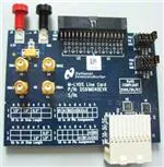
Figure 1 below represents the top layer drawing of the board with the silkscreen annotations. It is a 4 x 3 inch
10 layer printed circuit board (PCB) that features two DS91M040 (U1-U2) devices.
MDE
FSEN2
MDE
FSEN2
FSEN1
DE
2
© 2008, National Semiconductor Corp.
FSEN1
RE*
April 14, 2008
Rev. 1.0
DE
RE*
Figure 1 - DS91M040EVK Top View Drawing
�Each device (U1 or U2) has four channels. The three M-LVDS channels of each device directly connect to the
first two rows of J4, which is an ADF (Advanced Differential Fabric) connector. When J4 is inserted into any
ATCA backplane slot (location J20/P20 for those of you familiar with ATCA backplanes), the M-LVDS I/O pins of
each device electrically connect to one of the clock busses (there are six clock busses in an ATCA backplane –
See Figure 2).
The remaining M-LVDS channel of each device connects to the SMA connectors for device standalone
evaluation or evaluation in point-to-point links.
Table 1 provides M-LVDS I/O pin to J4 pin (and stub length) or SMA connector mapping and LVCMOS pins to
J2 pin mapping.
Device
U1
U1
U1
U1
U2
U2
U2
U2
M-LVDS Pins
A0
B0
A1
B1
A2
B2
A3
B3
A0
B0
A1
B1
A2
B2
A3
B3
J4 Pins / SMA Connector
SMA1
SMA2
B1
A1
D1
C1
F1
E1
G1
H1
E2
F2
G2
H2
SMA3
SMA4
Stub Length
NA
1.50”
1.00”
0.50”
0.50”
1.00”
1.50”
NA
LVCMOS Pins
R0
D0
R1
D1
R2
D2
R3
D3
R0
D0
R1
D1
R2
D2
R3
D3
J2 Pins
1
3
5
7
9
11
13
15
17
19
21
23
25
27
29
31
Table 1 - U1 and U2 Pin to Connector Pin Mapping
J1 provides easy connection to U1 control pins. Refer to the DS91M040 datasheet for the device pin
descriptions.
J3 provides easy connection to U2 control pins. Refer to the DS91M040 datasheet for the device pin
descriptions.
J5 and J6 are power and ground connections.
April 14, 2008
Rev. 1.0
3
© 2008, National Semiconductor Corp.
�DS91M040 Evaluation in an ATCA Backplane
The following is a recommended procedure for building an evaluation M-LVDS clock distribution network with
DS91M040EVK evaluation boards. The assumption is that the user already has an ATCA backplane. Figure 2
depicts configuration of a generic M-LVDS clock network in an ATCA backplane.
1. Use two or more DS91M040 evaluation boards and install them at backplane location J20/P20, in the
desired slots.
2. Apply the power to the boards (3.3V typical) between J5 and J6 banana plug receptacles, observe the
value of ICC, and compare it with the expected value (refer to the datasheet) to ensure that the devices
are functional.
3. Select the board you want to configure as a clock driver/distributor. This is accomplished by setting DE
and RE* pins to VDD (J1 or J3). Set MDE pin to VDD. Connect a clock source to one of the driver
inputs (J2).
4. Configure the remaining boards as clock receivers. This is accomplished by setting DE and RE* pins to
GND (J1 or J3). Set MDE pin to VDD. Set the receiver to either M-LVDS Type 1 (FSEN pins set to
GND) or Type 2 (FSEN pins set to VDD).
5. Observe clock waveforms by either connecting receiver LVCMOS output pins (J2) directly to an
oscilloscope or by probing receiver M-LVDS input pins with a differential probe.
Figure 2 - M-LVDS Clock Distribution Network in an ATCA Backplane
April 14, 2008
Rev. 1.0
4
© 2008, National Semiconductor Corp.
�The block diagram of Figure 2 details a clock distribution network in an ATCA backplane. The clock busses
have 130-ohm differential impedance and are doubly terminated with 80 ohms at either end of the backplane.
The parallel combination of 80-ohm resistors means that the MLVDS devices will be driving a 40-ohm load
termination. The maximum stub length from the backplane is defined in the ATCA standard as 1 inch or 2.54
cm.
Figure 3 shows a picture of a 14-slot ATCA backplane fully populated with DS91M040 evaluation boards.
Figure 3 - DS91M040 Evaluation Boards in an ATCA Backplane
April 14, 2008
Rev. 1.0
5
© 2008, National Semiconductor Corp.
�Figure 4 shows 19.44 MHz clock waveforms obtained with a differential probe, Tektronix P6330, on the M-LVDS
input pins of the device on a receiver board in slot #8. The14-slot backplane was fully populated. The clock
driver/distributor board was in slot #7.
Figure 4 - 19.44 MHz Clock Waveforms Show Stub Length Effects on Signal Integrity
April 14, 2008
Rev. 1.0
6
© 2008, National Semiconductor Corp.
�DS91M040 Evaluation in a Point-to-Point Link
The following is a recommended procedure for building an evaluation M-LVDS point-point network with
DS91M040 evaluation boards. Figure 5 depicts a typical setup and instrumentation used for evaluation of a
point-to-point link.
1. Use a single DS91M040 evaluation board.
2. Apply the power to the board (3.3 V typical) between J5 and J6 banana plug receptacles, observe the
value of ICC, and compare it with the expected value (refer to the datasheet) to ensure that the devices
are functional.
3. Configure U1 as a driver. This is accomplished by setting DE and RE* pins to VDD (J1). Connect a
signal source to the driver inputs (J2, pin 3).
4. Configure U2 as a receiver. This is accomplished by setting DE and RE* pins to GND (J3).
5. Select a differential interconnect with balanced 100-ohm differential impedance (i.e. UTP cable) and
connect the M-LVDS pins of both devices through SMA connectors (SMA1 and SMA2 for U1 driver
outputs; SMA3 and SMA4 for U2 receiver inputs ;). You may want to consider developing / obtaining an
SMA to RJ45 adapter board for easy interface from SMA connectors to twisted pair cables. See the
following link: http://www.national.com/appinfo/lvds/sma2rj45evk.html.
6. Terminate the interconnect with a matching resistor on the inputs of the U2 receiver (R2).
7. Observe waveforms by either connecting the receiver LVCMOS output pin (J2, pin 29) directly to an
oscilloscope or by probing receiver M-LVDS input pins with a differential probe.
Figure 5 - M-LVDS Point-to-Point Link with DS91M040 Boards and UTP Cable
April 14, 2008
Rev. 1.0
7
© 2008, National Semiconductor Corp.
�Figure 6 shows eye diagrams acquired at the output of the DS91M040 driver loaded with a 100-ohm resistor
and after 50 m CAT5e cable terminated with a 100-ohm resistor. The generator connected to the driver input
simulated a 100 Mbps PRBS-7 NRZ.
Figure 6 - Eye Diagram Before and After 50m of CAT5e
April 14, 2008
Rev. 1.0
8
© 2008, National Semiconductor Corp.
�IMPORTANT NOTICE
Texas Instruments Incorporated and its subsidiaries (TI) reserve the right to make corrections, modifications, enhancements, improvements,
and other changes to its products and services at any time and to discontinue any product or service without notice. Customers should
obtain the latest relevant information before placing orders and should verify that such information is current and complete. All products are
sold subject to TI’s terms and conditions of sale supplied at the time of order acknowledgment.
TI warrants performance of its hardware products to the specifications applicable at the time of sale in accordance with TI’s standard
warranty. Testing and other quality control techniques are used to the extent TI deems necessary to support this warranty. Except where
mandated by government requirements, testing of all parameters of each product is not necessarily performed.
TI assumes no liability for applications assistance or customer product design. Customers are responsible for their products and
applications using TI components. To minimize the risks associated with customer products and applications, customers should provide
adequate design and operating safeguards.
TI does not warrant or represent that any license, either express or implied, is granted under any TI patent right, copyright, mask work right,
or other TI intellectual property right relating to any combination, machine, or process in which TI products or services are used. Information
published by TI regarding third-party products or services does not constitute a license from TI to use such products or services or a
warranty or endorsement thereof. Use of such information may require a license from a third party under the patents or other intellectual
property of the third party, or a license from TI under the patents or other intellectual property of TI.
Reproduction of TI information in TI data books or data sheets is permissible only if reproduction is without alteration and is accompanied
by all associated warranties, conditions, limitations, and notices. Reproduction of this information with alteration is an unfair and deceptive
business practice. TI is not responsible or liable for such altered documentation. Information of third parties may be subject to additional
restrictions.
Resale of TI products or services with statements different from or beyond the parameters stated by TI for that product or service voids all
express and any implied warranties for the associated TI product or service and is an unfair and deceptive business practice. TI is not
responsible or liable for any such statements.
TI products are not authorized for use in safety-critical applications (such as life support) where a failure of the TI product would reasonably
be expected to cause severe personal injury or death, unless officers of the parties have executed an agreement specifically governing
such use. Buyers represent that they have all necessary expertise in the safety and regulatory ramifications of their applications, and
acknowledge and agree that they are solely responsible for all legal, regulatory and safety-related requirements concerning their products
and any use of TI products in such safety-critical applications, notwithstanding any applications-related information or support that may be
provided by TI. Further, Buyers must fully indemnify TI and its representatives against any damages arising out of the use of TI products in
such safety-critical applications.
TI products are neither designed nor intended for use in military/aerospace applications or environments unless the TI products are
specifically designated by TI as military-grade or "enhanced plastic." Only products designated by TI as military-grade meet military
specifications. Buyers acknowledge and agree that any such use of TI products which TI has not designated as military-grade is solely at
the Buyer's risk, and that they are solely responsible for compliance with all legal and regulatory requirements in connection with such use.
TI products are neither designed nor intended for use in automotive applications or environments unless the specific TI products are
designated by TI as compliant with ISO/TS 16949 requirements. Buyers acknowledge and agree that, if they use any non-designated
products in automotive applications, TI will not be responsible for any failure to meet such requirements.
Following are URLs where you can obtain information on other Texas Instruments products and application solutions:
Products
Applications
Audio
www.ti.com/audio
Automotive and Transportation www.ti.com/automotive
Amplifiers
amplifier.ti.com
Communications and Telecom www.ti.com/communications
Data Converters
dataconverter.ti.com
Computers and Peripherals
www.ti.com/computers
DLP® Products
www.dlp.com
Consumer Electronics
www.ti.com/consumer-apps
DSP
dsp.ti.com
Energy and Lighting
www.ti.com/energy
Clocks and Timers
www.ti.com/clocks
Industrial
www.ti.com/industrial
Interface
interface.ti.com
Medical
www.ti.com/medical
Logic
logic.ti.com
Security
www.ti.com/security
Power Mgmt
power.ti.com
Space, Avionics and Defense
www.ti.com/space-avionics-defense
Microcontrollers
microcontroller.ti.com
Video and Imaging
www.ti.com/video
RFID
www.ti-rfid.com
OMAP Mobile Processors
www.ti.com/omap
Wireless Connectivity
www.ti.com/wirelessconnectivity
TI E2E Community Home Page
e2e.ti.com
Mailing Address: Texas Instruments, Post Office Box 655303, Dallas, Texas 75265
Copyright © 2012, Texas Instruments Incorporated
�