User's Guide
SBOU153A – May 2015 – Revised November 2015
INA250AxEVM User's Guide
This user’s guide describes the characteristics, operation, and use of the INA250AxEVM evaluation
module. It discusses how to set up and configure the hardware and reviews various aspects of the
hardware operation. Throughout this document, the terms evaluation board, evaluation module, and EVM
are synonymous with the INA250AxEVM. This document also includes an electrical schematic, printed
circuit board (PCB) layout drawings, and a parts list for the EVM. NOTE: This user guide is for the new
revision of the EVM board. For users of the original-version EVM board, see the previous EVM user's
guide, SBOU153.
All trademarks are the property of their respective owners.
SBOU153A – May 2015 – Revised November 2015
Submit Documentation Feedback
Copyright © 2015, Texas Instruments Incorporated
INA250AxEVM User's Guide
1
�www.ti.com
1
2
3
Contents
Overview ..................................................................................................................... 3
1.1
INA250EVM Kit Contents .......................................................................................... 3
1.2
Related Documentation from Texas Instruments ............................................................... 3
Hardware...................................................................................................................... 4
2.1
Theory of Operation ................................................................................................ 4
2.2
Features .............................................................................................................. 5
2.3
Quick-Start Setup and Use ........................................................................................ 5
2.4
Current Input ........................................................................................................ 5
Schematic, PCB Layout, and Bill of Materials ........................................................................... 6
3.1
Schematic ............................................................................................................ 6
3.2
PCB Layout .......................................................................................................... 7
3.3
Bill of Materials .................................................................................................... 10
List of Figures
1
INA250Ax Test Board Block Diagram ..................................................................................... 4
2
INA250Ax Test Board Schematic .......................................................................................... 6
3
PCB Component Placement
4
PCB Top Layer ............................................................................................................... 8
5
PCB Bottom Layer ........................................................................................................... 9
...............................................................................................
7
List of Tables
2
1
INA250AxEVM Kit Contents ................................................................................................ 3
2
Related Documentation ..................................................................................................... 3
3
INA250Ax Test Board BOM
INA250AxEVM User's Guide
..............................................................................................
10
SBOU153A – May 2015 – Revised November 2015
Submit Documentation Feedback
Copyright © 2015, Texas Instruments Incorporated
�Overview
www.ti.com
1
Overview
The INA250 is a family of voltage-output current-shunt monitors that integrate an internal shunt resistor to
enable high-accuracy current measurements. The INA250 family of devices consists of the INA250A1,
INA250A2, INA250A3, and INA250A4 (all referred to as INA250Ax).
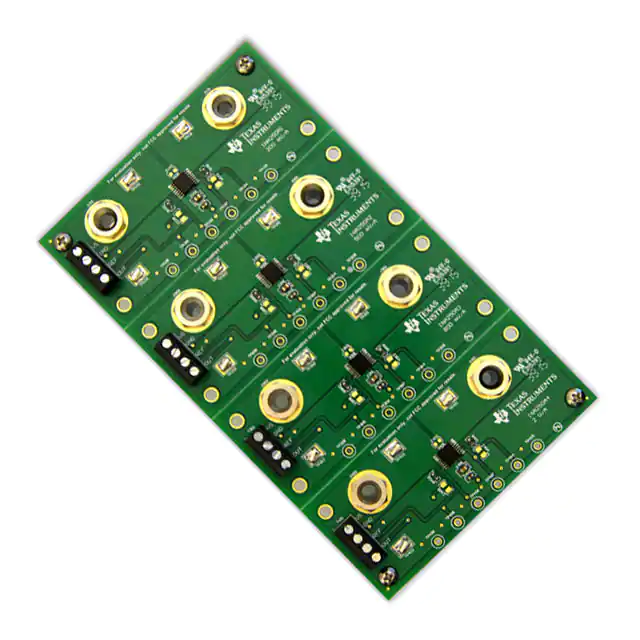
The INA250AxEVM consists of one PCB with an option to cut out four individual PCBs. Each of the PCB
cutouts consists of the INA250Ax device (where Ax is A1, A2, A3 and A4, for boards 1 through 4,
respectively), banana-jack terminals, screw terminals, and test points for external hardware connections.
1.1
INA250EVM Kit Contents
Table 1 summarizes the contents of the INA250EVM kit. Contact the Texas Instruments Product
Information Center nearest you if any component is missing. It is highly recommended that you also check
the INA250 device product folder on the TI web site at www.ti.com for any further information regarding
this product.
Table 1. INA250AxEVM Kit Contents
1.2
Item
Quantity
INA250 test board
1
Related Documentation from Texas Instruments
The following document provides information regarding Texas Instruments' integrated circuits used in the
assembly of the INA250AxEVM. This user's guide is available from the TI web site under literature number
SBOU153. Any letter appended to the literature number corresponds to the document revision that is
current at the time of the writing of this document. Newer revisions are be available from www.ti.com, or
call the Texas Instruments' Literature Response Center at (800) 477-8924 or the Product Information
Center at (972) 644-5580. When ordering, identify the document by both title and literature number.
Table 2. Related Documentation
Document
Literature Number
INA250 product data sheet
SBOS511
SBOU153A – May 2015 – Revised November 2015
Submit Documentation Feedback
Copyright © 2015, Texas Instruments Incorporated
INA250AxEVM User's Guide
3
�Hardware
2
www.ti.com
Hardware
Each of the PCBs on the INA250AxEVM requires a 2.7-V to 36-V power supply connected between the
VS and GND screw terminals. Alternately, the power supply can also be connected between test points
TPx08 (VS) and TPx03 (GND) or TPx09 (GND).
The INA250Ax family of devices have an integrated shunt of value 2 mΩ between the SH+ and SH– pins.
Connect a –0.1-V to +36-V supply in series with banana plugs Jx01 (IN+) and Jx02 (IN–), or test points
TPx01 (IN+) and TPx02 (IN–), to provide a path for current flowing through the integrated shunt resistor.
Use a voltmeter on the OUT screw terminal or test point TPx07 to measure the voltage output of the
INA250Ax.
For the following components, x = 1 to 4.
Cx01 and Cx02 are supply bypass capacitors for the INA250Ax.
Rx01 is a 0-Ω resistor that ties SH+ to VIN+.
Rx02 is a 0-Ω resistor that ties SH– to VIN–.
Components Rx01, Rx02, Cx03, Cx04, and Cx05 can be added or replaced to provide optional filtering of
the voltages out of the SH+ and SH– pins, and into the VIN+ and VIN– pins of the INA250Ax.
2.1
Theory of Operation
A block diagram of the INA250Ax test board hardware is shown in Figure 1.The INA250Ax test board
contains a four-port, screw terminal block to connect to the supply (VS), ground (GND), reference (REF)
and output (OUT) pins of the INA250Ax. There are ten test points located on each of the four PCB boards
that access the IN+ (TPx01), IN– (TPx02), VIN+ (TPx04), VIN– (TPx05), REF (TPx06), OUT (TPx07), VS
(TPx08), and GND (TPx03 and TPx09) pins of the device. Minimal support circuitry is included on the
PCB, and can be removed or bypassed as needed.
2.7 V to 36 V
INA250
Supply
(±0.1 V to +36 V)
CBYPASS
0.1 F
VS
IN+
IN±
SH+
SH±
VIN+
VIN±
±
+
LOAD
REF
OUT
GND
NOTE: One block diagram shown for all four EVM boards. Block diagram is functionally equivalent for all four EVM
boards.
Figure 1. INA250Ax Test Board Block Diagram
4
INA250AxEVM User's Guide
SBOU153A – May 2015 – Revised November 2015
Submit Documentation Feedback
Copyright © 2015, Texas Instruments Incorporated
�Hardware
www.ti.com
2.2
Features
The INA250AxEVM provides basic functional evaluation of this device family. The fixture layout is not
intended for electromagnetic compatibility (EMC) testing.
The INA250AxEVM PCB provides the following features:
• Ease of access to device pins with test points
• Multiple signal connection options
• Board layout and construction that supports 15-A current through the device across the full –40°C to
+125°C temperature range (see Section 3.2)
• Unpopulated component pads for optional input filtering with differential filter capacitor option included
Refer to the INA250 product data sheet, SBOS511, for comprehensive information about this family of
current sense amplifiers.
2.3
Quick-Start Setup and Use
Follow these procedures to setup and use the INA250EVM:
1. Connect an external dc supply voltage between 2.7 V and 36 V to the VS screw terminal or test point
TPx08, and connect the ground reference of that supply to the GND screw terminal or test point TPx03
or TPx09.
2. Connect an external dc supply voltage between 0 V and 18 V (referenced to the ground of the
INA250Ax) to the REF screw terminal or test point TPx06.
3. Connect a current source across the Jx01 and Jx02 banana jacks, or across the IN+ (TPx01) and IN–
(TPx02) test points, to provide current flowing through the integrated 2-mΩ shunt resistor. The
common-mode voltage on the IN+ and IN– pins must be between –0.1 V and +36 V (referenced to the
GND pin).
2.4
Current Input
The current flowing across the IN+ and IN– pins develops a differential voltage across the 2-mΩ shunt and
is amplified by the current shunt amplifier. The current flowing across this integrated shunt is multiplied by
the current gain of the INA250A1 (200 mV/A), INA250A2 (500 mV/A), INA250A3 (800 mV/A) or INA250A4
(2 V/A). Do not use this integrated shunt resistor as a stand-alone component. See the Integrated Shunt
Resistor section of the INA250 data sheet (SBOS511) for more information.
SBOU153A – May 2015 – Revised November 2015
Submit Documentation Feedback
Copyright © 2015, Texas Instruments Incorporated
INA250AxEVM User's Guide
5
�Schematic, PCB Layout, and Bill of Materials
www.ti.com
3
Schematic, PCB Layout, and Bill of Materials
3.1
Schematic
Figure 2 shows the complete schematic of the INA250Ax test board. Components Rx01, Rx02, Cx03,
Cx04, and Cx05 can be optionally added and replaced for an input filter. Keep the filter resistors to under
10 Ω to avoid excessive additional gain error. Banana jack terminals Jx01 and Jx02 give access to the IN+
and IN– pins, respectively. The VS, GND, REF, and OUT pins are accessed through screw terminal block
Tx01, or through test points TPx08, TPx03 or TPx09, TPx06 and TPx07, respectively. All pins except for
the shunt resistor Kelvin-connection pins (SH+ and SH–) are accessible using test points. The SH+ and
SH– pins are initially shorted to VIN+ and VIN– using 0-Ω resistors Rx01 and Rx02, respectively.
J101
108-0740-001
C103
TP101
J102
J201
J202
108-0740-001
108-0740-001
TP102
108-0740-001
C203
TP201
DNP
TP104
16
15
14
DNP
12
R101
GND1
VS1
0
T101
REF1
1
2
3
4
TP106
DNP
U101
C104
13
7
10
IN+
IN+
IN+
INININ-
VIN+
VIN-
GND1
TP105
1
2
3
DNP
5
R102
SH-
REF
OUT
9
VS
GND
GND
GND
6
8
11
SH+
TP204
C105
4
REF1
OUT1
ED555/4DS
GND1
16
15
14
DNP
12
R201
GND2
0
T201
OUT1
REF2
1
2
3
4
TP107
TP206
13
7
10
IN+
IN+
IN+
INININ-
VIN+
VIN-
ED555/4DS
GND2
TP205
1
2
3
C205
DNP
5
R202
SH-
4
REF
OUT
9
VS
GND
GND
GND
6
8
11
SH+
REF2
OUT2
OUT2
TP207
TP208
TP203
C202
TP109
TP209
0.1µF
C101
VS1
0.1µF
C201
VS2
1µF
1µF
GND1
GND2
J301
108-0740-001
C303
TP301
J302
J401
J402
108-0740-001
108-0740-001
TP302
108-0740-001
C403
TP401
DNP
TP304
16
15
14
DNP
12
R301
GND3
VS3
0
T301
1
2
3
4
ED555/4DS
REF3
TP306
13
7
10
IN+
IN+
IN+
INININ-
VIN+
VIN-
SH+
SH-
REF
OUT
VS
GND
GND
GND
REF3
OUT3
TP305
1
2
3
TP308
TP404
C305
DNP
5
R302
4
OUT3
6
8
11
GND3
16
15
14
DNP
12
R401
GND4
TP307
0
T401
1
2
3
4
ED555/4DS
REF4
TP406
13
7
10
IN+
IN+
IN+
INININ-
VIN+
VIN-
SH+
SH-
REF
OUT
VS
GND
GND
GND
REF4
OUT4
TP405
1
2
3
C405
DNP
5
R402
4
OUT4
6
8
11
TP408
TP407
TP403
C402
TP309
VS3
GND4
0
9
INA250A4PWR
GND4
TP303
C302
U401
C404
VS4
0
9
INA250A3PWR
GND3
TP402
DNP
U301
C304
GND2
0
INA250A2PWR
TP103
C102
U201
C204
VS2
0
INA250A1PWR
TP108
TP202
TP409
0.1µF
C301
VS4
1µF
0.1µF
C401
1µF
GND3
GND4
Figure 2. INA250Ax Test Board Schematic
6
INA250AxEVM User's Guide
SBOU153A – May 2015 – Revised November 2015
Submit Documentation Feedback
Copyright © 2015, Texas Instruments Incorporated
�Schematic, PCB Layout, and Bill of Materials
www.ti.com
3.2
PCB Layout
Figure 3 shows the component placement on the top layer of the test board. The two-layer EVM PCB
measures 3.2-in × 5.5-in and is fabricated with a 1-oz copper pour. The bottom layer has no components
but contains a solid copper ground plane that provides a low-impedance path for return currents.
The top layer of the PCB consists of power planes tied to the IN+ and IN– pins. These power planes are
approximately 1.472-in × 0.553-in each. The INA250 is rated to support a 10-A continuous current over
temperature. Enhance the current handling capability by using proper layout techniques that facilitate heat
dissipation. Combine the large power planes at the IN+ and IN– pins. Use a 2-oz copper pour to improve
the heat-dissipation capabilities, and thus increase the continuous-load current capacity.
Using the INA250AxEVM board with this robust layout and airflow, the INA250 device safely
accommodates up to 15 A of current over the entire –40°C to +125°C temperature range. Figure 4 and
Figure 5 show the top and bottom layers, respectively, of the test board.
Figure 3. PCB Component Placement
SBOU153A – May 2015 – Revised November 2015
Submit Documentation Feedback
Copyright © 2015, Texas Instruments Incorporated
INA250AxEVM User's Guide
7
�Schematic, PCB Layout, and Bill of Materials
www.ti.com
Figure 4. PCB Top Layer
8
INA250AxEVM User's Guide
SBOU153A – May 2015 – Revised November 2015
Submit Documentation Feedback
Copyright © 2015, Texas Instruments Incorporated
�Schematic, PCB Layout, and Bill of Materials
www.ti.com
Figure 5. PCB Bottom Layer
SBOU153A – May 2015 – Revised November 2015
Submit Documentation Feedback
Copyright © 2015, Texas Instruments Incorporated
INA250AxEVM User's Guide
9
�Schematic, PCB Layout, and Bill of Materials
3.3
www.ti.com
Bill of Materials
Table 3 lists the bill of materials (BOM) for the INA250 test board.
Table 3. INA250Ax Test Board BOM
Quantity
RefDes
4
C101, C201, C301,
C401
CAP, CERM, 1uF, 50V, +/-10%, X7R, 0805
CL21B105KBFNNNE
Samsung ElectroMechanics America, Inc
4
C102, C202, C302,
C402
CAP, CERM, 0.1uF, 50V, +/-10%, X7R, 0603
C1608X7R1H104K080AA
TDK Corporation
4
C103, C203, C303,
C403
CAP, CERM, 0.1uF, 25V, +/-10%, X5R, 0603
06033D104KAT2A
AVX
8
C104, C105, C204,
C205, C304, C305,
C404, C405
CAP, CERM, 0.1uF, 25 V, +/-10%, X7R, 0805
08053C104KAT2A
AVX
24
TP104, TP105,
TP106, TP107,
TP108, TP109,
TP204, TP205,
TP206, TP207,
TP208, TP209,
TP304, TP305,
TP306, TP307,
TP308, TP309,
TP404, TP405,
TP406, TP407,
TP408, TP409
Test Point, Multipurpose, White, TH
5012
Keystone
8
J101, J102, J201,
J202, J301, J302,
J401, J402
Standard Banana Jack, Uninsulated, 15A
108-0740-001
Emerson Network
Power
8
R101, R102, R201,
R202, R301, R302,
R401, R402
RES, 0 ohm, 0603
ERJ-3GEY0R00V
Panasonic Electronic
Components
4
T101, T201, T301,
T401
Terminal Block, 6A, 3.5mm Pitch, 4-Pos, TH
ED555/4DS
On-Shore Technology
12
TP101, TP102,
TP103, TP201,
TP202, TP203,
TP301, TP302,
TP303, TP401,
TP402, TP403
Test Point, Compact, SMT
5016
Keystone
1
U101
36-V, Low- or High-Side, Bidirectional, Zero-Drift Current-Shunt
Monitor with Precision Integrated Shunt Resistor, PW0016A
INA250A1PW
Texas Instruments
1
U201
36-V, Low- or High-Side, Bidirectional, Zero-Drift Current-Shunt
Monitor with Precision Integrated Shunt Resistor, PW0016A
INA250A2PW
Texas Instruments
1
U301
36-V, Low- or High-Side, Bidirectional, Zero-Drift Current-Shunt
Monitor with Precision Integrated Shunt Resistor, PW0016A
INA250A3PW
Texas Instruments
1
U401
36-V, Low- or High-Side, Bidirectional, Zero-Drift Current-Shunt
Monitor with Precision Integrated Shunt Resistor, PW0016A
INA250A4PW
Texas Instruments
10
Description
INA250AxEVM User's Guide
Part Number
Manufacturer
SBOU153A – May 2015 – Revised November 2015
Submit Documentation Feedback
Copyright © 2015, Texas Instruments Incorporated
�Revision History
www.ti.com
Revision History
Changes from Original (May 2015) to A Revision ........................................................................................................... Page
•
Changed user guide to include three additional devices (INA250A1, INA250A3, and INA250A4) to the existing
INA250A2. .................................................................................................................................. 1
NOTE: Page numbers for previous revisions may differ from page numbers in the current version.
SBOU153A – May 2015 – Revised November 2015
Submit Documentation Feedback
Copyright © 2015, Texas Instruments Incorporated
Revision History
11
�IMPORTANT NOTICE
Texas Instruments Incorporated and its subsidiaries (TI) reserve the right to make corrections, enhancements, improvements and other
changes to its semiconductor products and services per JESD46, latest issue, and to discontinue any product or service per JESD48, latest
issue. Buyers should obtain the latest relevant information before placing orders and should verify that such information is current and
complete. All semiconductor products (also referred to herein as “components”) are sold subject to TI’s terms and conditions of sale
supplied at the time of order acknowledgment.
TI warrants performance of its components to the specifications applicable at the time of sale, in accordance with the warranty in TI’s terms
and conditions of sale of semiconductor products. Testing and other quality control techniques are used to the extent TI deems necessary
to support this warranty. Except where mandated by applicable law, testing of all parameters of each component is not necessarily
performed.
TI assumes no liability for applications assistance or the design of Buyers’ products. Buyers are responsible for their products and
applications using TI components. To minimize the risks associated with Buyers’ products and applications, Buyers should provide
adequate design and operating safeguards.
TI does not warrant or represent that any license, either express or implied, is granted under any patent right, copyright, mask work right, or
other intellectual property right relating to any combination, machine, or process in which TI components or services are used. Information
published by TI regarding third-party products or services does not constitute a license to use such products or services or a warranty or
endorsement thereof. Use of such information may require a license from a third party under the patents or other intellectual property of the
third party, or a license from TI under the patents or other intellectual property of TI.
Reproduction of significant portions of TI information in TI data books or data sheets is permissible only if reproduction is without alteration
and is accompanied by all associated warranties, conditions, limitations, and notices. TI is not responsible or liable for such altered
documentation. Information of third parties may be subject to additional restrictions.
Resale of TI components or services with statements different from or beyond the parameters stated by TI for that component or service
voids all express and any implied warranties for the associated TI component or service and is an unfair and deceptive business practice.
TI is not responsible or liable for any such statements.
Buyer acknowledges and agrees that it is solely responsible for compliance with all legal, regulatory and safety-related requirements
concerning its products, and any use of TI components in its applications, notwithstanding any applications-related information or support
that may be provided by TI. Buyer represents and agrees that it has all the necessary expertise to create and implement safeguards which
anticipate dangerous consequences of failures, monitor failures and their consequences, lessen the likelihood of failures that might cause
harm and take appropriate remedial actions. Buyer will fully indemnify TI and its representatives against any damages arising out of the use
of any TI components in safety-critical applications.
In some cases, TI components may be promoted specifically to facilitate safety-related applications. With such components, TI’s goal is to
help enable customers to design and create their own end-product solutions that meet applicable functional safety standards and
requirements. Nonetheless, such components are subject to these terms.
No TI components are authorized for use in FDA Class III (or similar life-critical medical equipment) unless authorized officers of the parties
have executed a special agreement specifically governing such use.
Only those TI components which TI has specifically designated as military grade or “enhanced plastic” are designed and intended for use in
military/aerospace applications or environments. Buyer acknowledges and agrees that any military or aerospace use of TI components
which have not been so designated is solely at the Buyer's risk, and that Buyer is solely responsible for compliance with all legal and
regulatory requirements in connection with such use.
TI has specifically designated certain components as meeting ISO/TS16949 requirements, mainly for automotive use. In any case of use of
non-designated products, TI will not be responsible for any failure to meet ISO/TS16949.
Products
Applications
Audio
www.ti.com/audio
Automotive and Transportation
www.ti.com/automotive
Amplifiers
amplifier.ti.com
Communications and Telecom
www.ti.com/communications
Data Converters
dataconverter.ti.com
Computers and Peripherals
www.ti.com/computers
DLP® Products
www.dlp.com
Consumer Electronics
www.ti.com/consumer-apps
DSP
dsp.ti.com
Energy and Lighting
www.ti.com/energy
Clocks and Timers
www.ti.com/clocks
Industrial
www.ti.com/industrial
Interface
interface.ti.com
Medical
www.ti.com/medical
Logic
logic.ti.com
Security
www.ti.com/security
Power Mgmt
power.ti.com
Space, Avionics and Defense
www.ti.com/space-avionics-defense
Microcontrollers
microcontroller.ti.com
Video and Imaging
www.ti.com/video
RFID
www.ti-rfid.com
OMAP Applications Processors
www.ti.com/omap
TI E2E Community
e2e.ti.com
Wireless Connectivity
www.ti.com/wirelessconnectivity
Mailing Address: Texas Instruments, Post Office Box 655303, Dallas, Texas 75265
Copyright © 2015, Texas Instruments Incorporated
�