Sample &
Buy
Product
Folder
Support &
Community
Tools &
Software
Technical
Documents
LM25116
SNVS509E – APRIL 2007 – REVISED SEPTEMBER 2016
LM25116 Wide-Range Synchronous Buck Controller
1 Features
3 Description
•
•
•
•
•
•
•
•
•
•
•
•
•
•
•
The LM25116 is a synchronous buck controller
intended for step-down regulator applications from a
high voltage or widely varying input supply. The
control method is based upon current mode control
using an emulated current ramp. Current mode
control provides inherent line feedforward, cycle-bycycle current limiting and ease of loop compensation.
The use of an emulated control ramp reduces noise
sensitivity of the pulse-width modulation circuit,
allowing reliable control of very small duty cycles
necessary in high input voltage applications. The
operating frequency is programmable from 50 kHz to
1 MHz. The LM25116 drives external high-side and
low-side NMOS power switches with adaptive deadtime control. A user-selectable diode emulation mode
enables discontinuous mode operation for improved
efficiency at light load conditions. A low quiescent
current shutdown disables the controller and
consumes less than 10 µA of total input current.
Additional features include a high voltage bias
regulator, automatic switch-over to external bias for
improved efficiency, thermal shutdown, frequency
synchronization, cycle-by-cycle current limit and
adjustable line undervoltage lockout. The device is
available in a power enhanced 20-pin HTSSOP
package featuring an exposed die attach pad to aid
thermal dissipation.
1
Emulated Peak Current Mode
Wide Operating Range (Up to 42 V)
Low IQ Shutdown (< 10 µA)
Drives Standard or Logic Level MOSFETs
Robust 3.5-A Peak Gate Drive
Free-Run or Synchronous Operation to 1 MHz
Optional Diode Emulation Mode
Programmable Output From 1.215 V to 36 V
Precision 1.5% Voltage Reference
Programmable Current Limit
Programmable Soft Start
Programmable Line Undervoltage Lockout
Automatic Switch to External Bias Supply
20-Pin HTSSOP Exposed Pad
Thermal Shutdown
2 Applications
•
•
•
•
Automotive Infotainment
Industrial DC-DC Motor Drivers
Automotive USB Adapters
Telecom Servers
Device Information(1)
PART NUMBER
LM25116
PACKAGE
HTSSOP (20)
BODY SIZE (NOM)
6.50 mm × 4.40 mm
(1) For all available packages, see the orderable addendum at
the end of the data sheet.
Typical Application
VIN
LM25116
VIN
VCC
C VCC
CIN
RUV2
HB
UVLO
R UV1
VIN
CHB
HO
EN
L
VOUT
SW
CSYNC
RT/ SYNC
C OUT
LO
RT
CS
RS
CSG
COMP
C COMP
DEMB
CHF
R COMP
VOUT
FB
SS
C SS
RAMP
AGND PGND
C RAMP
VCCX
R FB2
RFB1
Copyright © 2016, Texas Instruments Incorporated
1
An IMPORTANT NOTICE at the end of this data sheet addresses availability, warranty, changes, use in safety-critical applications,
intellectual property matters and other important disclaimers. PRODUCTION DATA.
�LM25116
SNVS509E – APRIL 2007 – REVISED SEPTEMBER 2016
www.ti.com
Table of Contents
1
2
3
4
5
6
7
Features ..................................................................
Applications ...........................................................
Description .............................................................
Revision History.....................................................
Pin Configuration and Functions .........................
Specifications.........................................................
1
1
1
2
3
5
6.1
6.2
6.3
6.4
6.5
6.6
6.7
5
5
5
6
6
8
9
Absolute Maximum Ratings ......................................
ESD Ratings..............................................................
Recommended Operating Conditions.......................
Thermal Information ..................................................
Electrical Characteristics...........................................
Switching Characteristics ..........................................
Typical Characteristics ..............................................
Detailed Description ............................................ 13
7.1 Overview ................................................................. 13
7.2 Functional Block Diagram ....................................... 13
7.3 Feature Description................................................. 14
7.4 Device Functional Modes ....................................... 20
8
Application and Implementation ........................ 21
8.1 Application Information .......................................... 21
8.2 Typical Application .................................................. 21
9 Power Supply Recommendations...................... 32
10 Layout................................................................... 32
10.1 Layout Guidelines ................................................. 32
10.2 Layout Example .................................................... 33
11 Device and Documentation Support ................. 34
11.1
11.2
11.3
11.4
11.5
Receiving Notification of Documentation Updates
Community Resources..........................................
Trademarks ...........................................................
Electrostatic Discharge Caution ............................
Glossary ................................................................
34
34
34
34
34
12 Mechanical, Packaging, and Orderable
Information ........................................................... 34
4 Revision History
NOTE: Page numbers for previous revisions may differ from page numbers in the current version.
Changes from Revision D (February 2013) to Revision E
Page
•
Added ESD Ratings table, Feature Description section, Device Functional Modes, Application and Implementation
section, Power Supply Recommendations section, Layout section, Device and Documentation Support section, and
Mechanical, Packaging, and Orderable Information section .................................................................................................. 1
•
Changed RθJA value from 40 to 40.6 in the Thermal Information table .................................................................................. 6
•
Changed θJC value from 4 to 20.9 (RθJC(top)) and 1.7 (RθJC(bot)) in the Thermal Information table........................................... 6
Changes from Revision C (February 2013) to Revision D
•
2
Page
Changed layout of National Semiconductor Data Sheet to TI format .................................................................................... 1
Submit Documentation Feedback
Copyright © 2007–2016, Texas Instruments Incorporated
Product Folder Links: LM25116
�LM25116
www.ti.com
SNVS509E – APRIL 2007 – REVISED SEPTEMBER 2016
5 Pin Configuration and Functions
PWP Package
20-Pin HTSSOP
Top View
VIN
1
20
SW
UVLO
2
19
HO
RT/SYNC
3
18
HB
EN
4
17
VCCX
RAMP
5
16
VCC
EP
AGND
6
15
LO
SS
7
14
PGND
FB
8
13
CSG
COMP
9
12
CS
VOUT
10
11
DEMB
Not to scale
Pin Functions
PIN
NO.
1
NAME
VIN
TYPE (1)
DESCRIPTION
P
Chip supply voltage, input voltage monitor and input to the VCC regulator.
2
UVLO
I
If the UVLO pin is below 1.215 V, the regulator is in standby mode (VCC regulator running, switching
regulator disabled). If the UVLO pin voltage is above 1.215 V, the regulator is operational. An external
voltage divider can be used to set an undervoltage shutdown threshold. There is a fixed 5 µA pull up
current on this pin when EN is high. UVLO is pulled to ground in the event a current limit condition exists
for 256 clock cycles.
3
RT/SYNC
I
The internal oscillator is set with a single resistor between this pin and the AGND pin. The recommended
frequency range is 50 kHz to 1 MHz. The internal oscillator can be synchronized to an external clock by
AC coupling a positive edge onto this node.
4
EN
I
If the EN pin is below 0.5 V, the regulator is in a low power state drawing less than 10 µA from VIN. EN
must be pulled above 3.3 V for normal operation.
5
RAMP
I
Ramp control signal. An external capacitor connected between this pin and the AGND pin sets the ramp
slope used for current mode control.
6
AGND
G
Analog ground. Connect to PGND through the exposed pad ground connection under the LM25116.
7
SS
I
An external capacitor and an internal 10-µA current source set the soft start time constant for the rise of
the error amp reference. The SS pin is held low during VCC < 4.5 V, UVLO < 1.215 V, EN input low or
thermal shutdown.
8
FB
I
Feedback signal from the regulated output. This pin is connected to the inverting input of the internal error
amplifier. The regulation threshold is 1.215 V.
9
COMP
O
Output of the internal error amplifier. The loop compensation network must be connected between this pin
and the FB pin.
10
VOUT
I
Output monitor. Connect directly to the output voltage.
11
DEMB
I
Low-side MOSFET source voltage monitor for diode emulation. For start-up into a pre-biased load, tie this
pin to ground at the CSG connection. For fully synchronous operation, use an external series resistor
between DEMB and ground to raise the diode emulation threshold above the low-side SW on-voltage.
12
CS
I
Current sense amplifier input. Connect to the top of the current sense resistor or the drain of the lowsided MOSFET if RDS(ON) current sensing is used.
(1)
G = Ground, I = Input, O = Output, P= Power
Submit Documentation Feedback
Copyright © 2007–2016, Texas Instruments Incorporated
Product Folder Links: LM25116
3
�LM25116
SNVS509E – APRIL 2007 – REVISED SEPTEMBER 2016
www.ti.com
Pin Functions (continued)
PIN
NO.
NAME
TYPE (1)
DESCRIPTION
13
CSG
G
Current sense amplifier input. Connect to the bottom of the sense resistor or the source of the low-side
MOSFET if RDS(ON) current sensing is used.
14
PGND
G
Power ground. Connect to AGND through the exposed pad ground connection under the LM25116.
15
LO
O
Connect to the gate of the low-side synchronous MOSFET through a short, low inductance path.
16
VCC
P
Locally decouple to PGND using a low ESR/ESL capacitor placed as close to the controller as possible.
17
VCCX
P
Optional input for an externally supplied VCC. If VCCX > 4.5 V, VCCX is internally connected to VCC and
the internal VCC regulator is disabled. If VCCX is unused, it must be connected to ground.
18
HB
P
High-side driver supply for bootstrap gate drive. Connect to the cathode of the bootstrap diode and the
positive terminal of the bootstrap capacitor. The bootstrap capacitor supplies current to charge the highside MOSFET gate and must be placed as close to the controller as possible.
19
HO
O
Connect to the gate of the high-side synchronous MOSFET through a short, low inductance path
20
SW
O
Switch node. Connect to the negative terminal of the bootstrap capacitor and the source terminal of the
high-side MOSFET.
EP
EP
—
Exposed pad. Solder to ground plane.
4
Submit Documentation Feedback
Copyright © 2007–2016, Texas Instruments Incorporated
Product Folder Links: LM25116
�LM25116
www.ti.com
SNVS509E – APRIL 2007 – REVISED SEPTEMBER 2016
6 Specifications
6.1 Absolute Maximum Ratings
over operating free-air temperature range (unless otherwise noted) (1)
MIN
MAX
UNIT
–0.3
45
V
–0.3
16
V
–3
45
V
HB to SW
–0.3
16
V
HO to SW
–0.3
HB + 0.3
V
VOUT to GND
–0.3
45
V
–1
1
V
LO to GND
–0.3
VCC + 0.3
V
SS to GND
–0.3
7
V
FB to GND
–0.3
7
V
DEMB to GND
–0.3
VCC
V
RT to GND
–0.3
7
V
EN to GND
–0.3
45
V
150
°C
150
°C
VIN to GND
VCC, VCCX, UVLO to GND
(2)
SW, CS to GND
CSG to GND
Junction temperature, TJ
Storage temperature, Tstg
(1)
(2)
–55
Stresses beyond those listed under Absolute Maximum Ratings may cause permanent damage to the device. These are stress ratings
only, which do not imply functional operation of the device at these or any other conditions beyond those indicated under Recommended
Operating Conditions. Exposure to absolute-maximum-rated conditions for extended periods may affect device reliability.
These pins must not exceed VIN.
6.2 ESD Ratings
VALUE
V(ESD)
(1)
(2)
Electrostatic discharge
Human-body model (HBM), per ANSI/ESDA/JEDEC JS-001 (1)
±2000
Charged-device model (CDM), per JEDEC specification JESD22-C101 (2)
±750
UNIT
V
JEDEC document JEP155 states that 500-V HBM allows safe manufacturing with a standard ESD control process.
JEDEC document JEP157 states that 250-V CDM allows safe manufacturing with a standard ESD control process.
6.3 Recommended Operating Conditions
over operating free-air temperature range (unless otherwise noted)
MIN
VIN
NOM
MAX
UNIT
6
42
V
VCC, VCCX
4.75
15
V
HB to SW
4.75
15
V
DEMB to GND
–0.3
2
V
Junction temperature
–40
125
°C
Submit Documentation Feedback
Copyright © 2007–2016, Texas Instruments Incorporated
Product Folder Links: LM25116
5
�LM25116
SNVS509E – APRIL 2007 – REVISED SEPTEMBER 2016
www.ti.com
6.4 Thermal Information
LM25116
THERMAL METRIC (1)
PWP (HTSSOP)
UNIT
20 PINS
RθJA
Junction-to-ambient thermal resistance
40.6
°C/W
RθJC(top)
Junction-to-case (top) thermal resistance
20.9
°C/W
RθJB
Junction-to-board thermal resistance
17.7
°C/W
ψJT
Junction-to-top characterization parameter
0.5
°C/W
ψJB
Junction-to-board characterization parameter
17.4
°C/W
RθJC(bot)
Junction-to-case (bottom) thermal resistance
1.7
°C/W
(1)
For more information about traditional and new thermal metrics, see the Semiconductor and IC Package Thermal Metrics application
report.
6.5 Electrical Characteristics
The following conditions apply: TJ = 25°C, minimum and maximum limits apply over the junction temperature range of –40°C
to 125°C and are provided for reference only, VIN = 24 V, VCC = 7.4 V, VCCX = 0 V, EN = 5 V, RT = 16 kΩ, no load on LO
and HO (unless otherwise noted).
PARAMETER
TEST CONDITIONS
MIN
TYP
MAX
UNIT
VIN SUPPLY
IBIAS
VIN operating current
VCCX = 0 V
4.6
6.5
mA
IBIASX
VIN operating current
VCCX = 5 V
1
1.5
mA
ISTDBY
VIN shutdown current
EN = 0 V
1
10
µA
7.4
7.7
V
VCC REGULATOR
VCC(REG)
VCC regulation
7.1
VCC LDO mode turnoff
10.6
VCC regulation
VIN = 6 V
5
5.9
VCC sourcing current limit
VCC = 0 V
15
26
VCCX switch threshold
VCCX rising
4.3
VCCX switch hysteresis
ICCX = 10 mA
VCCX leakage
VCCX = 0 V
VCCX pulldown resistance
VCCX = 3 V
VCC undervoltage threshold
VCC rising
3.8
4.7
V
6.2
Ω
V
–200
nA
100
4.3
VCC undervoltage hysteresis
4.5
kΩ
4.7
0.2
HB – SW = 15 V
125
V
mA
0.25
VCCX switch RDS(ON)
HB DC bias current
4.5
V
6
V
V
200
µA
0.5
V
–3
1
µA
0
1
µA
EN INPUT
VIL max
EN input low threshold
VIH min
EN input high threshold
3.3
EN input bias current
VEN = 3 V
EN input bias current
VEN = 0.5 V
EN input bias current
VEN = 42 V
–7.5
–1
V
15
µA
UVLO THRESHOLDS
UVLO standby threshold
UVLO rising
UVLO threshold hysteresis
UVLO pullup current source
1.215
1.262
0.1
UVLO = 0 V
UVLO pulldown RDS(ON)
6
1.17
Submit Documentation Feedback
V
5.4
80
V
µA
210
Ω
Copyright © 2007–2016, Texas Instruments Incorporated
Product Folder Links: LM25116
�LM25116
www.ti.com
SNVS509E – APRIL 2007 – REVISED SEPTEMBER 2016
Electrical Characteristics (continued)
The following conditions apply: TJ = 25°C, minimum and maximum limits apply over the junction temperature range of –40°C
to 125°C and are provided for reference only, VIN = 24 V, VCC = 7.4 V, VCCX = 0 V, EN = 5 V, RT = 16 kΩ, no load on LO
and HO (unless otherwise noted).
PARAMETER
TEST CONDITIONS
MIN
TYP
MAX
8
11
14
UNIT
SOFT START
SS current source
SS = 0 V
SS diode emulation ramp disable
threshold
SS rising
SS to FB offset
FB = 1.25 V
SS output low voltage
Sinking 100 µA, UVLO = 0 V
3
µA
V
160
mV
45
mV
ERROR AMPLIFIER
VREF
FB reference voltage
Measured at FB pin, FB = COMP
FB input bias current
FB = 2 V
COMP sink and source current
AOL
DC gain
fBW
Unity gain bandwidth
1.195
1.215
1.231
V
15
500
nA
3
mA
80
dB
3
MHz
PWM COMPARATORS
tHO(OFF)
Forced HO off-time
tON(min)
Minimum HO on-time
320
VIN = 42 V, CRAMP = 50 pF
450
580
100
ns
ns
OSCILLATOR
fSW1
Frequency 1
RT = 16 kΩ
180
200
220
kHz
fSW2
Frequency 2
RT = 5 kΩ
480
535
590
kHz
1.191
1.215
1.239
V
3
3.5
4
V
RT output voltage
RT sync positive threshold
CURRENT LIMIT
VCS(TH)
Cycle-by-cycle sense voltage
threshold (CSG to CS)
VCCX = 0 V, RAMP = 0 V
94
110
126
mV
VCS(THX)
Cycle-by-cycle sense voltage
threshold (CSG to CS)
VCCX = 5 V, RAMP = 0 V
105
122
139
mV
CS bias current
CS = 42 V
1
µA
CS bias current
CS = 0 V
90
125
µA
CSG bias current
CSG = 0 V
90
125
Current limit fault timer
RT = 16 kΩ, 200 kHz, 256 clock cycles
–1
1.28
µA
ms
RAMP GENERATOR
IR1
RAMP current 1
VIN = 40 V, VOUT=10 V
150
180
220
µA
IR2
RAMP current 2
VIN = 10 V, VOUT = 10 V
21
28
35
µA
VOUT bias current
VOUT = 36 V
200
µA
RAMP output low voltage
VIN = 40 V, VOUT = 10 V
265
mV
–6
mV
DIODE EMULATION
SW zero cross threshold
DEMB output current
DEMB = 0 V, SS = 1.25 V
1.6
2.7
3.8
µA
DEMB output current
DEMB =0 V, SS = 2.8 V
28
38
48
µA
DEMB output current
DEMB = 0 V, SS = regulated by FB
45
65
85
µA
0.17
V
LO GATE DRIVER
VOLL
LO low-state output voltage
ILO = 10 mA
0.08
VOHL
LO high-state output voltage
ILO = -100 mA, VOHL = VCC – VLO
0.25
V
LO rise time
C-load = 1000 pF
18
ns
LO fall time
C-load = 1000 pF
12
ns
Peak LO source current
VLO = 0 V
1.8
A
IOHL
Submit Documentation Feedback
Copyright © 2007–2016, Texas Instruments Incorporated
Product Folder Links: LM25116
7
�LM25116
SNVS509E – APRIL 2007 – REVISED SEPTEMBER 2016
www.ti.com
Electrical Characteristics (continued)
The following conditions apply: TJ = 25°C, minimum and maximum limits apply over the junction temperature range of –40°C
to 125°C and are provided for reference only, VIN = 24 V, VCC = 7.4 V, VCCX = 0 V, EN = 5 V, RT = 16 kΩ, no load on LO
and HO (unless otherwise noted).
PARAMETER
IOLL
Peak LO sink current
TEST CONDITIONS
MIN
VLO = VCC
TYP
MAX
3.5
UNIT
A
HO GATE DRIVER
VOLH
HO low-state output voltage
IHO = 100 mA
0.17
VOHH
HO high-state output voltage
IHO = -100 mA, VOHH = VHB – VHO
0.45
V
HO rise time
C-load = 1000 pF
19
ns
13
ns
1
A
2.2
A
3
V
170
°C
15
°C
HO high-side fall time
C-load = 1000 pF
IOHH
Peak HO source current
VHO = 0 V
IOLH
Peak HO sink current
VHO = VCC
HB to SW undervoltage
0.27
V
THERMAL
TSD
Thermal shutdown
Rising
Thermal shutdown hysteresis
6.6 Switching Characteristics
over operating free-air temperature range (unless otherwise noted)
PARAMETER
TEST CONDITIONS
MIN
TYP
MAX
UNIT
LO fall to HO rise delay
C-load = 0
75
ns
HO fall to LO rise delay
C-load = 0
70
ns
8
Submit Documentation Feedback
Copyright © 2007–2016, Texas Instruments Incorporated
Product Folder Links: LM25116
�LM25116
www.ti.com
SNVS509E – APRIL 2007 – REVISED SEPTEMBER 2016
6.7 Typical Characteristics
Figure 1. Typical Application Circuit Efficiency
Figure 2. Driver Source Current vs VCC
Figure 3. Driver Dead-time vs Temperature
Figure 4. HO High RDS(ON) vs VCC
Figure 5. Driver Sink Current vs VCC
Figure 6. HO Low RDS(ON) vs VCC
Submit Documentation Feedback
Copyright © 2007–2016, Texas Instruments Incorporated
Product Folder Links: LM25116
9
�LM25116
SNVS509E – APRIL 2007 – REVISED SEPTEMBER 2016
www.ti.com
Typical Characteristics (continued)
10
Figure 7. LO High RDS(ON) vs VCC
Figure 8. EN Input Threshold vs Temperature
Figure 9. LO Low RDS(ON) vs VCC
Figure 10. HB to SW UVLO vs Temperature
Figure 11. Forced HO Off-time vs Temperature
VCCX = 5 V
Figure 12. HB DC Bias Current vs Temperature
Submit Documentation Feedback
Copyright © 2007–2016, Texas Instruments Incorporated
Product Folder Links: LM25116
�LM25116
www.ti.com
SNVS509E – APRIL 2007 – REVISED SEPTEMBER 2016
Typical Characteristics (continued)
Figure 13. Frequency vs RT
Figure 14. Error Amp Gain vs Frequency
Figure 15. Frequency vs Temperature
Figure 16. Error Amp Phase vs Frequency
Figure 17. Frequency vs Temperature
Figure 18. Current Limit Threshold vs Temperature
Submit Documentation Feedback
Copyright © 2007–2016, Texas Instruments Incorporated
Product Folder Links: LM25116
11
�LM25116
SNVS509E – APRIL 2007 – REVISED SEPTEMBER 2016
www.ti.com
Typical Characteristics (continued)
12
Figure 19. VIN Operating Current vs Temperature
Figure 20. VCC vs Temperature
Figure 21. VCC UVLO vs Temperature
Figure 22. VCC vs VIN
Figure 23. VCC vs ICC
Figure 24. VCCX Switch RDS(ON) vs VCCX
Submit Documentation Feedback
Copyright © 2007–2016, Texas Instruments Incorporated
Product Folder Links: LM25116
�LM25116
www.ti.com
SNVS509E – APRIL 2007 – REVISED SEPTEMBER 2016
7 Detailed Description
7.1 Overview
The LM25116 high-voltage switching regulator features all of the functions necessary to implement an efficient
high-voltage buck regulator using a minimum of external components. This easy-to-use regulator integrates highside and low-side MOSFET drivers capable of supplying peak currents of 2 A. The regulator control method is
based on current mode control using an emulated current ramp. Emulated peak current mode control provides
inherent line feedforward, cycle-by-cycle current limiting and ease of loop compensation. The use of an emulated
control ramp reduces noise sensitivity of the pulse-width modulation circuit, allowing reliable processing of the
very small duty cycles necessary in high input voltage applications. The operating frequency is user
programmable from 50 kHz to 1 MHz. An oscillator or synchronization pin allows the operating frequency to be
set by a single resistor or synchronized to an external clock. Fault protection features include current limiting,
thermal shutdown and remote shutdown capability. An undervoltage lockout input allows regulator shutdown
when the input voltage is below a user-selected threshold, and an enable function puts the regulator into an
extremely low current shutdown through the enable input. The 20-pin HTSSOP package features an exposed
pad to aid in thermal dissipation.
7.2 Functional Block Diagram
VIN
C IN
6V
42
V R
4.5V
1 VIN
+
-
VCC 16
7. 4 V
REGULATOR
EN
SLEEP
MODE
SHUTDOWN
1.215V
STANDBY
D2
HB 18
THERMAL
SHUTDOWN
5 PA
UVLO
LOGIC
C FT
HICCUP FAULT TIMER
256 CLOCK CYCLES
UVLO
DIS
CHB
VIN
DRIVER
HO 19
CLK
7 SS
10 PA
S
3V
R
PWM
CSS
C COMP
ERROR
AMP
1.6V
COMP
+
10 x RS V/A
LO 15
A =10
VOUT
Q2
CSNUB
COUT
R SNUB
RS
0.5V
CSG 13
SW
DIODE
EMULATION
CONTROL
VIN
OSCILLATOR
IR
RAMP
11
VOUT
10
R FB1
AGND
5
DEMB
R FB2
RAMP GENERATOR
I R = 5 PA / V x ( VIN - VOUT ) + 25 PA
RT
L1
CLK
CLK
3 RT/SYNC
Q1
20
CS 12
TRACK
SAMPLE
and
HOLD
SS
C SYNC
SW
VCC
DRIVER
R COMP
9
Q
ADAPTIVE
TIMER
CURRENT
LIMIT
8 FB
CHF
Q
1V
1.215 V
SYNC
C VCC
D1
4 EN
2 UVLO
R UV1
C VCCX
UVLO
EN
R UV2
VCCX
17
VCCX
LM25116
PGND
6
14
CRAMP
Copyright © 2016, Texas Instruments Incorporated
Submit Documentation Feedback
Copyright © 2007–2016, Texas Instruments Incorporated
Product Folder Links: LM25116
13
�LM25116
SNVS509E – APRIL 2007 – REVISED SEPTEMBER 2016
www.ti.com
7.3 Feature Description
7.3.1 High-Voltage Start-Up Regulator
The LM25116 contains a dual mode internal high-voltage start-up regulator that provides the VCC bias supply for
the PWM controller and a bootstrap gate drive for the high-side buck MOSFET. The input pin (VIN) can be
connected directly to an input voltage source as high as 42 V. For input voltages below 10.6 V, a low dropout
switch connects VCC directly to VIN. In this supply range, VCC is approximately equal to VIN. For VIN voltages
greater than 10.6 V, the low dropout switch is disabled and the VCC regulator is enabled to maintain VCC at
approximately 7.4 V. The wide operating range of 6 V to 42 V is achieved through the use of this dual mode
regulator.
Upon power up, the regulator sources current into the capacitor connected to the VCC pin. When the voltage at
the VCC pin exceeds 4.5 V and the UVLO pin is greater than 1.215 V, the output switch is enabled and a softstart sequence begins. The output switch remains enabled until VCC falls below 4.5 V, EN is pulled low, the
UVLO pin falls below 1.215 V, or the die temperature exceeds the thermal limit threshold.
VCCX
CVCCX
VOUT
SW
L
COUT
Figure 25. VCCX Bias Supply with Additional Inductor Winding
An output voltage derived bias supply can be applied to the VCCX pin to reduce the IC power dissipation. If the
bias supply voltage is greater than 4.5 V, the internal regulator essentially shuts off, reducing the IC power
dissipation. The VCC regulator series pass transistor includes a diode between VCC and VIN that must not be
forward biased in normal operation. For an output voltage between 5 V and 15 V, VOUT can be connected
directly to VCCX. For VOUT < 5 V, a bias winding on the output inductor can be added to VOUT. If the bias
winding can supply VCCX greater than VIN, an external blocking diode is required from the input power supply to
the VIN pin to prevent VCC from discharging into the input supply.
The output of the VCC regulator is current limited to 15 mA minimum. The VCC current is determined by the
MOSFET gate charge, switching frequency and quiescent current (see MOSFETs in the Typical Application). If
VCCX is powered by the output voltage or an inductor winding, the VCC current must be evaluated during startup to ensure that it is less than the 15 mA minimum current limit specification. If VCCX is powered by an external
regulator derived from VIN, there is no restriction on the VCC current.
VIN
1
VIN
0.1 PF
6
AGND
Figure 26. Input Blocking Diode for VCCX > VIN
In high-voltage applications, take extra care to ensure the VIN pin does not exceed the absolute maximum
voltage rating of 45 V. During line or load transients, voltage ringing on the VIN line that exceeds values listed in
Absolute Maximum Ratings can damage the IC. Both careful PCB layout and the use of quality bypass
capacitors placed close to the VIN and GND pins are essential.
14
Submit Documentation Feedback
Copyright © 2007–2016, Texas Instruments Incorporated
Product Folder Links: LM25116
�LM25116
www.ti.com
SNVS509E – APRIL 2007 – REVISED SEPTEMBER 2016
Feature Description (continued)
7.3.2 Enable
The LM25116 contains an enable function allowing a very low input current shutdown. If the enable pin is pulled
below 0.5 V, the regulator enters shutdown, drawing less than 10 µA from the VIN pin. Raising the EN input
above 3.3 V returns the regulator to normal operation. The maximum EN transition time for proper operation is
one switching period. For example, the enable rise time must be less than 4 µs for 250-kHz operation.
A 1-MΩ pullup resistor to VIN can be used to interface with an open collector control signal. At low input voltage
the pullup resistor may be reduced to 100 kΩ to speed up the EN transition time. The EN pin can be tied directly
to VIN if this function is not required. It must not be left floating. If low-power shutdown is not required, the UVLO
pin must be used as an on/off control.
Internal 5V rail
3 PA
EN
6V
Figure 27. Enable Circuit
Figure 28. EN Bias Current vs Voltage
Submit Documentation Feedback
Copyright © 2007–2016, Texas Instruments Incorporated
Product Folder Links: LM25116
15
�LM25116
SNVS509E – APRIL 2007 – REVISED SEPTEMBER 2016
www.ti.com
Feature Description (continued)
7.3.3 UVLO
An undervoltage lockout pin is provided to disable the regulator without entering shutdown. If the UVLO pin is
pulled below 1.215 V, the regulator enters a standby mode of operation with the soft-start capacitor discharged
and outputs disabled, but with the VCC regulator running. If the UVLO input is pulled above 1.215 V, the
controller resumes normal operation. A voltage divider from input to ground can be used to set a VIN threshold to
disable the supply in brown-out conditions or for low input faults. The UVLO pin has a 5-µA internal pullup
current that allows this pin to left open if the input undervoltage lockout function is not required. For applications
which require fast on or off cycling, the UVLO pin with an open collector control signal may be used to ensure
proper start-up sequencing.
The UVLO pin is also used to implement a hiccup current limit. If a current limit fault exists for more than 256
consecutive clock cycles, the UVLO pin is internally pulled down to 200 mV and then released, and a new SS
cycle initiated. A capacitor to ground connected to the UVLO pin sets the timing for hiccup mode current limit.
When this feature is used in conjunction with the voltage divider, a diode across the top resistor may be used to
discharge the capacitor in the event of an input undervoltage condition. There is a 5-µs filter at the input to the
fault comparator. At higher switching frequency (greater than approximately 250 kHz) the hiccup timer may be
disabled if the fault capacitor is not used.
7.3.4 Oscillator and Sync Capability
The LM25116 oscillator frequency is set by a single external resistor connected between the RT/SYNC pin and
the AGND pin. The resistor must be placed very close to the device and connected directly to the pins of the IC
(RT/SYNC and AGND). To set a desired oscillator frequency (fSW), the necessary value for the resistor can be
calculated from Equation 1.
RT =
T - 450 ns
284 pF
where
•
•
•
T = 1 / fSW
RT is in Ω
450 ns represents the fixed minimum off time
(1)
The LM25116 oscillator has a maximum programmable frequency that is dependent on the VCC voltage. If VCC
is above 6 V, the frequency can be programmed up to 1 MHz. If VCCX is used to bias VCC and VCCX < 6 V, the
maximum programmable oscillator frequency is 750 kHz.
The RT/SYNC pin can be used to synchronize the internal oscillator to an external clock. The external clock must
be a higher frequency than the free-running frequency set by the RT resistor. The internal oscillator can be
synchronized to an external clock by AC coupling a positive edge into the RT/SYNC pin. The voltage at the
RT/SYNC pin is nominally 1.215 V and must exceed 4 V to trip the internal synchronization pulse detection. A
5-V amplitude signal and 100-pF coupling capacitor are recommended. The free-running frequency must be set
nominally 15% below the external clock. Synchronizing above twice the free-running frequency may result in
abnormal behavior of the pulse width modulator.
7.3.5 Error Amplifier and PWM Comparator
The internal high-gain error amplifier generates an error signal proportional to the difference between the
regulated output voltage and an internal precision reference (1.215 V). The output of the error amplifier is
connected to the COMP pin allowing the user to provide loop compensation components, generally a type II
network. This network creates a pole at very low frequency, a mid-band zero, and a noise reducing high
frequency pole. The PWM comparator compares the emulated current sense signal from the RAMP generator to
the error amplifier output voltage at the COMP pin.
7.3.6 Ramp Generator
The ramp signal used in the pulse width modulator for current mode control is typically derived directly from the
buck switch current. This switch current corresponds to the positive slope portion of the inductor current. Using
this signal for the PWM ramp simplifies the control loop transfer function to a single pole response and provides
inherent input voltage feedforward compensation. The disadvantage of using the buck switch current signal for
PWM control is the large leading edge spike due to circuit parasitics that must be filtered or blanked. Also, the
16
Submit Documentation Feedback
Copyright © 2007–2016, Texas Instruments Incorporated
Product Folder Links: LM25116
�LM25116
www.ti.com
SNVS509E – APRIL 2007 – REVISED SEPTEMBER 2016
Feature Description (continued)
current measurement may introduce significant propagation delays. The filtering, blanking time and propagation
delay limit the minimal achievable pulse width. In applications where the input voltage may be relatively large in
comparison to the output voltage, controlling small pulse widths and duty cycles is necessary for regulation. The
LM25116 uses a unique ramp generator which does not actually measure the buck switch current but rather
reconstructs the signal. Representing or emulating the inductor current provides a ramp signal to the PWM
comparator that is free of leading edge spikes and measurement or filtering delays. The current reconstruction is
comprised of two elements, a sample-and-hold DC level and an emulated current ramp.
(5 PA/V x (VIN-VOUT) + 25 PA) x
tON
CRAMP
RAMP
Sample and Hold
DC Level
10 x RS V/A
tON
Figure 29. Composition of Current Sense Signal
The sample-and-hold DC level is derived from a measurement of the recirculating current through either the lowside MOSFET or current sense resistor. The voltage level across the MOSFET or sense resistor is sampled and
held just prior to the onset of the next conduction interval of the buck switch. The current sensing and sampleand-hold provide the DC level of the reconstructed current signal. The positive slope inductor current ramp is
emulated by an external capacitor connected from the RAMP pin to the AGND and an internal voltage controlled
current source. The ramp current source that emulates the inductor current is a function of the VIN and VOUT
voltages per Equation 2.
IR = 5 µA/V × (VIN – VOUT) + 25 µA
(2)
Proper selection of the RAMP capacitor (CRAMP) depends upon the value of the output inductor (L) and the
current sense resistor (RS). For proper current emulation, the DC sample and hold value and the ramp amplitude
must have the same dependence on the load current. That is in Equation 3.
RS x A =
CRAMP =
gm x L
, so
CRAMP
gm x L
A x RS
where
•
•
gm is the ramp generator transconductance (5 µA/V)
A is the current sense amplifier gain (10 V/V).
(3)
The ramp capacitor must be placed very close to the device and connected directly to the pins of the IC (RAMP
and AGND).
The difference between the average inductor current and the DC value of the sampled inductor current can
cause instability for certain operating conditions. This instability is known as subharmonic oscillation, which
occurs when the inductor ripple current does not return to its initial value by the start of next switching cycle.
Subharmonic oscillation is normally characterized by observing alternating wide and narrow pulses at the switch
node. Adding a fixed slope voltage ramp (slope compensation) to the current sense signal prevents this
oscillation. The 25 µA of offset current provided from the emulated current source adds the optimal slope
compensation to the ramp signal for a 5-V output. For higher output voltages, additional slope compensation may
be required. In these applications, a resistor is added between RAMP and VCC to increase the ramp slope
compensation.
Submit Documentation Feedback
Copyright © 2007–2016, Texas Instruments Incorporated
Product Folder Links: LM25116
17
�LM25116
SNVS509E – APRIL 2007 – REVISED SEPTEMBER 2016
www.ti.com
Feature Description (continued)
SW
LO
RG
CS
RG
CSG
DEMB
RDEMB
Figure 30. RDS(ON) Current Sensing without Diode Emulation
The DC current sample is obtained using the CS and CSG pins connected to either a source sense resistor (RS)
or the RDS(ON) of the low-side MOSFET. For RDS(ON) sensing, RS = RDS(ON) of the low-side MOSFET. In this case
it is sometimes helpful to adjust the current sense amplifier gain (A) to a lower value to obtain the desired current
limit. Adding external resistors RG in series with CS and CSG, the current sense amplifier gain A becomes
Equation 4.
A,
10k
1k + RG
(4)
7.3.7 Current Limit
The LM25116 contains a current limit monitoring scheme to protect the circuit from possible overcurrent
conditions. When set correctly, the emulated current sense signal is proportional to the buck switch current with a
scale factor determined by the current limit sense resistor. The emulated ramp signal is applied to the current
limit comparator. If the emulated ramp signal exceeds 1.6 V, the current cycle is terminated (cycle-by-cycle
current limiting). Because the ramp amplitude is proportional to VIN – VOUT, if VOUT is shorted, there is an
immediate reduction in duty cycle. To further protect the external switches during prolonged current limit
conditions, an internal counter counts clock pulses when in current limit. When the counter detects 256
consecutive clock cycles, the regulator enters a low power dissipation hiccup mode of current limit. The regulator
is shut down by momentarily pulling UVLO low, and the soft-start capacitor discharged. The regulator is restarted
with a full soft-start cycle once UVLO charges back to 1.215 V. This process is repeated until the fault is
removed. The hiccup off-time can be controlled by a capacitor to ground on the UVLO pin. In applications with
low output inductance and high input voltage, the switch current may overshoot due to the propagation delay of
the current limit comparator. If an overshoot must occur, the sample-and-hold circuit detects the excess
recirculating current. If the sample-and-hold DC level exceeds the internal current limit threshold, the buck switch
is disabled and skip pulses until the current has decayed below the current limit threshold. This approach
prevents current runaway conditions due to propagation delays or inductor saturation because the inductor
current is forced to decay following any current overshoot.
CURRENT SENSE
CURRENT LIMIT
COMPARATOR
AMPLIFIER
1.6V
-
10k
LO
1k
CS
RG
+
-RS
++
gm x (VIN - VOUT) + 25 PA
10k
1k
CSG
IL
RG
0.5V
HO
RAMP
A=
10k
1k + RG
CRAMP
Figure 31. Current Limit and Ramp Circuit
18
Submit Documentation Feedback
Copyright © 2007–2016, Texas Instruments Incorporated
Product Folder Links: LM25116
�LM25116
www.ti.com
SNVS509E – APRIL 2007 – REVISED SEPTEMBER 2016
Feature Description (continued)
Using a current sense resistor in the source of the low-side MOSFET provides superior current limit accuracy
compared to RDS(ON) sensing. RDS(ON) sensing is far less accurate due to the large variation of MOSFET RDS(ON)
with temperature and part-to-part variation. The CS and CSG pins must be Kelvin connected to the current sense
resistor or MOSFET drain and source.
The peak current which triggers the current limit comparator is calculated with Equation 5.
1.1V IPEAK =
25 PA x tON
CRAMP
A x RS
,
1.1V
A x RS
where
•
tON is the on-time of the high-side MOSFET
(5)
The 1.1-V threshold is the difference between the 1.6-V reference at the current limit comparator and the 0.5-V
offset at the current sense amplifier. This offset at the current sense amplifier allows the inductor ripple current to
go negative by 0.5 V / (A × RS) when running full synchronous operation.
Current limit hysteresis prevents chatter around the threshold when VCCX is powered from VOUT. When
4.5 V < VCC < 5.8 V, the 1.6-V reference is increased to 1.72 V. The peak current which triggers the current limit
comparator becomes Equation 6.
1.22V IPEAK =
25 PA x tON
CRAMP
A x RS
,
1.22V
A x RS
(6)
This has the effect of a 10% foldback of the peak current during a short circuit when VCCX is powered from a
5-V output.
7.3.8 HO Output
The LM25116 contains a high current, high-side driver and associated high-voltage level shift. This gate driver
circuit works in conjunction with an external diode and bootstrap capacitor. A 1-µF ceramic capacitor, connected
with short traces between the HB pin and SW pin, is recommended. During the off-time of the high-side
MOSFET, the SW pin voltage is approximately –0.5 V and the bootstrap capacitor charges from VCC through the
external bootstrap diode. When operating with a high PWM duty cycle, the buck switch is forced off each cycle
for 450 ns to ensure that the bootstrap capacitor is recharged.
The LO and HO outputs are controlled with an adaptive deadtime methodology which insures that both outputs
are never enabled at the same time. When the controller commands HO to be enabled, the adaptive block first
disables LO and waits for the LO voltage to drop below approximately 25% of VCC. HO is then enabled after a
small delay. Similarly, when HO turns off, LO waits until the SW voltage has fallen to ½ of VCC. LO is then
enabled after a small delay. In the event that SW does not fall within approximately 150 ns, LO is asserted high.
This methodology insures adequate dead-time for appropriately sized MOSFETs.
In some applications it may be desirable to slow down the high-side MOSFET turnon time to control switching
spikes. This may be accomplished by adding a resistor is series with the HO output to the high-side gate. Values
greater than 10 Ω must be avoided so as not to interfere with the adaptive gate drive. Use of an HB resistor for
this function must be carefully evaluated so as not cause potentially harmful negative voltage to the high-side
driver, and is generally limited to 2.2 Ω maximum.
7.3.9 Thermal Protection
Internal thermal shutdown circuitry is provided to protect the integrated circuit in the event the maximum junction
temperature is exceeded. When activated, typically at 170°C, the controller is forced into a low power reset state,
disabling the output driver and the bias regulator. This is designed to prevent catastrophic failures from
accidental device overheating.
Submit Documentation Feedback
Copyright © 2007–2016, Texas Instruments Incorporated
Product Folder Links: LM25116
19
�LM25116
SNVS509E – APRIL 2007 – REVISED SEPTEMBER 2016
www.ti.com
7.4 Device Functional Modes
7.4.1 Soft Start and Diode Emulation
The soft start feature allows the regulator to gradually reach the initial steady state operating point, thus reducing
start-up stresses and surges. The LM25116 regulates the FB pin to the SS pin voltage or the internal 1.215-V
reference, whichever is lower. At the beginning of the soft-start sequence when SS = 0 V, the internal 10-µA softstart current source gradually increases the voltage of an external soft-start capacitor (CSS) connected to the SS
pin resulting in a gradual rise of FB and the output voltage.
DIODE EMULATION
COMPARATOR
+
RS
RDEMB
SW
DEMB
1.215V
5V
40k
SS Latch
+
SS
-
Figure 32. Diode Emulation Control
During this initial charging of CSS to the internal reference voltage, the LM25116 forces diode emulation. That is,
the low-side MOSFET turns off for the remainder of a cycle if the sensed inductor current becomes negative. The
inductor current is sensed by monitoring the voltage between SW and DEMB. As the SS capacitor continues to
charge beyond 1.215 V to 3 V, the DEMB bias current increases from 0 µA up to 40 µA. With the use of an
external DEMB resistor (RDEMB), the current sense threshold for diode emulation increases resulting in the
gradual transition to synchronous operation. Forcing diode emulation during soft start allows the LM25116 to
start up into a prebiased output without unnecessarily discharging the output capacitor. Full synchronous
operation is obtained if the DEMB pin is always biased to a higher potential than the SW pin when LO is high.
RDEMB = 10 kΩ bias the DEMB pin to 0.45 V minimum, which is adequate for most applications. The DEMB bias
potential must always be kept below 2 V. At very light loads with larger values of output inductance and MOSFET
capacitance, the switch voltage may fall slowly. If the SW voltage does not fall below the DEMB threshold before
the end of the HO fall to LO rise dead time, switching defaults to diode emulation mode. When RDEMB = 0 Ω, the
LM25116 always runs in diode emulation.
Once SS charges to 3 V the SS latch is set, increasing the DEMB bias current to 65 µA. An amplifier is enabled
that regulates SS to 160 mV above the FB voltage. This feature can prevent overshoot of the output voltage in
the event the output voltage momentarily dips out of regulation. When a fault is detected (VCC undervoltage,
UVLO pin < 1.215 V, or EN = 0 V) the soft-start capacitor is discharged. Once the fault condition is no longer
present, a new soft-start sequence begins.
20
Submit Documentation Feedback
Copyright © 2007–2016, Texas Instruments Incorporated
Product Folder Links: LM25116
�LM25116
www.ti.com
SNVS509E – APRIL 2007 – REVISED SEPTEMBER 2016
8 Application and Implementation
NOTE
Information in the following applications sections is not part of the TI component
specification, and TI does not warrant its accuracy or completeness. TI’s customers are
responsible for determining suitability of components for their purposes. Customers should
validate and test their design implementation to confirm system functionality.
8.1 Application Information
The LM25116 device is a step-down DC-DC controller. The device is typically used to convert a higher voltage
DC voltage to a lower DC voltage. Use the following design procedure to select component values. Alternately,
use the WEBENCH software to generate a complete design. The WEBENCH software usese an iterative design
procedure and assesses a comprehensive database of components when generating a design.
8.2 Typical Application
Figure 33. 5-V, 7-A Typical Application Schematic
8.2.1 Design Requirements
Figure 33 is configured with the following specifications:
• Output voltage = 5 V
• Input voltage = 7 V to 42 V
• Maximum load current = 7 A
• Switching frequency = 250 kHz
8.2.2 Detailed Design Procedure
The bill of materials for this design are listed in Table 1.
Submit Documentation Feedback
Copyright © 2007–2016, Texas Instruments Incorporated
Product Folder Links: LM25116
21
�LM25116
SNVS509E – APRIL 2007 – REVISED SEPTEMBER 2016
www.ti.com
Typical Application (continued)
Simplified equations are used as a general guideline for the design method. Comprehensive equations are
provided in Comprehensive Equations.
Table 1. Bill of Materials
ID
PART NO.
TYPE
SIZE
PARAMETERS
QTY
VENDOR
C1, C2, C14
C2012X7R1E105K
Capacitor, Ceramic
0805
1 µF, 25 V, X7R
3
TDK
C3
VJ0603Y103KXAAT
Capacitor, Ceramic
0603
0.01 µF, 50 V, X7R
1
Vishay
C4
VJ0603A271JXAAT
Capacitor, Ceramic
0603
270 pF, 50 V, COG, 5%
1
Vishay
C5, C15
VJ0603Y101KXAT
W1BC
Capacitor, Ceramic
0603
100 pF, 50 V, X7R
2
Vishay
C6
VJ0603Y332KXXAT
Capacitor, Ceramic
0603
3300 pF, 25 V, X7R
1
Vishay
C7
—
Capacitor, Ceramic
0603
Not used
0
C8, C9,
C10, C11
C4532X7R2A225M
Capacitor, Ceramic
1812
2.2 µF, 100 V X7R
4
TDK
C12
C3225X7R2A105M
Capacitor, Ceramic
1210
1 µF, 100 V X7R
1
TDK
C13
C2012X7R2A104M
Capacitor, Ceramic
0805
0.1 µF, 100 V X7R
1
TDK
C16, C17, C18,
C19, C20
C4532X6S0J107M
Capacitor, Ceramic
1812
100 µF, 6.3 V, X6S, 105°C
5
TDK
C21, C22
—
Capacitor, Tantalum
D Case
Not used
0
—
C23
—
Capacitor, Ceramic
0805
Not used
0
—
D1
CMPD2003
Diode, Switching
SOT-23
200 mA, 200 V
1
Central
Semi
D2
CMPD2003
Diode, Switching
SOT-23
Not used
0
Central
Semi
JMP1
—
Connector, Jumper
—
2-pin sq. post
1
—
L1
HC2LP-6R0
Inductor
—
6 µH, 16.5 A
1
Cooper
P1-P4
1514-2
Turret terminal
.090” dia.
—
4
Keystone
TP1-TP5
5012
Test point
.040” dia.
—
5
Keystone
Q1, Q2
Si7850DP
N-CH MOSFET
SO-8 Power PAK
10.3 A, 60 V
2
Vishay
Siliconix
R1
CRCW06031023F
Resistor
0603
102 kΩ, 1%
1
Vishay
R2
CRCW06032102F
Resistor
0603
21 kΩ, 1%
1
Vishay
R3
CRCW06033741F
Resistor
0603
3.74 kΩ, 1%
1
Vishay
R4
CRCW06031211F
Resistor
0603
1.21 kΩ, 1%
1
Vishay
R5
—
Resistor
0603
Not used
0
—
R6, R7
CRCW06030R0J
Resistor
0603
0Ω
2
Vishay
R8
CRCW0603103J
Resistor
0603
10 kΩ, 5%
1
Vishay
R9
CRCW06031242F
Resistor
0603
12.4 kΩ, 1%
1
Vishay
R10
CRCW0603183J
Resistor
0603
18 kΩ, 5%
1
Vishay
R11
LRC-LRF2010-01R010-F
Resistor
2010
0.01 Ω, 1%
1
IRC
R12
—
Resistor
0603
Not used
0
—
R13
CRCW0603105J
Resistor
0603
1 MΩ, 5%
1
Vishay
R14
—
Resistor
1206
Not used
0
—
U1
LM25116MH
Synchronous buck
controller
HTSSOP-20
—
1
TI
8.2.2.1 Timing Resistor
RT sets the oscillator switching frequency. Generally, higher frequency applications are smaller but have higher
losses. Operation at 250 kHz was selected for this example as a reasonable compromise for both small size and
high efficiency. The value of RT for 250-kHz switching frequency can be calculated with Equation 7.
22
Submit Documentation Feedback
Copyright © 2007–2016, Texas Instruments Incorporated
Product Folder Links: LM25116
�LM25116
www.ti.com
SNVS509E – APRIL 2007 – REVISED SEPTEMBER 2016
1
- 450 ns
250 kHz
= 12.5 k:
RT =
284 pF
(7)
The nearest standard value of 12.4 kΩ was chosen for RT.
8.2.2.2 Output Inductor
The inductor value is determined based on the operating frequency, load current, ripple current and the input and
output voltages.
IPP
IO
0
T=
1
fSW
Figure 34. Inductor Current
Knowing the switching frequency (fSW), maximum ripple current (IPP), maximum input voltage (VIN(MAX)) and the
nominal output voltage (VOUT), the inductor value is calculated with Equation 8.
L=
VOUT
IPP x fSW
x 1-
VOUT
VIN(MAX)
(8)
The maximum ripple current occurs at the maximum input voltage. Typically, IPP is 20% to 40% of the full load
current. When running diode emulation mode, the maximum ripple current must be less than twice the minimum
load current. For full synchronous operation, higher ripple current is acceptable. Higher ripple current allows for a
smaller inductor size, but places more of a burden on the output capacitor to smooth the ripple current for low
output ripple voltage. For this example, 40% ripple current is chosen for a smaller sized inductor in Equation 9.
L=
5V
0.4 x 7A x 250kHz
x 1-
5V
= 6.3 PH
42V
(9)
The nearest standard value of 6 µH is used. The inductor must be rated for the peak current to prevent
saturation. During normal operation, the peak current occurs at maximum load current plus maximum ripple.
During overload conditions with properly scaled component values, the peak current is limited to VCS(TH) / RS
(See Current Sense Resistor). At the maximum input voltage with a shorted output, the valley current must fall
below VCS(TH) / RS before the high-side MOSFET is allowed to turn on. The peak current in steady state
increases to VIN(MAX) x tON(min) / L above this level. The chosen inductor must be evaluated for this condition,
especially at elevated temperature where the saturation current rating may drop significantly.
8.2.2.3 Current Sense Resistor
The current limit is set by the current sense resistor value (RS) in Equation 10.
ILIM =
VCS(TH)
RS
(10)
For a 5-V output, the maximum current sense signal occurs at the minimum input voltage, so RS is calculated
with Equation 11.
VCS(TH)
RS d
IO +
VOUT
2 x L x fSW
x 1+
VOUT
VIN(MIN)
(11)
For this example VCCX = 0 V, so VCS(TH) = 0.11 V. The current sense resistor is calculated with Equation 12.
RS d
0.11V
5V
7A +
2 x 6 PH x 250 kHz
x 1+
5V
7V
d 0.011:
(12)
Submit Documentation Feedback
Copyright © 2007–2016, Texas Instruments Incorporated
Product Folder Links: LM25116
23
�LM25116
SNVS509E – APRIL 2007 – REVISED SEPTEMBER 2016
www.ti.com
The next lowest standard value of 10 mΩ was chosen for RS.
8.2.2.4 Ramp Capacitor
With the inductor and sense resistor value selected, the value of the ramp capacitor (CRAMP) necessary for the
emulation ramp circuit is Equation 13.
CRAMP ,
gm x L
A x RS
where
•
•
•
L is the value of the output inductor in Henrys
gm is the ramp generator transconductance (5 µA/V)
A is the current sense amplifier gain (10 V/V)
(13)
For the 5-V output design example, the ramp capacitor is calculated with Equation 14.
CRAMP =
5 PA/V x 6 PH
10V/V x 10 m:
= 300 pF
(14)
The next lowest standard value of 270 pF was selected for CRAMP. A COG type capacitor with 5% or better
tolerance is recommended.
8.2.2.5 Output Capacitors
The output capacitors smooth the inductor ripple current and provide a source of charge for transient loading
conditions. For this design example, five 100-µF ceramic capacitors where selected. Ceramic capacitors provide
very low equivalent series resistance (ESR), but can exhibit a significant reduction in capacitance with DC bias.
From the manufacturer’s data, the ESR at 250 kHz is 2 mΩ / 5 = 0.4 mΩ, with a 36% reduction in capacitance at
5 V. This is verified by measuring the output ripple voltage and frequency response of the circuit. The
fundamental component of the output ripple voltage is calculated with Equation 15.
'VOUT = IPP x
€
ESR2 +
1
8 x fSW x COUT
2
(15)
Equation 16 calculates the typical values for the 5-V design example.
'VOUT = 3A x 0.4 m:2 +
1
8 x 250 kHz x 320 PF
2
'VOUT = 4.8 mV
(16)
8.2.2.6 Input Capacitors
The regulator supply voltage has a large source impedance at the switching frequency. Good quality input
capacitors are necessary to limit the ripple voltage at the VIN pin while supplying most of the switch current
during the on-time. When the buck switch turns on, the current into the switch steps to the valley of the inductor
current waveform, ramps up to the peak value, and then drops to zero at turnoff. The input capacitors must be
selected for RMS current rating and minimum ripple voltage. A good approximation for the required ripple current
rating is IRMS > IOUT / 2.
Quality ceramic capacitors with a low ESR were selected for the input filter. To allow for capacitor tolerances and
voltage rating, four 2.2-µF ceramic capacitors were used for the typical application circuit. With ceramic
capacitors, the input ripple voltage is triangular and peak at 50% duty cycle. Considering the capacitance change
with DC bias, the input ripple voltage is approximated with Equation 17.
'VIN =
IOUT
4 x fSW x CIN
=
7A
4 x 250 kHz x 7 PF
= 1V
(17)
When the converter is connected to an input power source, a resonant circuit is formed by the line impedance
and the input capacitors. If step input voltage transients are expected near the maximum rating of the LM25116,
a careful evaluation of the ringing and possible overshoot at the device VIN pin must be completed. To minimize
overshoot make CIN > 10 × LIN. The characteristic source impedance and resonant frequency are in Equation 18.
24
Submit Documentation Feedback
Copyright © 2007–2016, Texas Instruments Incorporated
Product Folder Links: LM25116
�LM25116
www.ti.com
SNVS509E – APRIL 2007 – REVISED SEPTEMBER 2016
LIN
ZS =
CIN
fS =
1
2S LIN x CIN
(18)
The converter exhibits a negative input impedance which is lowest at the minimum input voltage in Equation 19.
VIN2
ZIN = -
POUT
(19)
The damping factor for the input filter is given by Equation 20.
G=
RIN + ESR
1
2
ZS
+
ZS
ZIN
where
•
•
RIN is the input wiring resistance
ESR is the series resistance of the input capacitors
(20)
The term ZS / ZIN is always negative due to ZIN. When δ = 1, the input filter is critically damped. This may be
difficult to achieve with practical component values. With δ < 0.2, the input filter exhibits significant ringing. If δ is
zero or negative, there is not enough resistance in the circuit and the input filter sustains an oscillation. When
operating near the minimum input voltage, an aluminum electrolytic capacitor across CIN may be required to
damp the input for a typical bench test setup. Any parallel capacitor must be evaluated for its RMS current rating.
The current splits between the ceramic and aluminum capacitors based on the relative impedance at the
switching frequency.
8.2.2.7 VCC Capacitor
The primary purpose of the VCC capacitor (CVCC) is to supply the peak transient currents of the LO driver and
bootstrap diode (D1) as well as provide stability for the VCC regulator. These current peaks can be several
amperes. The recommended value of CVCC must be no smaller than 0.47 µF, and must be a good quality, low
ESR, ceramic capacitor placed at the pins of the IC to minimize potentially damaging voltage transients caused
by trace inductance. A value of 1 µF was selected for this design.
8.2.2.8 Bootstrap Capacitor
The bootstrap capacitor (CHB) between the HB and SW pins supplies the gate current to charge the high-side
MOSFET gate at the turnon of each cycle as well as supplying the recovery charge for the bootstrap diode (D1).
These current peaks can be several amperes. The recommended value of the bootstrap capacitor is at least
0.1 µF, and must be a good quality, low ESR, ceramic capacitor placed at the pins of the IC to minimize
potentially damaging voltage transients caused by trace inductance. The absolute minimum value for the
bootstrap capacitor is calculated as:
Qg
CHB t
'VHB
where
•
•
Qg is the high-side MOSFET gate charge
ΔVHB is the tolerable voltage droop on CHB
(21)
ΔVHB is typically less than 5% of VCC. A value of 1 µF was selected for this design.
8.2.2.9 Soft Start Capacitor
The capacitor at the SS pin (CSS) determines the soft-start time, which is the time for the reference voltage and
the output voltage to reach the final regulated value. The soft-start time tSS must be substantially longer than the
time required to charge COUT to VOUT at the maximum output current. To meet this requirement, use Equation 22.
tSS > VOUT × COUT / (ICURRENT LIMIT – IOUT)
(22)
The value of CSS for a given time is determined with Equation 23.
CSS =
tSS x 10 PA
(23)
1.215V
For this application, a value of 0.01 µF was chosen for a soft-start time of 1.2 ms.
Submit Documentation Feedback
Copyright © 2007–2016, Texas Instruments Incorporated
Product Folder Links: LM25116
25
�LM25116
SNVS509E – APRIL 2007 – REVISED SEPTEMBER 2016
www.ti.com
8.2.2.10 Output Voltage Divider
RFB1 and RFB2 set the output voltage level, the ratio of these resistors is calculated with Equation 24.
RFB2
VOUT
-1
=
RFB1 1.215V
(24)
RFB1 is typically 1.21 kΩ for a divider current of 1 mA. The divider current can be reduced to 100 µA with
RFB1= 12.1 kΩ. For the 5-V output design example used here, RFB1 = 1.21 kΩ and RFB2 = 3.74 kΩ.
8.2.2.11 UVLO Divider
A voltage divider and filter can be connected to the UVLO pin to set a minimum operating voltage VIN(MIN) for the
regulator. If this feature is required, the following procedure is used to determine appropriate resistor values for
RUV2, RUV1 and CFT.
1. RUV2 must be large enough such that in the event of a current limit, the internal UVLO switch can pull UVLO
< 200 mV. This can be ensured if:RUV2 > 500 × VIN(MAX), where VIN(MAX) is the maximum input voltage and
RUV2 is in ohms.
2. With an appropriate value for RUV2, RUV1 can be selected using Equation 25.
RUV1 = 1.215 x
RUV2
VIN(MIN) + (5 PA x RUV2) - 1.215
where
•
VIN(MIN) is the desired shutdown voltage
(25)
3. Capacitor CFT provides filtering for the divider and determines the off-time of the hiccup duty cycle during
current limit. When CFT is used in conjunction with the voltage divider, a diode across the top resistor must
be used to discharge CFT in the event of an input undervoltage condition in Equation 26.
tOFF = -
RUV1 x RUV2
RUV1 + RUV2
x CFT x ln 1 -
1.215 x (RUV1 + RUV2)
VIN x RUV1
(26)
If undervoltage shutdown is not required, RUV1 and RUV2 can be eliminated and the off-time becomes
Equation 27.
tOFF = CFT x
1.215V
5 PA
(27)
The voltage at the UVLO pin must never exceed 16 V when using an external setpoint divider. It may be
necessary to clamp the UVLO pin at high input voltages. For the design example, RUV2 = 102 kΩ and
RUV1 = 21 kΩ for a shutdown voltage of 6.6 V. If sustained short-circuit protection is required, CFT ≥ 1 µF limits
the short-circuit power dissipation. D2 may be installed when using CFT with RUV1 and RUV2.
8.2.2.12 MOSFETs
Selection of the power MOSFETs is governed by the same tradeoffs as switching frequency. Breaking down the
losses in the high-side and low-side MOSFETs is one way to determine relative efficiencies between different
devices. When using discrete 8-pin SO MOSFETs, the LM25116 is most efficient for output currents of 2 A to
10 A. Losses in the power MOSFETs can be broken down into conduction loss, gate charging loss, and
switching loss. Conduction, or I2R loss PDC, is approximately Equation 28 and Equation 29.
PDC(HO-MOSFET) = D × (IO2 × RDS(ON) × 1.3)
PDC(LO-MOSFET) = (1 - D) × (IO2 × RDS(ON) × 1.3)
(28)
where
•
D is the duty cycle
(29)
The factor 1.3 accounts for the increase in MOSFET on-resistance due to heating. Alternatively, the factor of 1.3
can be ignored and the on-resistance of the MOSFET can be estimated using the RDS(ON) versus Temperature
curves in the MOSFET datasheet. Gate charging loss, PGC, results from the current driving the gate capacitance
of the power MOSFETs and is approximated with Equation 30.
PGC = n × VCC × Qg × fSW
26
(30)
Submit Documentation Feedback
Copyright © 2007–2016, Texas Instruments Incorporated
Product Folder Links: LM25116
�LM25116
www.ti.com
SNVS509E – APRIL 2007 – REVISED SEPTEMBER 2016
Qg refers to the total gate charge of an individual MOSFET, and ‘n’ is the number of MOSFETs. If different types
of MOSFETs are used, the ‘n’ term can be ignored and their gate charges summed to form a cumulative Qg.
Gate charge loss differs from conduction and switching losses in that the actual dissipation occurs in the
LM25116 and not in the MOSFET itself. Further loss in the LM25116 is incurred as the gate driving current is
supplied by the internal linear regulator. The gate drive current supplied by the VCC regulator is calculated with
Equation 31.
IGC = (Qgh + Qgl) × fSW
where
•
Qgh + Qgl represent the gate charge of the HO and LO MOSFETs at VGS = VCC
(31)
To ensure start-up, IGC must be less than the VCC current limit rating of 15 mA minimum when powered by the
internal 7.4-V regulator. Failure to observe this rating may result in excessive MOSFET heating and potential
damage. The IGC run current may exceed 15 mA when VCC is powered by VCCX.
Switching loss occurs during the brief transition period as the MOSFET turns on and off. During the transition
period both current and voltage are present in the channel of the MOSFET. The switching loss can be
approximated with Equation 32.
PSW = 0.5 × VIN × IO × (tR + tF) × fSW
where
•
tR and tF are the rise and fall times of the MOSFET
(32)
Switching loss is calculated for the high-side MOSFET only. Switching loss in the low-side MOSFET is negligible
because the body diode of the low-side MOSFET turns on before the MOSFET itself, minimizing the voltage from
drain to source before turnon. For this example, the maximum drain-to-source voltage applied to either MOSFET
is 42 V. VCC provides the drive voltage at the gate of the MOSFETs. The selected MOSFETs must be able to
withstand 42 V plus any ringing from drain to source, and be able to handle at least VCC plus ringing from gate
to source. A good choice of MOSFET for the 42-V input design example is the Si7850DP. It has an RDS(ON) of
20 mΩ, total gate charge of 14 nC, and rise and fall times of 10 ns and 12 ns respectively. In applications where
a high step-down ratio is maintained for normal operation, efficiency may be optimized by choosing a high-side
MOSFET with lower Qg, and low-side MOSFET with lower RDS(ON).
For higher voltage MOSFETs which are not true logic level, it is important to use the UVLO feature. Choose a
minimum operating voltage which is high enough for VCC and the bootstrap (HB) supply to fully enhance the
MOSFET gates. This prevents operation in the linear region during power-on or power-off which can result in
MOSFET failure. Similar consideration must be made when powering VCCX from the output voltage. For the
high-side MOSFET, the gate threshold must be considered and careful evaluation made if the gate threshold
voltage exceeds the HO driver UVLO.
8.2.2.13 MOSFET Snubber
A resistor-capacitor snubber network across the low-side MOSFET reduces ringing and spikes at the switching
node. Excessive ringing and spikes can cause erratic operation and couple spikes and noise to the output.
Selecting the values for the snubber is best accomplished through empirical methods. First, make sure the lead
lengths for the snubber connections are very short. Start with a resistor value between 5 Ω and 50 Ω. Increasing
the value of the snubber capacitor results in more damping, but higher snubber losses. Select a minimum value
for the snubber capacitor that provides adequate damping of the spikes on the switch waveform at high load.
8.2.2.14 Error Amplifier Compensation
RCOMP, CCOMP and CHF configure the error amplifier gain characteristics to accomplish a stable voltage loop gain.
One advantage of current mode control is the ability to close the loop with only two feedback components, RCOMP
and CCOMP. The voltage loop gain is the product of the modulator gain and the error amplifier gain. For the 5-V
output design example, the modulator is treated as an ideal voltage-to-current converter. The DC modulator gain
of the LM25116 can be modeled with Equation 33.
DC Gain(MOD) = RLOAD / (A × RS)
(33)
The dominant low frequency pole of the modulator is determined by the load resistance (RLOAD) and output
capacitance (COUT). The corner frequency of this pole is calculated with Equation 34.
fP(MOD) = 1 / (2π × RLOAD × COUT)
(34)
For RLOAD = 5 V / 7 A = 0.714 Ω and COUT = 320 µF (effective) then fP(MOD) = 700 Hz
Submit Documentation Feedback
Copyright © 2007–2016, Texas Instruments Incorporated
Product Folder Links: LM25116
27
�LM25116
SNVS509E – APRIL 2007 – REVISED SEPTEMBER 2016
www.ti.com
DC Gain(MOD) = 0.714 Ω / (10 × 10 mΩ) = 7.14 = 17 dB
For the 5-V design example, the modulator gain versus frequency characteristic was measured as shown in
Figure 35.
Figure 35. Modulator Gain and Phase
Components RCOMP and CCOMP configure the error amplifier as a type II configuration. The DC gain of the
amplifier is 80 dB which has a pole at low frequency and a zero at fZEA = 1 / (2π x RCOMP × CCOMP). The error
amplifier zero cancels the modulator pole leaving a single pole response at the crossover frequency of the
voltage loop. A single pole response at the crossover frequency yields a very stable loop with 90° of phase
margin. For the design example, a target loop bandwidth (crossover frequency) of one-tenth the switching
frequency or 25 kHz was selected. The compensation network zero (fZEA) must be selected at least an order of
magnitude less than the target crossover frequency. This constrains the product of RCOMP and CCOMP for a
desired compensation network zero 1 / (2π × RCOMP × CCOMP) to be 2.5 kHz. Increasing RCOMP, while
proportionally decreasing CCOMP, increases the error amp gain. Conversely, decreasing RCOMP while
proportionally increasing CCOMP, decreases the error amp gain. For the design example, CCOMP was selected as
3300 pF and RCOMP was selected as 18 kΩ. These values configure the compensation network zero at 2.7 kHz.
The error amp gain at frequencies greater than fZEA is: RCOMP / RFB2, which is approximately 4.8 (13.6 dB).
Figure 36. Error Amplifier Gain and Phase
28
Submit Documentation Feedback
Copyright © 2007–2016, Texas Instruments Incorporated
Product Folder Links: LM25116
�LM25116
www.ti.com
SNVS509E – APRIL 2007 – REVISED SEPTEMBER 2016
The overall voltage loop gain can be predicted as the sum (in dB) of the modulator gain and the error amp gain.
Figure 37. Overall Voltage Loop Gain and Phase
If a network analyzer is available, the modulator gain can be measured and the error amplifier gain can be
configured for the desired loop transfer function. If a network analyzer is not available, the error amplifier
compensation components can be designed with the guidelines given. Step load transient tests can be
performed to verify acceptable performance. The step load goal is minimum overshoot with a damped response.
CHF can be added to the compensation network to decrease noise susceptibility of the error amplifier. The value
of CHF must be sufficiently small because the addition of this capacitor adds a pole in the error amplifier transfer
function. This pole must be well beyond the loop crossover frequency. A good approximation of the location of
the pole added by CHF is: fP2 = fZEA × CCOMP / CHF. The value of CHF was selected as 100 pF for the design
example.
8.2.2.15 Comprehensive Equations
8.2.2.15.1 Current Sense Resistor and Ramp Capacitor
T = 1 / fSW, gm = 5 µA/V, A = 10 V/V. IOUT is the maximum output current at current limit.
General method for VOUT < 5 V is Equation 35 and Equation 36.
VCS(TH)
RS =
IOUT -
VOUT x T
2xL
x 1-
VOUT
VIN(MIN)
+
VOUT x T
L
1+
x
1+
CRAMP =
gm x L
A x RS
x 1+
5 - VOUT
VIN(MIN)
5 - VOUT
VIN(MAX)
(35)
5 - VOUT
VIN(MAX)
(36)
General method for 5 V < VOUT < 7.5 V is Equation 37 and Equation 38.
VCS(TH)
RS =
IOUT -
VOUT x T
2xL
gm x L
CRAMP =
A x RS
x 1-
x 1+
VOUT
VIN(MIN)
+
VOUT x T
L
(37)
5 - VOUT
VIN(MIN)
(38)
Submit Documentation Feedback
Copyright © 2007–2016, Texas Instruments Incorporated
Product Folder Links: LM25116
29
�LM25116
SNVS509E – APRIL 2007 – REVISED SEPTEMBER 2016
www.ti.com
Best performance method minimizes the current limit deviation due to changes in line voltage, while maintaining
near optimal slope compensation.
Calculate optimal slope current with Equation 39, IOS = (VOUT / 3) × 10 µA/V. For example, at VOUT = 7.5 V,
IOS = 25 µA.
VCS(TH)
RS =
CRAMP =
VOUT x T
IOUT +
IOS x L
VOUT x A x RS
L
(39)
Calculate VRAMP at the nominal input voltage with Equation 40.
VOUT
VRAMP =
VIN
((VIN ± VOUT) x gm + IOS) x T
x
CRAMP
(40)
For VOUT > 7.5 V, install a resistor from the RAMP pin to VCC and calculate with Equation 41.
RRAMP =
VCC - VRAMP
IOS - 25 PA
(41)
VCC
RRAMP
RAMP
CRAMP
Figure 38. RRAMP to VCC for VOUT > 7.5 V
For VOUT < 7.5 V, a negative VCC is required. This can be made with a simple charge pump from the LO gate
output. Install a resistor from the RAMP pin to the negative VCC and calculate with Equation 42.
RRAMP =
VCC ± 0.5V + VRAMP
25 PA - IOS
(42)
LO
10 nF
1N914
RRAMP
10 nF
RAMP
-VCC
CRAMP
Figure 39. RRAMP to –VCC for VOUT < 7.5 V
If a large variation is expected in VCC, say for VIN < 11 V, a Zener regulator may be added to supply a constant
voltage for RRAMP.
8.2.2.15.2 Modulator Transfer Function
Equation 43 through Equation 47 can be used to calculate the control-to-output transfer function.
VOUT
VCOMP
Km =
=
RLOAD
A x RS
1
x
1+
RLOAD
x
Km x A x RS
1+
s
ZP
s
ZZ
x 1+
s
s2
+
Zn x Q
Zn2
(43)
1
(D ± 0.5) x A x RS x T
L
30
1+
+ (1 - 2 x D) x KSL +
VSL
VIN
Submit Documentation Feedback
(44)
Copyright © 2007–2016, Texas Instruments Incorporated
Product Folder Links: LM25116
�LM25116
www.ti.com
SNVS509E – APRIL 2007 – REVISED SEPTEMBER 2016
gm x T
KSL =
ZZ =
Se =
VSL =
CRAMP
1
COUT x ESR
ZP =
IOS x T
CRAMP
1
1
1
x
+
COUT RLOAD Km x A x RS
(VIN ± VOUT) x KSL + VSL
T
mC =
(45)
Se
Sn =
Q=
Sn
Zn =
S
T
(46)
VIN x A x RS
L
1
S x (mC ± 0.5)
(47)
Km is the effective DC gain of the modulating comparator. The duty cycle D = VOUT / VIN. KSL is the proportional
slope compensation term. VSL is the fixed slope compensation term. Slope compensation is set by mc, which is
the ratio of the external ramp to the natural ramp. The switching frequency sampling gain is characterized by ωn
and Q, which accounts for the high frequency inductor pole.
For VSL without RRAMP, use IOS = 25 µA.
For VSL with RRAMP to VCC, use IOS = 25 µA + VCC/RRAMP.
For VSL with RRAMP to -VCC, use IOS = 25 µA - VCC/RRAMP.
8.2.2.15.3 Error Amplifier Transfer Function
Equation 48, Equation 49, and Equation 50 are used to calculate the error amplifier transfer function:
1
VCOMP
VOUT(FB)
= -GEA(S) x
1+
GEA(S) =
ZZEA =
GEA(S)
1
s
1+
+
x 1+
KFB
AOL ZBW
s
ZZEA
s
s
x 1+ Z
HF
ZO
1
CCOMP x RCOMP
ZHF =
KFB =
(48)
RFB1
RFB1 + RFB2
(49)
ZO =
1
(CHF + CCOMP) x RFB2
(CHF + CCOMP)
CHF x CCOMP x RCOMP
where
•
•
•
AOL = 10,000 (80 dB)
ωBW = 2π × fBW
GEA(S) is the ideal error amplifier gain, which is modified at DC and high frequency by the open loop gain of the
amplifier and the feedback divider ratio.
(50)
Submit Documentation Feedback
Copyright © 2007–2016, Texas Instruments Incorporated
Product Folder Links: LM25116
31
�LM25116
SNVS509E – APRIL 2007 – REVISED SEPTEMBER 2016
www.ti.com
8.2.3 Application Curves
Figure 40. Efficiency With 6-µH Copper Inductor
Figure 41. Short Circuit Recovery Into Resistive Load
With C7 = 1 µF and D2 Installed
9 Power Supply Recommendations
The LM25116 is a power management device. The power supply for the device is any DC voltage.
10 Layout
10.1 Layout Guidelines
In a buck regulator the primary switching loop consists of the input capacitor, MOSFETs and current sense
resistor. Minimizing the area of this loop reduces the stray inductance and minimizes noise and possible erratic
operation. The input capacitor must be placed as close as possible to the MOSFETs, with the VIN side of the
capacitor connected directly to the high-side MOSFET drain, and the GND side of the capacitor connected as
close as possible to the low-side source or current sense resistor ground connection. A ground plane in the PC
board is recommended as a means to connect the quiet end (input voltage ground side) of the input filter
capacitors to the output filter capacitors and the PGND pin of the regulator. Connect all of the low power ground
connections (CSS, RT, CRAMP) directly to the regulator AGND pin. Connect the AGND and PGND pins together
through to a topside copper area covering the entire underside of the device. Place several vias in this underside
copper area to the ground plane.
The highest power dissipating components are the two power MOSFETs. The easiest way to determine the
power dissipated in the MOSFETs is to measure the total conversion losses (PIN – POUT), then subtract the
power losses in the output inductor and any snubber resistors. The resulting power losses are primarily in the
switching MOSFETs.
If a snubber is used, the power loss can be estimated with an oscilloscope by observation of the resistor voltage
drop at both turnon and turnoff transitions. Assuming that the RC time constant is < 1 / fSW.
P = C × V2 × fSW
(51)
The regulator has an exposed thermal pad to aid power dissipation. Selecting MOSFETs with exposed pads aid
the power dissipation of these devices. Careful attention to RDS(ON) at high temperature must be observed. Also,
at 250 kHz, a MOSFET with low gate capacitance result in lower switching losses.
32
Submit Documentation Feedback
Copyright © 2007–2016, Texas Instruments Incorporated
Product Folder Links: LM25116
�LM25116
www.ti.com
SNVS509E – APRIL 2007 – REVISED SEPTEMBER 2016
10.2 Layout Example
Controller
QL
Place controller as
close to the switches
Inductor
QH
RSENSE
VIN
CIN
COUT
CIN
COUT
GND GND
VOUT
Figure 42. LM25116 Layout Example
Submit Documentation Feedback
Copyright © 2007–2016, Texas Instruments Incorporated
Product Folder Links: LM25116
33
�LM25116
SNVS509E – APRIL 2007 – REVISED SEPTEMBER 2016
www.ti.com
11 Device and Documentation Support
11.1 Receiving Notification of Documentation Updates
To receive notification of documentation updates, navigate to the device product folder on ti.com. In the upper
right corner, click on Alert me to register and receive a weekly digest of any product information that has
changed. For change details, review the revision history included in any revised document.
11.2 Community Resources
The following links connect to TI community resources. Linked contents are provided "AS IS" by the respective
contributors. They do not constitute TI specifications and do not necessarily reflect TI's views; see TI's Terms of
Use.
TI E2E™ Online Community TI's Engineer-to-Engineer (E2E) Community. Created to foster collaboration
among engineers. At e2e.ti.com, you can ask questions, share knowledge, explore ideas and help
solve problems with fellow engineers.
Design Support TI's Design Support Quickly find helpful E2E forums along with design support tools and
contact information for technical support.
11.3 Trademarks
E2E is a trademark of Texas Instruments.
All other trademarks are the property of their respective owners.
11.4 Electrostatic Discharge Caution
These devices have limited built-in ESD protection. The leads should be shorted together or the device placed in conductive foam
during storage or handling to prevent electrostatic damage to the MOS gates.
11.5 Glossary
SLYZ022 — TI Glossary.
This glossary lists and explains terms, acronyms, and definitions.
12 Mechanical, Packaging, and Orderable Information
The following pages include mechanical, packaging, and orderable information. This information is the most
current data available for the designated devices. This data is subject to change without notice and revision of
this document. For browser-based versions of this data sheet, refer to the left-hand navigation.
34
Submit Documentation Feedback
Copyright © 2007–2016, Texas Instruments Incorporated
Product Folder Links: LM25116
�PACKAGE OPTION ADDENDUM
www.ti.com
30-Sep-2021
PACKAGING INFORMATION
Orderable Device
Status
(1)
Package Type Package Pins Package
Drawing
Qty
Eco Plan
(2)
Lead finish/
Ball material
MSL Peak Temp
Op Temp (°C)
Device Marking
(3)
(4/5)
(6)
LM25116MH
NRND
HTSSOP
PWP
20
73
Non-RoHS
& Green
Call TI
Level-1-260C-UNLIM
-40 to 125
LM25116
MH
LM25116MH/NOPB
ACTIVE
HTSSOP
PWP
20
73
RoHS & Green
SN
Level-1-260C-UNLIM
-40 to 125
LM25116
MH
LM25116MHX/NOPB
ACTIVE
HTSSOP
PWP
20
2500
RoHS & Green
SN
Level-1-260C-UNLIM
-40 to 125
LM25116
MH
(1)
The marketing status values are defined as follows:
ACTIVE: Product device recommended for new designs.
LIFEBUY: TI has announced that the device will be discontinued, and a lifetime-buy period is in effect.
NRND: Not recommended for new designs. Device is in production to support existing customers, but TI does not recommend using this part in a new design.
PREVIEW: Device has been announced but is not in production. Samples may or may not be available.
OBSOLETE: TI has discontinued the production of the device.
(2)
RoHS: TI defines "RoHS" to mean semiconductor products that are compliant with the current EU RoHS requirements for all 10 RoHS substances, including the requirement that RoHS substance
do not exceed 0.1% by weight in homogeneous materials. Where designed to be soldered at high temperatures, "RoHS" products are suitable for use in specified lead-free processes. TI may
reference these types of products as "Pb-Free".
RoHS Exempt: TI defines "RoHS Exempt" to mean products that contain lead but are compliant with EU RoHS pursuant to a specific EU RoHS exemption.
Green: TI defines "Green" to mean the content of Chlorine (Cl) and Bromine (Br) based flame retardants meet JS709B low halogen requirements of
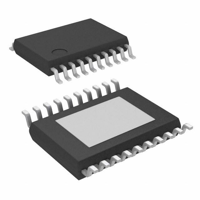


 工商网监
湘ICP备2023018690号
工商网监
湘ICP备2023018690号
