User's Guide
SNAA052A – February 2008 – Revised May 2013
AN-1768 LME49600 Headphone Amplifier
Evaluation Board
1
Quick Start Guide
1. Apply a ±2.5V to ±17V power supply’s voltage to the respective “V+”, “GND” and “V–” pins on JU19.
2. Apply a stereo audio signal to the RCA jacks J1 (Right) and J2 (Left) or jumpers JU1 (Right) and JU17
(Left), observing the signal input pin and the ground (GND) pin. Though not typically installed, a stereo
signal can also be applied to headphone jack HPJ1.
3. Connect a load to JU14 (Left) and another load to JU15 (Right), observing the signal output pin and
the ground (GND) pin. The stereo signal output is also available on the 1/8” stereo headphone jack
located in the board's “OUTPUT” section.
4. Use VR1 to control the output signal amplitude.
5. Apply power. Make measurements. Plug in a pair of headphones. Enjoy.
2
Introduction
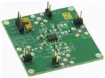
To help the user investigate and evaluate the LME49600's performance and capabilities, a fully populated
demonstration board was created. Please click here for availability. This board is shown in Figure 1.
Connected to an external power supply (±2.5V to ±17V) and a signal source. The LME49600
demonstration board easily demonstrates the amplifier's features.
All trademarks are the property of their respective owners.
SNAA052A – February 2008 – Revised May 2013
Submit Documentation Feedback
AN-1768 LME49600 Headphone Amplifier Evaluation Board
Copyright © 2008–2013, Texas Instruments Incorporated
1
�General Description
www.ti.com
Figure 1. LME49600/LME49720 Stereo Headphone Amplifier Demonstration Board
3
General Description
The LME49600 is a high performance, low distortion high fidelity 250mA audio buffer. Whereas there are
many uses for the LME49600, this application report describes a headphone amplifier circuit and
associated demonstration board. Designed for use inside an operational amplifier’s feedback loop, it
increases output current, improves capacitive load drive, and eliminates thermal feedback.
The LME49600 offers a pin-selectable bandwidth: a low current, 110MHz bandwidth mode that consumes
8mA and a wide 180MHz bandwidth mode that consumes 15mA. In both modes the LME49600 has a
nominal 2000V/μs slew rate. Bandwidth is easily adjusted by either leaving the BW pin unconnected,
connecting a resistor between the BW pin and the VEE pin or connecting the BW pin directly to the VEE pin.
The LME49600 is fully protected through internal current limit and thermal shutdown.
4
Operating Conditions
–40°C ≤ TA ≤ 85°C
Temperature Range
Amplifier Power
Supply Voltage
2
2.5V ≤ VS ±17V
AN-1768 LME49600 Headphone Amplifier Evaluation Board
SNAA052A – February 2008 – Revised May 2013
Submit Documentation Feedback
Copyright © 2008–2013, Texas Instruments Incorporated
�Board Features
www.ti.com
5
Board Features
The LME49600/LME49720 Stereo Headphone Amplifier demonstration board has all of the necessary
connections, using RCA jacks, 1/8” stereo headphone jack and 0.100” headers, to apply the power supply
voltage and the audio input signals. The amplified audio signal is available on both a stereo headphone
jack and auxiliary output connections.
Also present on the demonstration board is a potentiometer to control the stereo output signal magnitude.
6
Schematic
Figure 2 shows the LME49600/LME49720 Stereo Headphone Amplifier Demonstration Board schematic.
Table 1 is a list of the connections and their functions.
V+
V+
C19
0.1 PF
C24
C1
+
6
1
3
VR1-A
2
2
8
+
U1-A
U3
BW
4
LME49600
3
C23
+
JU1
1
C2
4
4.7 PF
+
See note
R3
1k
1.0 PF
V-
4.7 PF
C20
C5
HPJ1
R9
1M
3
5
4
2
1
R10
V-
1.0 PF
6
5
U1-B
See note
7
+
1M
C6
2
0.1 PF
JU15
R5
1k
V+
JU6
C21
JU14
HPJ2
3
5
4
2
1
0.1 PF
C10
1.0 PF
+
J2 1
JU17
V+
5
4
3
VR1-B
1
U2-A
-
U4
BW
See note
22 PF
LME49600
1
C9
4.7 PF
C22
R4
1k
1.0 PF
V-
4
3
C4
4
R2
1k
1
1.0 PF
V+
4.7 PF
C12
+
S1-A
+
2
3
8
+
5
2
C3
+
J1 1
5
2
1
-
R1
1k
2
1.0 PF
V-
3
1
5
4
3
1
See note
U2-B
+
C8
7
6
R6
1k
VBAT2
4
C14
+
1M
S1-B
JU4
R12
-
JU19
2
5
1.0 PF
6
V+
BAT1
4
0.1 PF
C7
R11
1M
1
2
22 PF
V-
1.0 PF
Figure 2. LME49600 Demonstration Board Schematic
Note: The LM4562, LME49720, or LME49860 can be used.
SNAA052A – February 2008 – Revised May 2013
Submit Documentation Feedback
AN-1768 LME49600 Headphone Amplifier Evaluation Board
Copyright © 2008–2013, Texas Instruments Incorporated
3
�Connections
7
www.ti.com
Connections
Connecting to the world is accomplished through a combination of RCA jacks, 1/8” stereo headphone
jacks and 0.100” headers on the LME49600 demonstration board. The functions of the different headers,
1/8” headphone jacks and RCA jacks are detailed in Table 1.
Table 1. LME49600 Demonstration Board Connections
Designator
JU17
J2
HPJ1
J1
This is an RCA connector that parallels the pins on JU17.
Stereo, 1/8” headphone jack. Used for stereo signal input. Left channel input is on the tip connector and
the right channel input is on the ring connector. Ground is on the sleeve connector.
This is an RCA connector that parallels the pins on JU1.
JU1
This is the connection to the amplifier’s right channel input. Apply an external signal source’s positive
voltage to the JU1 pin labeled “RT IN” and the signal source’s ground signal to the pin labeled “GND.”
JU19
Power supply connection. Connect an external split power supply’s voltage source ±2.5V to ±17V to the
JU19 pin labeled (“V+” and “V-”)” and the supply’s ground source to the pin labeled “GND.”
JU14
This is the connection to the amplifier’s single-ended, ground-referenced left channel output. Connect
the JU14 pin labeled “LT OUT” and the pin labeled “GND” to the positive and ground inputs,
respectively, of an external signal measurement device. JU14’s pin labeled “LT OUT” corresponds to the
headphone jack’s “tip” connection. J5’s pin labeled “GND“ corresponds to the headphone jack’s “sleeve”
(or ground) connection.
HPJ2
Stereo, 1/8” headphone jack. Used for stereo signal output. Left channel output is on the tip connector
and the right channel output is on the ring connector. Ground is on the sleeve connector.
JU15
This is the connection to the amplifier’s ground-referenced right channel output. Connect the JU15 pin
labeled “RT OUT” and the pin labeled “GND” to the positive and ground inputs, respectively, of an
external signal measurement device. JU15’s pin labeled “RT OUT” corresponds to the headphone jack’s
“ring” connection. J4’s pin labeled “GND“ corresponds to the headphone jack’s “sleeve” (or ground)
connection.
JU4, JU6
8
Function or Use
This is the connection to the amplifier’s left channel input. Apply an external signal source’s positive
voltage to the JU17 pin labeled “LT IN” and the signal source’s ground signal to the pin labeled “GND.”
These connections allow monitoring the left and right channel DC servo outputs, respectively.
PCB Layout Guidelines
This section provides general practical guidelines for PCB layouts that use various power and ground
traces. Designers should note that these are only "rule-of-thumb" recommendations and the actual results
are predicated on the final layout.
8.1
Power and Ground Circuits
Star trace routing techniques can have a major positive impact on low-level signal performance. Star trace
routing refers to using individual traces that radiate from a signal point to feed power and ground to each
circuit or even device.
4
AN-1768 LME49600 Headphone Amplifier Evaluation Board
SNAA052A – February 2008 – Revised May 2013
Submit Documentation Feedback
Copyright © 2008–2013, Texas Instruments Incorporated
�Bill of Materials
www.ti.com
9
Bill of Materials
RefDes
Part Description
Tolerance
Rating
Package
Type
Manufacturer
and Part Number
BAT1– BAT2
9V Battery Terminal (male &
female) [Not Installed]
C1 – C8
MULITYLAYER CERAMIC
CAPACITOR
1.0μF
±20%
25V
805
TDK
C2012X5R1E105M
C9 C10, C23 –
C24
TANTALUM ELECTROLYTIC
CAPACITOR
4.7μF
±10%
35V
B CASE
AVX
TPSB475K035R0700
22μF
±20%
25V
C CASE
AVX
TPSD226M025#011
0.1μF
±10%
25V
603
1/4W resistor
1kΩ
±1%
1/4W
1/4W resistor
1MΩ
±1%
1/4W
S1
SWITCH SLIDE DPDT
[Not Installed]
DPDT
U1, U2
LME49720 (Can also use
LM4562, LME49860)
Texas Instruments
LME49720
(LM4562 or LME49860)
U3, U4
LME49600
Texas Instruments
LME49600
VR1
Dual gauged potentiometer
C12, C14
C19 – C22
CERAMIC CAPACITOR
HPJ1– HPJ2
1/8” Stereo Headphone Jack
J1 – J2
RCA jack
JU1, JU4, JU6,
JU14, JU15, JU17
100mil pin pitch, two pin
JU19
100mil pin pitch, three pin
R1 – R6
R9 – R12
10
Value
KEYSTONE
593 (Female) & 594 (Male)
TDK
C1608X7R1E104K
1/4W, Axial
YAGEO
MFR-25FBF-1K00
1/4W, Axial
YAGEO
MFR-25FBF-1M00
PANASONIC
EVJ-Y00F30A14
10kΩ
Demonstration Board PCB Layout
Figure 3 through Figure 6 show the different layers used to create the LME49600 demonstration board.
Figure 3 is the silkscreen that shows parts location, Figure 4 is the top layer, Figure 5 is the bottom layer,
and Figure 6 is the bottom silkscreen layer.
SNAA052A – February 2008 – Revised May 2013
Submit Documentation Feedback
AN-1768 LME49600 Headphone Amplifier Evaluation Board
Copyright © 2008–2013, Texas Instruments Incorporated
5
�Demonstration Board PCB Layout
www.ti.com
Figure 3. Top Silkscreen
Figure 4. Top Layer
6
AN-1768 LME49600 Headphone Amplifier Evaluation Board
SNAA052A – February 2008 – Revised May 2013
Submit Documentation Feedback
Copyright © 2008–2013, Texas Instruments Incorporated
�Demonstration Board PCB Layout
www.ti.com
Figure 5. Bottom Layer
Figure 6. Bottom Silk Layer
SNAA052A – February 2008 – Revised May 2013
Submit Documentation Feedback
AN-1768 LME49600 Headphone Amplifier Evaluation Board
Copyright © 2008–2013, Texas Instruments Incorporated
7
�Typical Performance
11
www.ti.com
Typical Performance
0.01
0.01
THD+N (%)
0.001
1
0.1
0.01
0.001
OUTPUT POWER (W)
OUTPUT POWER (W)
Figure 7. THD+N vs Output Power
LME49720/LME49600 headphone amplifier
into (from top to bottom at 0.1mW):
16Ω, 32Ω, 64Ω, 300Ω
(VS = ±3V, f = 100Hz, 22Hz ≤ BW ≤ 22kHz)
0.0001
0.000001
1
0.1
0.01
0.001
0.0001
0.00001
0.00001
0.0001
0.00001
0.0001
0.000001
THD+N (%)
0.001
Figure 8. THD+N vs Output Power
LME49720/LME49600 headphone amplifier
into (from top to bottom at 10mW):
16Ω, 32Ω, 64Ω, 300Ω
(VS = ±9V, f = 100Hz, 22Hz ≤ BW ≤ 22kHz)
0.01
0.01
OUTPUT POWER (W)
Figure 9. THD+N vs Output Power
LME49720/LME49600 headphone amplifier
into (from top to bottom at 10mW):
16Ω, 32Ω, 64Ω, 300Ω
(VS = ±15V, f = 100Hz, 22Hz ≤ BW ≤ 22kHz)
8
AN-1768 LME49600 Headphone Amplifier Evaluation Board
1
0.1
0.01
0.001
0.0001
0.0001
0.00001
10
1
0.1
0.01
0.001
0.0001
0.000001
0.00001
0.00001
0.0001
0.001
0.000001
THD+N (%)
THD+N (%)
0.001
OUTPUT POWER (W)
Figure 10. THD+N vs Output Power
LME49720/LME49600 headphone amplifier
into (from top to bottom at 0.1mW):
16Ω, 32Ω, 64Ω, 300Ω
(VS = ±3V, f = 1kHz, 400Hz ≤ BW ≤ 22kHz)
SNAA052A – February 2008 – Revised May 2013
Submit Documentation Feedback
Copyright © 2008–2013, Texas Instruments Incorporated
�Typical Performance
www.ti.com
0.01
0.001
0.001
OUTPUT POWER (W)
Figure 11. THD+N vs Output Power
LME49720/LME49600 headphone amplifier
into (from top to bottom at 10mW):
16Ω, 32Ω, 64Ω, 300Ω
(VS = ±9V, f = 1kHz, 400Hz ≤ BW ≤ 22kHz)
10
1
0.1
0.01
0.001
0.0001
1
0.01
0.001
0.00001
0.000001
0.00001
0.1
0.00001
0.0001
0.0001
0.000001
0.0001
0.00001
THD+N (%)
THD+N (%)
0.01
OUTPUT POWER (W)
Figure 12. THD+N vs Output Power
LME49720/LME49600 headphone amplifier
into (from top to bottom at 10mW):
16Ω, 32Ω, 64Ω, 300Ω
(VS = ±15V, f = 1kHz, 400Hz ≤ BW ≤ 22kHz)
0.01
0.01
THD+N (%)
THD+N (%)
0.001
0.001
OUTPUT POWER (W)
Figure 13. THD+N vs Output Power
LME49720/LME49600 headphone amplifier
into (from top to bottom at 0.1mW):
16Ω, 32Ω, 64Ω, 300Ω
(VS = ±3V, f = 10kHz, 400Hz ≤ BW ≤ 80kHz)
1
0.1
0.01
0.001
0.00001
0.000001
1
0.1
0.01
0.001
0.00001
0.0001
0.00001
0.000001
0.0001
0.0001
0.0001
OUTPUT POWER (W)
Figure 14. THD+N vs Output Power
LME49720/LME49600 headphone amplifier
into (from top to bottom at 20mW):
16Ω, 32Ω, 64Ω, 300Ω
(VS = ±9V, f = 10kHz, 400Hz ≤ BW ≤ 80kHz)
0.01
0.001
THD+N (%)
THD+N (%)
0.001
10
1
0.1
0.01
0.001
0.0001
0.000001
0.00001
0.00001
0.0001
0.0001
10
100
1k
10k
100k
FREQUENCY (Hz)
OUTPUT POWER (W)
Figure 15. THD+N vs Output Power
LME49720/LME49600 headphone amplifier
into (from top to bottom at 20mW):
16Ω, 32Ω, 64Ω, 300Ω
(VS = ±15V, f = 10kHz, 400Hz ≤ BW ≤ 80kHz)
SNAA052A – February 2008 – Revised May 2013
Submit Documentation Feedback
Figure 16. THD+N vs Frequency
LME49720/LME49600 headphone amplifier
into (from top to bottom at 5kHz): 16Ω at 3mW, 32Ω at
3mW, 300Ω at 0.3mW, and 64Ω at 1.5mW
(VS = ±3V, < 10Hz ≤ BW ≤ 80kHz)
AN-1768 LME49600 Headphone Amplifier Evaluation Board
Copyright © 2008–2013, Texas Instruments Incorporated
9
�Revision History
0.01
0.001
0.001
THD+N (%)
THD+N (%)
www.ti.com
0.01
0.0001
0.0001
0.00001
10
100
1k
10k
0.00001
10
100k
FREQUENCY (Hz)
100
1k
10k
100k
FREQUENCY (Hz)
Figure 17. THD+N vs Frequency
Figure 18. THD+N vs Frequency
LME49720/LME49600 headphone amplifier
LME49720/LME49600 headphone amplifier
into (from top to bottom at 5kHz): 16Ω at 100mW, 32Ω into (from top to bottom at 5kHz): 16Ω at 100mW, 32Ω
at 100mW, 64Ω at 35mW, and 300Ω at 8mW
at 100mW, 64Ω at 150mW, and 300Ω at 30mW
(VS = ±9V, < 10Hz ≤ BW ≤ 80kHz)
(VS = ±15V, < 10Hz ≤ BW ≤ 80kHz)
12
10
Revision History
Rev
Date
1.0
02/29/08
Description
Initial release.
AN-1768 LME49600 Headphone Amplifier Evaluation Board
SNAA052A – February 2008 – Revised May 2013
Submit Documentation Feedback
Copyright © 2008–2013, Texas Instruments Incorporated
�IMPORTANT NOTICE
Texas Instruments Incorporated and its subsidiaries (TI) reserve the right to make corrections, enhancements, improvements and other
changes to its semiconductor products and services per JESD46, latest issue, and to discontinue any product or service per JESD48, latest
issue. Buyers should obtain the latest relevant information before placing orders and should verify that such information is current and
complete. All semiconductor products (also referred to herein as “components”) are sold subject to TI’s terms and conditions of sale
supplied at the time of order acknowledgment.
TI warrants performance of its components to the specifications applicable at the time of sale, in accordance with the warranty in TI’s terms
and conditions of sale of semiconductor products. Testing and other quality control techniques are used to the extent TI deems necessary
to support this warranty. Except where mandated by applicable law, testing of all parameters of each component is not necessarily
performed.
TI assumes no liability for applications assistance or the design of Buyers’ products. Buyers are responsible for their products and
applications using TI components. To minimize the risks associated with Buyers’ products and applications, Buyers should provide
adequate design and operating safeguards.
TI does not warrant or represent that any license, either express or implied, is granted under any patent right, copyright, mask work right, or
other intellectual property right relating to any combination, machine, or process in which TI components or services are used. Information
published by TI regarding third-party products or services does not constitute a license to use such products or services or a warranty or
endorsement thereof. Use of such information may require a license from a third party under the patents or other intellectual property of the
third party, or a license from TI under the patents or other intellectual property of TI.
Reproduction of significant portions of TI information in TI data books or data sheets is permissible only if reproduction is without alteration
and is accompanied by all associated warranties, conditions, limitations, and notices. TI is not responsible or liable for such altered
documentation. Information of third parties may be subject to additional restrictions.
Resale of TI components or services with statements different from or beyond the parameters stated by TI for that component or service
voids all express and any implied warranties for the associated TI component or service and is an unfair and deceptive business practice.
TI is not responsible or liable for any such statements.
Buyer acknowledges and agrees that it is solely responsible for compliance with all legal, regulatory and safety-related requirements
concerning its products, and any use of TI components in its applications, notwithstanding any applications-related information or support
that may be provided by TI. Buyer represents and agrees that it has all the necessary expertise to create and implement safeguards which
anticipate dangerous consequences of failures, monitor failures and their consequences, lessen the likelihood of failures that might cause
harm and take appropriate remedial actions. Buyer will fully indemnify TI and its representatives against any damages arising out of the use
of any TI components in safety-critical applications.
In some cases, TI components may be promoted specifically to facilitate safety-related applications. With such components, TI’s goal is to
help enable customers to design and create their own end-product solutions that meet applicable functional safety standards and
requirements. Nonetheless, such components are subject to these terms.
No TI components are authorized for use in FDA Class III (or similar life-critical medical equipment) unless authorized officers of the parties
have executed a special agreement specifically governing such use.
Only those TI components which TI has specifically designated as military grade or “enhanced plastic” are designed and intended for use in
military/aerospace applications or environments. Buyer acknowledges and agrees that any military or aerospace use of TI components
which have not been so designated is solely at the Buyer's risk, and that Buyer is solely responsible for compliance with all legal and
regulatory requirements in connection with such use.
TI has specifically designated certain components as meeting ISO/TS16949 requirements, mainly for automotive use. In any case of use of
non-designated products, TI will not be responsible for any failure to meet ISO/TS16949.
Products
Applications
Audio
www.ti.com/audio
Automotive and Transportation
www.ti.com/automotive
Amplifiers
amplifier.ti.com
Communications and Telecom
www.ti.com/communications
Data Converters
dataconverter.ti.com
Computers and Peripherals
www.ti.com/computers
DLP® Products
www.dlp.com
Consumer Electronics
www.ti.com/consumer-apps
DSP
dsp.ti.com
Energy and Lighting
www.ti.com/energy
Clocks and Timers
www.ti.com/clocks
Industrial
www.ti.com/industrial
Interface
interface.ti.com
Medical
www.ti.com/medical
Logic
logic.ti.com
Security
www.ti.com/security
Power Mgmt
power.ti.com
Space, Avionics and Defense
www.ti.com/space-avionics-defense
Microcontrollers
microcontroller.ti.com
Video and Imaging
www.ti.com/video
RFID
www.ti-rfid.com
OMAP Applications Processors
www.ti.com/omap
TI E2E Community
e2e.ti.com
Wireless Connectivity
www.ti.com/wirelessconnectivity
Mailing Address: Texas Instruments, Post Office Box 655303, Dallas, Texas 75265
Copyright © 2013, Texas Instruments Incorporated
�