User's Guide
SNVA231B – January 2008 – Revised April 2013
AN-1610 LP5552 Evaluation Board
1
LP5552 Overview
The LP5552 is a PWI™ 2.0 compliant Energy Management Unit for reducing power consumption of standalone mobile phone processors such as baseband or applications processors.
The LP5552 contains two advanced, digitally controlled switching regulators for supplying variable voltage
to processor core and memory. The device also integrates 5 programmable LDO regulators for powering
I/O and PLLs, as well as maintaining memory retention in sleep-mode.
The device is controlled via the PWI 2.0 open-standard interface. The LP5552 operates cooperatively with
PowerWise™ technology-compatible processors to optimize supply voltages adaptively over process and
temperature variations or dynamically using frequency/voltage pre-characterized look-up tables.
2
Evaluation Board Overview
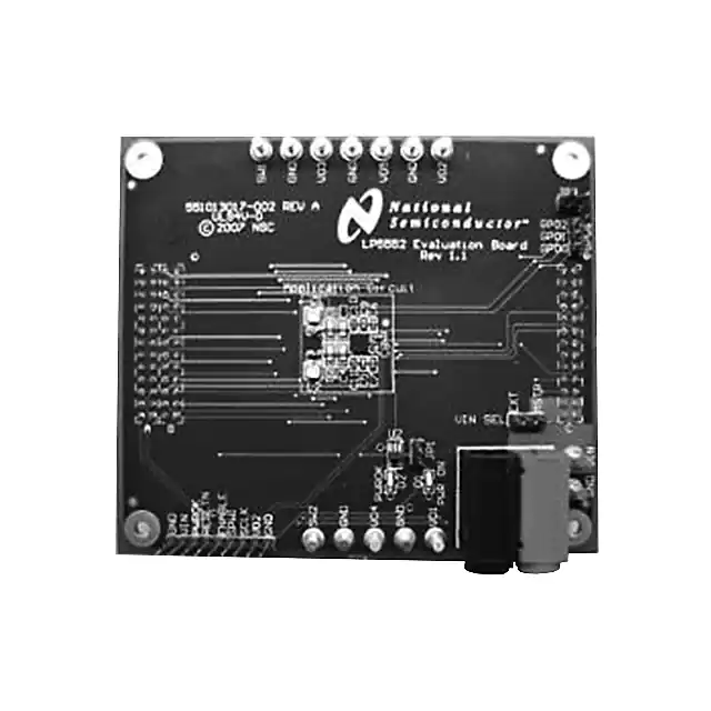
The LP5552 Evaluation Board, Figure 1, can be operated standalone or from a mainboard such as the
PowerWise Evaluation Kit (PEK) or USB2PWI interface board.
The evaluation board ships with the USB2PWI interface board and a graphical user interface (GUI) to
easily control the features of the LP5552 from a PC. For information on the GUI, see AN-1653 User's
Graphical User Interface (GUI) for LP555x Evaluation Board PowerWise Technology Compliant Energy
Management Unit Application Report (SNVA251).
The LP5552 is configured to operate with the following conditions:
Parameter
Default Voltage
Voltage Range
VIN
3.6V
2.7 - 4.8V
IOUT
VCORE1
1.235V
0.6 - 1.235V
800mA
VCORE2
1.235V
0.6 - 1.235V
800mA
VO1
1.2V
0.7 - 2.2V
100mA
VO2
3.3V
1.5 - 3.3V
250mA
VO3
1.25V
0.6 - 1.35V
50mA (High IQ)
VO4
1.25V
0.6 - 1.35V
50mA (High IQ)
VO5
3.3V
1.2 - 3.3V
250mA
Note that all the regulators can be programmed to different output voltages once the part is active.
The LP5552 can be powered externally (bench supply), or from the PEK or USB2PWI interface board
(depending on the mainboard being used). Jumper "VIN SEL" must be set to the appropriate power
source.
Jumper
Purpose
Note
VIN SEL
Input voltage selection
MSTR: LP5552 powered from attached mainboard; DEFAULT
EXT: LP5552 powered from external supply
PWI, PowerWise are trademarks of Texas Instruments.
All other trademarks are the property of their respective owners.
SNVA231B – January 2008 – Revised April 2013
Submit Documentation Feedback
Copyright © 2008–2013, Texas Instruments Incorporated
AN-1610 LP5552 Evaluation Board
1
�Evaluation Board Overview
www.ti.com
There are two additional jumpers on the LP5552 evaluation board. They behave as follows.
Jumper
Purpose
Note
JP1
Disconnect indicator
LEDs and PWROK buffer
ON: The PWR ON and PWROK indicators are active; DEFAULT
JP2
Disconnect GPO pull-up
resistors
ON: The 10K pull-up resistors are connected to the GPO pins; DEFAULT
OFF: The buffer and LEDs will remain unpowered
OFF: The GPO pull-up resistors are disconnected, for use with CMOS outputs
Figure 1. LP5552 Evaluation Board
2
AN-1610 LP5552 Evaluation Board
SNVA231B – January 2008 – Revised April 2013
Submit Documentation Feedback
Copyright © 2008–2013, Texas Instruments Incorporated
�Connecting the LP5552 to the USB2PWI Interface Board
www.ti.com
3
Connecting the LP5552 to the USB2PWI Interface Board
The LP5552 evaluation board can be connected to the USB2PWI interface board for convenient control of
the PWI and all the LP5552 functions via a simple register-based GUI. Figure 2 shows the USB2PWI
interface board. See AN-1653 for instructions on how to use the GUI.
Figure 2. USB2PWI Interface Board
4
Connecting the LP5552 Evaluation Board to an External Controller
All signals related to the PWI signalling environment are available on a 1x9 header on the edge of the
board. Although primarily intended for signal inspection, this header also allows for external control of the
PWI, used to communicate with the LP5552. The pins are spaced at 100-mil intervals. The pin list of this
header is shown in Table 1. Input and output direction is with reference to the LP5552. VIN and VO2 are
provided as reference voltages to determine the drive levels for the signals RESETN, ENABLE, PWROK,
SPWI, and SCLK. The external controller should drive ENABLE and RESETN between VIN and GND,
while SPWI and SCLK should be driven between VO2 and GND. The PWROK output will have a logic-high
output at VIN.
Table 1. Pin Functions
Pin
Function
Type
Description
1
GND
GND
Ground
2
VIN
Output
VIN Sense
3
PWROK
Output
PWROK
4
RESETN
Input
VIN: Active
GND: LP5552 in reset
5
ENABLE
Input
VIN: On
GND: Disable LP5552
6
SPWI
Input/Output
PWI Data
7
SCLK
Input
PWI Clock
8
VO2
Output
VO2 Sense
9
GND
GND
Ground
SNVA231B – January 2008 – Revised April 2013
Submit Documentation Feedback
Copyright © 2008–2013, Texas Instruments Incorporated
AN-1610 LP5552 Evaluation Board
3
�Connecting the LP5552 Evaluation Board to the PEK
5
www.ti.com
Connecting the LP5552 Evaluation Board to the PEK
The PEK is designed to quickly and easily control the LP5552 for PowerWise Interface (PWI) compliance
testing. Figure 3 shows the PEK. See the PEK User’s Guide for more information.
Figure 3. PowerWise Evaluation Kit (PEK)
6
PCB Layout Considerations
The evaluation board is comprised of four layers. See Section 8 for layout artwork. From top to bottom
they are:
1. Top, component side
2. Ground plane
3. VIN plane
4. Bottom
Being a very high performance EMU in a small physical package requires that some care be taken when
placing the IC into the application circuit. The breakout of the IC should be done as similarly to the
example artwork as possible. Everything on the outer ring of the DSBGA should be routed on the
component layer while microvias are used to escape the remaining signals on the adjacent layer. The
layout should be done in the following order to ensure best performance:
1. Switchers
2. PowerWise Interface
3. Input Caps
4. LDO Output Caps
5. Any remaining layout
4
AN-1610 LP5552 Evaluation Board
SNVA231B – January 2008 – Revised April 2013
Submit Documentation Feedback
Copyright © 2008–2013, Texas Instruments Incorporated
�PCB Layout Considerations
www.ti.com
For good performance of the circuit, it is essential to place the input and output capacitors as close as
physically possible to the associated pin.
Sensitive components should be placed far from those components with high switching currents.
It is a good practice to minimize high-current and switching-current paths.
6.1
DC/DC Buck Switching Regulators
Due to the high switching currents and accuracy of the LP5552, this is the most crucial aspect of the
layout. And because the switchers are almost a complete mirror image of one another on the part, the
design is most easily placed symmetrically about the part.
The 10µF input capacitors should be placed first, as near to PVDDx and PGNDx as possible. PVDDx
(pins A6 and A1) are the voltage rails for the high-side power FETs. PGNDx (pins A4 and A3) are the
return paths for the low-side power FETs. As seen with C3 and C4 in the artwork, these components have
their associated pads very near the pins that they will decouple. These capacitors are important in
sourcing charge during switching events.
The 10µF output capacitors are the next components to be placed. They can be seen in the artwork as C1
and C2. Best performance of the LP5552 will be realized by maintaining tight physical coupling of the
grounds of the input capacitor, output capacitor and PGND pin for each switcher. By placing the
input/output capacitors as depicted, a channel is created that will allow routing the switching node out to
the inductor between the pads of the input and output capacitors.
The output magnetics should be placed in a way that best allows the switching node, output node, and
supplied load to be routed easily. The inductors, and associated connections, are the least sensitive to
layout variation. Note that the evaluation board contains a 0-ohm series resistor between the switching
node and the inductor. This is included as a means to more easily make measurements on the evaluation
board and is NOT required in the application circuit.
Once placement of these components has been completed, the associated wiring/routing should be done.
The switching nodes should be routed to their associated inductors. Next, a ground polygon and/or plane
should be used to tie all capacitor grounds together and to the PGNDs. An example of this is shown in the
board artwork. Here we have a pour on the top layer that connects everything together, and we stitched it
into the ground plane to maintain the same potential at both points. There will be quite a bit of switching
current in this area so it should be physically isolated from other sensitive circuitry. Once the ground
connections are in place, proceed to routing the VIN connections. Finally, the FBx and RGND contacts
should be routed. The RGND should tie into a quiet location that will track the potential of the PGND pins.
On the evaluation board layout, this connection was made at the edge of the ground polygon on the top
layer. The FB lines should closely match the RGND routing to reduce the inductive loop of this pair. The
FB and RGND lines make up a high-side and low-side sense connection to maintain the accuracy of the
switcher outputs. The FB line should cross the switching trace as close to perpendicular as possible and
tie into the output node of the regulator. Low impedance power connections should be maintained for all of
these connections.
6.2
PowerWise Interface Routing
The PowerWise SCLK and SPWI lines should then be routed to the appropriate master in the system. If
this is a multi-master and/or multi-slave system, care should be taken in matching the trace lengths of all
segments of the PWI bus. Additionally, the designer must ensure that the electrical characteristics of the
interconnect do not violate the restrictions in the PowerWise Interface 2.0 specification.
6.3
Input Capacitors
Any additional input decoupling capacitors that are part of the design should now be placed and routed. In
the case of the evaluation board, this includes capacitors C5 and C6. They are general purpose caps and
are tied directly to the VIN plane on the board. It is not mandatory to include additional bypass caps,
however it is recommended. Low impedance connections are required to allow the capacitors to function
at their peak performance. Regardless of any decoupling capacitors, EVERY VIN CONNECTION SHOULD
HAVE ITS OWN ROUTING FROM THE SOURCE. Vias and/or traces should NOT be shared amongst VIN
pins. The PVDDx pins especially should have their own separate supply connections.
SNVA231B – January 2008 – Revised April 2013
Submit Documentation Feedback
Copyright © 2008–2013, Texas Instruments Incorporated
AN-1610 LP5552 Evaluation Board
5
�Bill of Materials
6.4
www.ti.com
LDO Output Capacitors
This step involves placing the output capacitors of the LDO regulators. If an LDO will not be used, it is not
necessary to place its output capacitor in the design. These capacitors should be placed as physically
close to the LP5552 IC as possible. Again, use low-impedance connections to the output capacitors for
best performance.
7
6
Bill of Materials
Item
Part Value
Part Number
Footprint
Description
Mfg.
A
2 × 13 Pin Array
9-146252-0-13
DIP-26
Mainboard Connector
AMP/Tyco
B
2 × 13 Pin Array
9-146252-0-13
DIP-26
Mainboard Connector
AMP/Tyco
C
2 × 13 Pin Array
9-146252-0-13
DIP-26
Mainboard Connector
AMP/Tyco
CA1
NL
0402
AVDD1 Bypass Cap
N/A
CA2
NL
0402
AVDD2 Bypass Cap
N/A
C1
10µF
LMK212BJ106KD
0805
SW1 Output Cap
Taiyo Yuden
C2
10µF
LMK212BJ106KD
0805
SW2 Output Cap
Taiyo Yuden
C3
10µF
LMK212BJ106KD
0805
SW1 Input Cap
Taiyo Yuden
C4
10µF
LMK212BJ106KD
0805
SW2 Input Cap
Taiyo Yuden
C5
0.1µF/16V/X5R/10%
0402
General Bypass Cap
N/A
C6
0.1µF/16V/X5R/10%
0402
General Bypass Cap
N/A
C7
2.2µF/10V/X5R/10%
0603
LDO1 Output Cap
N/A
C8
4.7µF/10V/X5R/10%
0603
LDO2 Output Cap
N/A
C9
4.7µF/10V/X5R/10%
0603
LDO5 Output Cap
N/A
C10
1.0µF/10V/X5R/10%
LMK105BJ105KV
0402
LDO3 Output Cap
Taiyo Yuden
C11
1.0µF/10V/X5R/10%
LMK105BJ105KV
0402
LDO4 Output Cap
Taiyo Yuden
C12
0.1µF/16V/X5R/10%
0402
PWROK Buffer Bypass
Cap
N/A
L1
1µH
LPS3010-102ML
LPS30xx
SW1 Output Inductor
Coilcraft
L2
1µH
LPS3010-102ML
LPS30xx
SW2 Output Inductor
Coilcraft
PWR ON
Red LED
LTST-C171KRKT
0805
Red Power On Indicator
Lite-On
PWROK
Green LED
LTST-C170KGKT
0805
Green PWROK Indicator
Lite-On
R1
NL
0603
Pull-up for ENABLE
N/A
R2
NL
0603
Pull-up for RESETN
N/A
R3
10K/0.1W/5%
CRCW060310K0JN
0603
SA1 Pull-down
Vishay/Dale
R4
10K/0.1W/5%
CRCW060310K0JN
0603
SA2 Pull-down
Vishay/Dale
R5
10K/0.1W/5%
CRCW060310K0JN
0603
SA3 Pull-down
Vishay/Dale
R6
10K/0.1W/5%
CRCW060310K0JN
0603
GPO0 Pull-up
Vishay/Dale
R7
10K/0.1W/5%
CRCW060310K0JN
0603
GPO1 Pull-up
Vishay/Dale
R8
10K/0.1W/5%
CRCW060310K0JN
0603
GPO2 Pull-up
Vishay/Dale
R9
1.5K/0.1W/5%
CRCW06031K50JN
0603
Mainboard Presence
Detect
Vishay/Dale
R10
1.5K/0.1W/5%
CRCW06031K50JN
0603
Mainboard Presence
Detect
Vishay/Dale
R11
240-ohm/0.1W/5%
CRCW0603240RJN
0603
Red LED Current Limit Res Vishay/Dale
R12
160-ohm/0.1W/5%
CRCW0603160RJN
0603
Green LED Current Limit
Res
Vishay/Dale
R13
0-ohm/0.063W/5%
0402
RGND Isolation Res
N/A
SW1_O
0-ohm/0.1W/5%
0603
Measurement Pads SW1
N/A
SW2_O
0-ohm/0.1W/5%
0603
Measurement Pads SW2
N/A
U1
LP5552 PMIC
LP5552
DSBGA-36 PowerWise PMIC
Texas Instruments
U2
Tri-State Buffer
NC7SZ126M5
SOT23-5
Fairchild Semi
AN-1610 LP5552 Evaluation Board
PWROK LED Buffer
SNVA231B – January 2008 – Revised April 2013
Submit Documentation Feedback
Copyright © 2008–2013, Texas Instruments Incorporated
�Layout Artwork
www.ti.com
8
Layout Artwork
Figure 4. Top Layer
Figure 5. L2, Ground Plane
SNVA231B – January 2008 – Revised April 2013
Submit Documentation Feedback
Copyright © 2008–2013, Texas Instruments Incorporated
AN-1610 LP5552 Evaluation Board
7
�Layout Artwork
www.ti.com
Figure 6. L3, VIN Plane
Figure 7. Bottom Layer
8
AN-1610 LP5552 Evaluation Board
SNVA231B – January 2008 – Revised April 2013
Submit Documentation Feedback
Copyright © 2008–2013, Texas Instruments Incorporated
�Layout Artwork
www.ti.com
Figure 8. Top Layer Close Up
Figure 9. L2 Close Up
SNVA231B – January 2008 – Revised April 2013
Submit Documentation Feedback
Copyright © 2008–2013, Texas Instruments Incorporated
AN-1610 LP5552 Evaluation Board
9
�Layout Artwork
www.ti.com
Figure 10. Bottom Layer Close Up
10
AN-1610 LP5552 Evaluation Board
SNVA231B – January 2008 – Revised April 2013
Submit Documentation Feedback
Copyright © 2008–2013, Texas Instruments Incorporated
�Evaluation Board Schematic
www.ti.com
9
Evaluation Board Schematic
Figure 11. LP5552 Evaluation Board Schematic
SNVA231B – January 2008 – Revised April 2013
Submit Documentation Feedback
AN-1610 LP5552 Evaluation Board
Copyright © 2008–2013, Texas Instruments Incorporated
11
�IMPORTANT NOTICE
Texas Instruments Incorporated and its subsidiaries (TI) reserve the right to make corrections, enhancements, improvements and other
changes to its semiconductor products and services per JESD46, latest issue, and to discontinue any product or service per JESD48, latest
issue. Buyers should obtain the latest relevant information before placing orders and should verify that such information is current and
complete. All semiconductor products (also referred to herein as “components”) are sold subject to TI’s terms and conditions of sale
supplied at the time of order acknowledgment.
TI warrants performance of its components to the specifications applicable at the time of sale, in accordance with the warranty in TI’s terms
and conditions of sale of semiconductor products. Testing and other quality control techniques are used to the extent TI deems necessary
to support this warranty. Except where mandated by applicable law, testing of all parameters of each component is not necessarily
performed.
TI assumes no liability for applications assistance or the design of Buyers’ products. Buyers are responsible for their products and
applications using TI components. To minimize the risks associated with Buyers’ products and applications, Buyers should provide
adequate design and operating safeguards.
TI does not warrant or represent that any license, either express or implied, is granted under any patent right, copyright, mask work right, or
other intellectual property right relating to any combination, machine, or process in which TI components or services are used. Information
published by TI regarding third-party products or services does not constitute a license to use such products or services or a warranty or
endorsement thereof. Use of such information may require a license from a third party under the patents or other intellectual property of the
third party, or a license from TI under the patents or other intellectual property of TI.
Reproduction of significant portions of TI information in TI data books or data sheets is permissible only if reproduction is without alteration
and is accompanied by all associated warranties, conditions, limitations, and notices. TI is not responsible or liable for such altered
documentation. Information of third parties may be subject to additional restrictions.
Resale of TI components or services with statements different from or beyond the parameters stated by TI for that component or service
voids all express and any implied warranties for the associated TI component or service and is an unfair and deceptive business practice.
TI is not responsible or liable for any such statements.
Buyer acknowledges and agrees that it is solely responsible for compliance with all legal, regulatory and safety-related requirements
concerning its products, and any use of TI components in its applications, notwithstanding any applications-related information or support
that may be provided by TI. Buyer represents and agrees that it has all the necessary expertise to create and implement safeguards which
anticipate dangerous consequences of failures, monitor failures and their consequences, lessen the likelihood of failures that might cause
harm and take appropriate remedial actions. Buyer will fully indemnify TI and its representatives against any damages arising out of the use
of any TI components in safety-critical applications.
In some cases, TI components may be promoted specifically to facilitate safety-related applications. With such components, TI’s goal is to
help enable customers to design and create their own end-product solutions that meet applicable functional safety standards and
requirements. Nonetheless, such components are subject to these terms.
No TI components are authorized for use in FDA Class III (or similar life-critical medical equipment) unless authorized officers of the parties
have executed a special agreement specifically governing such use.
Only those TI components which TI has specifically designated as military grade or “enhanced plastic” are designed and intended for use in
military/aerospace applications or environments. Buyer acknowledges and agrees that any military or aerospace use of TI components
which have not been so designated is solely at the Buyer's risk, and that Buyer is solely responsible for compliance with all legal and
regulatory requirements in connection with such use.
TI has specifically designated certain components as meeting ISO/TS16949 requirements, mainly for automotive use. In any case of use of
non-designated products, TI will not be responsible for any failure to meet ISO/TS16949.
Products
Applications
Audio
www.ti.com/audio
Automotive and Transportation
www.ti.com/automotive
Amplifiers
amplifier.ti.com
Communications and Telecom
www.ti.com/communications
Data Converters
dataconverter.ti.com
Computers and Peripherals
www.ti.com/computers
DLP® Products
www.dlp.com
Consumer Electronics
www.ti.com/consumer-apps
DSP
dsp.ti.com
Energy and Lighting
www.ti.com/energy
Clocks and Timers
www.ti.com/clocks
Industrial
www.ti.com/industrial
Interface
interface.ti.com
Medical
www.ti.com/medical
Logic
logic.ti.com
Security
www.ti.com/security
Power Mgmt
power.ti.com
Space, Avionics and Defense
www.ti.com/space-avionics-defense
Microcontrollers
microcontroller.ti.com
Video and Imaging
www.ti.com/video
RFID
www.ti-rfid.com
OMAP Applications Processors
www.ti.com/omap
TI E2E Community
e2e.ti.com
Wireless Connectivity
www.ti.com/wirelessconnectivity
Mailing Address: Texas Instruments, Post Office Box 655303, Dallas, Texas 75265
Copyright © 2013, Texas Instruments Incorporated
�