Using the LP8860-Q1EVM Evaluation Module
User's Guide
Literature Number: SNVU382A
April 2014 – Revised June 2014
�Contents
Preface ........................................................................................................................................ 5
1
Introduction ......................................................................................................................... 6
1.1
Trademarks ......................................................................................................................... 6
2
Description of the LP8860-Q1 ................................................................................................ 7
2.1
2.2
2.3
Features ....................................................................................................................... 7
Applications ................................................................................................................... 7
Typical Applications ......................................................................................................... 8
3
Hardware Setup.................................................................................................................. 12
4
Board Layout ..................................................................................................................... 13
5
Board Stackup ................................................................................................................... 15
6
Power Sequences ............................................................................................................... 16
6.1
6.2
Start-up Sequence ......................................................................................................... 16
Shutdown Sequence ....................................................................................................... 16
7
Evaluation Board Schematic ................................................................................................ 17
8
Bill of Materials .................................................................................................................. 19
9
Evaluation Software ............................................................................................................ 21
9.1
9.2
Setup .........................................................................................................................
Usage ........................................................................................................................
9.2.1 Pin Control Tab ....................................................................................................
9.2.2 Brightness Control Tab ...........................................................................................
9.2.3 Faults and Status Tab ............................................................................................
9.2.4 Boost Tab ..........................................................................................................
9.2.5 Fault and Adaptive Voltage Control Tab .......................................................................
9.2.6 LED Drivers Tab ...................................................................................................
9.2.7 Temperature Tab ..................................................................................................
9.2.8 EEPROM Map Tab................................................................................................
9.2.9 History Tab .........................................................................................................
21
21
23
24
25
26
27
28
31
32
33
A
Virtual COM Port Configuration ............................................................................................ 34
B
Virtual COM Port Communication ......................................................................................... 37
C
LED Load Board ................................................................................................................. 38
D
Quick Start Guide ............................................................................................................... 41
D.1
D.2
D.3
D.4
D.5
D.6
D.7
D.8
D.9
EVM Board Default Jumper and Cable Positions ......................................................................
First Step: Light up LEDs..................................................................................................
Changing EEPROM Parameters .........................................................................................
Recovering Original EEPROM Parameters .............................................................................
Changing Brightness Control from I2C/SPI Register Control to PWM Input Pin Control ..........................
Smooth Brightness Change with Slope Control ........................................................................
Changing Boost Switching Frequency to 2.2 MHz .....................................................................
Cluster Mode, 4 LED Strings with Independent Brightness Control .................................................
Using EVM without MCU (MSP430), Standalone Mode ..............................................................
41
46
48
49
51
52
53
55
57
Revision History .......................................................................................................................... 59
2
Contents
SNVU382A – April 2014 – Revised June 2014
Submit Documentation Feedback
Copyright © 2014, Texas Instruments Incorporated
�www.ti.com
List of Figures
2-1.
Typical Application, Simple PWM Control, VDD = 3.3 V, Charge Pump On, 4 Strings ............................ 8
2-2.
Typical Application, SPI Control, VDD = 5 V, Charge Pump Off, 2 Strings .......................................... 9
2-3.
Typical Application, I2C Control, VDD = 3.3 V, Charge Pump On, 4 Strings ....................................... 10
2-4.
Typical Application, without Serial Interface, VDD = 5 V, Charge Pump Off, 3 Strings ........................... 11
3-1.
...............................................................................
Top Layer ...................................................................................................................
Bottom Layer (GND) .......................................................................................................
PCB Layout Example ......................................................................................................
Evaluation Board Stackup .................................................................................................
Evaluation Board Schematic, Microcontroller and Related Components ...........................................
Evaluation Board Schematic, LP8860-Q1 and Main Components ..................................................
Main Window Structure ....................................................................................................
Main Window and Pin Control Tab.......................................................................................
Brightness Control Tab ....................................................................................................
Fault and Status Tab.......................................................................................................
Boost Controls Tab.........................................................................................................
Interactive Boost Diagram Window ......................................................................................
Fault and Adaptive Voltage Control Tab ................................................................................
LED Fault And Adaptive Voltage Control Functionality Diagram ....................................................
LED Driver Controls ........................................................................................................
LED Driver Diagram Window .............................................................................................
PLL Diagram Window......................................................................................................
PLL Calculator for External VSYNC (Steps Show Order for Applying Commands) ...............................
PLL Calculator for Internal Oscillator ....................................................................................
Temperature Sensors Control ............................................................................................
EEPROM Map ..............................................................................................................
History Tab ..................................................................................................................
Device Manager View. Select the Virtual COM Port ..................................................................
Open Properties by Clicking Right Mouse Button on Virtual COM Port ............................................
Select Port Settings from the Virtual COM Port Properties ...........................................................
Select Advanced from Virtual COM Port Properties and Select COM Port Number (9 or smaller) .............
LED Load Board - Top Side ..............................................................................................
LED Load Board - Bottom View ..........................................................................................
LED Load Board - Schematic Diagram..................................................................................
Forward Voltage for Cree Xlamp ML-B LEDs .........................................................................
Jumper Positions ...........................................................................................................
CPUMP Jumper ............................................................................................................
Interface Jumpers ..........................................................................................................
4-1.
4-2.
4-3.
5-1.
7-1.
7-2.
9-1.
9-2.
9-3.
9-4.
9-5.
9-6.
9-7.
9-8.
9-9.
9-10.
9-11.
9-12.
9-13.
9-14.
9-15.
9-16.
A-1.
A-2.
A-3.
A-4.
C-1.
C-2.
C-3.
C-4.
D-1.
D-2.
D-3.
Evaluation Board Connectors and Setup
SNVU382A – April 2014 – Revised June 2014
Submit Documentation Feedback
List of Figures
Copyright © 2014, Texas Instruments Incorporated
12
13
13
14
15
17
18
22
23
24
25
26
26
27
27
28
28
29
29
30
31
32
33
34
35
35
36
38
38
39
40
43
44
58
3
�www.ti.com
4
List of Figures
SNVU382A – April 2014 – Revised June 2014
Submit Documentation Feedback
Copyright © 2014, Texas Instruments Incorporated
�Preface
SNVU382A – April 2014 – Revised June 2014
Read This First
About this Manual
This user’s guide describes the module used to evaluate characteristics, operation, and use of the
LP8860-Q1 low EMI, high-performance 4-channel LED driver for automotive lighting. This document
includes a schematic diagram, PCB layout, and bill of materials (BOM). Evaluation software (SW) usage is
also described.
How to Use This Manual
This document contains the following chapters:
• Chapter 1: Introduction
• Chapter 2: Description of the LP8860-Q1
• Chapter 3: Hardware Setup
• Chapter 4: Board Layout
• Chapter 5: Board Stackup
• Chapter 6: Power Sequences
• Chapter 7: Evaluation Board Schematic
• Chapter 8: Bill of Materials
• Chapter 9: Evaluation Software
• Appendix A: Virtual COM Port Configuration
• Appendix B: Virtual COM Port Communication
• Appendix C: LED Load Board
• Appendix D: Quick Start Guide
Related Documentation from Texas Instruments
LP8860-Q1 data sheet
FCC Warning
This equipment is intended for use in a laboratory test environment only. It generates, uses, and can
radiate radio frequency energy and has not been tested for compliance with the limits of computing
devices pursuant to subpart J of part 15 of FCC rules, which are designed to provide reasonable
protection against radio frequency interference. Operation of this equipment in other environments may
cause interference with radio communications, in which case the user, at their own expense, will be
required to take whatever measures may be required to correct this interference.
If You Need Assistance
Contact your local TI sales representative.
SNVU382A – April 2014 – Revised June 2014
Submit Documentation Feedback
Read This First
Copyright © 2014, Texas Instruments Incorporated
5
�Chapter 1
SNVU382A – April 2014 – Revised June 2014
Introduction
The Texas Instruments LP8860-Q1EVM evaluation module (EVM) helps designers evaluate the operation
and performance of the LP8860-Q1 device. The LP8860-Q1EVM uses the LP8860-Q1 to drive up to 4
LED strings for LCD backlighting with high efficiency. Information about output voltage and current ratings
of the LP8860-Q1 can also be found in the device datasheet.
In order to facilitate ease of testing and evaluation of this circuit, the EVM contains a TI MSP430
microprocessor to provide easy communication via USB. Power supply connection for the VIN, VDD, and
test points for each signal can be found on the evaluation board. Windows® SW is used to control
I2C/SPI™ registers of the device. A separate LED board can be used as a load; it is also possible to
connect LCD panel to the output connectors.
For evaluation purposes, the EVM has been tested over a 3-V to 48-V input range. This voltage range is
within the recommended operating range for input voltage of the LP8860-Q1. Users are cautioned to
evaluate their specific operating conditions and choose components with the appropriate voltage ratings
before designing this support circuitry into a final product.
1.1
Trademarks
Windows is a registered trademark of Microsoft Corporation.
SPI is a trademark of Motorola.
All other trademarks are the property of their respective owners.
6
Introduction
SNVU382A – April 2014 – Revised June 2014
Submit Documentation Feedback
Copyright © 2014, Texas Instruments Incorporated
�Chapter 2
SNVU382A – April 2014 – Revised June 2014
Description of the LP8860-Q1
The LP8860-Q1 is an automotive high-efficiency LED driver with integrated boost controller. It has 4 highprecision current sinks that can be controlled by a PWM input signal, an SPI/I2C master, or both.
The boost converter has adaptive output voltage control based on the LED current sink headroom
voltages. This feature minimizes the power consumption by adjusting the voltage to the lowest sufficient
level in all conditions. A boost controller supports spread spectrum for switching frequency and an external
synchronization with a dedicated pin. The high switching frequency allows the LP8860-Q1 to avoid
disturbance for AM radio band.
The LP8860-Q1 supports built-in Hybrid PWM and Current Dimming which reduces EMI, extends the LED
lifetime, and increases the total optical efficiency. Phase-shift PWM allows reduced audible noise and
smaller boost output capacitors.
The LP8860-Q1 can drive an external p-FET to disconnect the input supply from the system in the event
of a fault and reduce inrush current and standby power consumption.
The input voltage range for LP8860-Q1 is 3 V to 48 V to support car stop/start conditions. The device
integrates extensive safety and protection features.
2.1
Features
•
•
•
•
•
•
•
•
•
•
2.2
Four High-Precision Current Sinks
– Current Matching 0.5% typ
– Output Current up to 150 mA/Channel
– Individual LED String Current Adjustment
– Dimming Ratio >13000:1 with External PWM Brightness Control
– 16-bit dimming control with SPI or I2C Control
– Two Modes: Display Mode and Cluster Mode with Individual Control
Hybrid PWM and Current Dimming for Higher LED Drive Optical Efficiency
Synchronization for LED PWM
Boost Controller With Programmable Switching Frequency 100 kHz to 2.2 MHz and Spread Spectrum
Option
Boost Synchronization Input
Input Voltage Operating Range 3 V to 48 V
Power Line FET Control for Inrush Current Protection and Standby Energy Saving
Automatic LED Current Reduction with External Temperature Sensor
Extensive Safety and Fault Tolerance Features
SPI or I2C Interface
Applications
•
Automotive Infotainment, Instrument Cluster and Backlighting Systems
SNVU382A – April 2014 – Revised June 2014
Submit Documentation Feedback
Description of the LP8860-Q1
Copyright © 2014, Texas Instruments Incorporated
7
�Typical Applications
2.3
www.ti.com
Typical Applications
VIN
3-40 V
D
RISENSE
L
CFLY
Q2
CIN
COUT
Q1
C1P
C1N
SD
VSENSE_N
GD
ISENSE
RSENSE
VSENSE_P
ISENSE_GND
VDD 3.3 V
VDD
CCPUMP
CVDD
CPUMP
FB
SQW
FILTER
UP TO 150 mA/STRING
LP8860-Q1
BOOST SYNC
OUT1
SYNC
V/H SYNC
OUT2
VSYNC
BRIGHTNESS
OUT3
PWM
OUT4
SCLK/SCL
MOSI/SDA
MISO
TSENSE
FAULT RESET
NSS
ENABLE
VDDIO/EN
NTC
ISET
VDDIO
RISET
IF
FAULT
FAULT
SGND
LGND
PAD
PGND
Figure 2-1. Typical Application, Simple PWM Control,
VDD = 3.3 V, Charge Pump On, 4 Strings
8
Description of the LP8860-Q1
SNVU382A – April 2014 – Revised June 2014
Submit Documentation Feedback
Copyright © 2014, Texas Instruments Incorporated
�Typical Applications
www.ti.com
VIN
3-40 V
D
RISENSE
L
Q2
CIN
COUT
Q1
C1P
C1N
SD
VSENSE_N
GD
ISENSE
RSENSE
VSENSE_P
ISENSE_GND
VDD 5 V
VDD
CCPUMP
CPUMP
FB
SQW
FILTER
UP TO 300 mA/STRING
LP8860-Q1
BOOST SYNC
OUT1
SYNC
V/H SYNC
OUT2
VSYNC
BRIGHTNESS
OUT3
PWM
SCLK
OUT4
SCLK/SCL
MOSI
MOSI/SDA
MISO
MISO
TSENSE
NSS
NSS
ENABLE
VDDIO/EN
NTC
ISET
VDDIO
RISET
IF
FAULT
FAULT
SGND
LGND
PAD
PGND
Figure 2-2. Typical Application, SPI Control,
VDD = 5 V, Charge Pump Off, 2 Strings
SNVU382A – April 2014 – Revised June 2014
Submit Documentation Feedback
Description of the LP8860-Q1
Copyright © 2014, Texas Instruments Incorporated
9
�Typical Applications
VIN
3-40 V
www.ti.com
D
RISENSE
L
CFLY
Q2
CIN
COUT
Q1
C1P
C1N
SD
VSENSE_N
GD
ISENSE
RSENSE
VSENSE_P
ISENSE_GND
VDD 3.3 V
VDD
CCPUMP
CVDD
CPUMP
FB
SQW
FILTER
UP TO 150 mA/STRING
LP8860-Q1
BOOST SYNC
V/H SYNC
BRIGHTNESS
SCL
SDA
OUT1
SYNC
OUT2
VSYNC
OUT3
PWM
OUT4
SCLK/SCL
MOSI/SDA
MISO
TSENSE
FAULT RESET
NSS
ENABLE
VDDIO/EN
NTC
ISET
VDDIO
RISET
IF
FAULT
FAULT
SGND
LGND
PAD
PGND
Figure 2-3. Typical Application, I2C Control,
VDD = 3.3 V, Charge Pump On, 4 Strings
10
Description of the LP8860-Q1
SNVU382A – April 2014 – Revised June 2014
Submit Documentation Feedback
Copyright © 2014, Texas Instruments Incorporated
�Typical Applications
www.ti.com
VIN
3-40 V
D
L
CIN
COUT
Q1
C1P
C1N
SD
VSENSE_N
GD
ISENSE
RSENSE
VSENSE_P
ISENSE_GND
VDD 5 V
VDD
CCPUMP
CPUMP
FB
SQW
FILTER
UP TO 150 mA/STRING
LP8860-Q1
OUT1
SYNC
OUT2
VSYNC
BRIGHTNESS
OUT3
PWM
OUT4
SCLK/SCL
MOSI/SDA
MISO
TSENSE
NSS
ENABLE
VDDIO/EN
ISET
IF
FAULT
SGND
LGND
PAD
PGND
Figure 2-4. Typical Application, without Serial Interface,
VDD = 5 V, Charge Pump Off, 3 Strings
SNVU382A – April 2014 – Revised June 2014
Submit Documentation Feedback
Description of the LP8860-Q1
Copyright © 2014, Texas Instruments Incorporated
11
�Chapter 3
SNVU382A – April 2014 – Revised June 2014
Hardware Setup
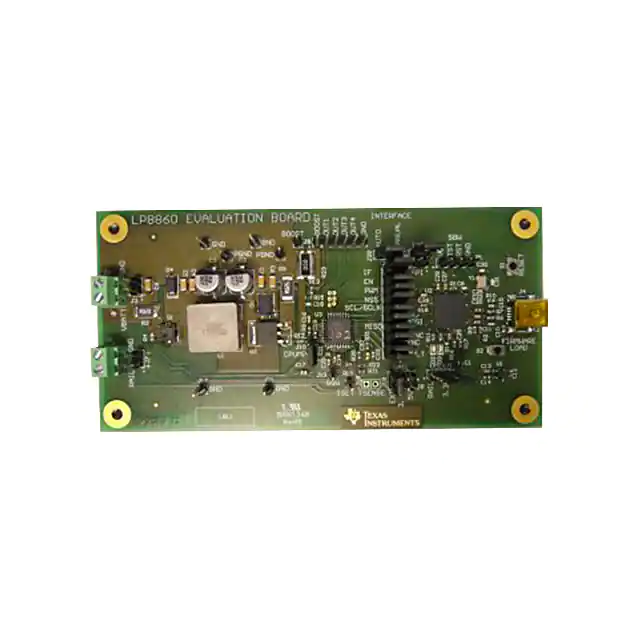
Figure 3-1 shows connectors and main components on the board.
Connectors for external
board or panel
Jumpers for connecting
C digital signals to
LP8860-Q1
Jumpers for
interface selection
Microcontroller and needed
external components for
I2C/SPI communication
USB
connector
VIN connector
3...40V
VDD connector
3...5V
LP8860-Q1 needed external
components
External NTC
connector
Rail (VDD) voltage selection
(USB 5V, 3.3V or external)
VDDIO voltage selection
(same as VDD or 3.3V)
USB ok, blinking
green LED
FAULT, red
LED
Kelvin connectors
Figure 3-1. Evaluation Board Connectors and Setup
Note. If charge pump is not in use, J10 “CPUMP” should be shorted.
12
Hardware Setup
SNVU382A – April 2014 – Revised June 2014
Submit Documentation Feedback
Copyright © 2014, Texas Instruments Incorporated
�Chapter 4
SNVU382A – April 2014 – Revised June 2014
Board Layout
Figure 4-1. Top Layer
Figure 4-2. Bottom Layer (GND)
SNVU382A – April 2014 – Revised June 2014
Submit Documentation Feedback
Board Layout
Copyright © 2014, Texas Instruments Incorporated
13
�www.ti.com
BATTERY
+VBATT -VBATT
R1
R2
Input capacitors
Q1
L1
Q1
C3
C4
C5
C4
D1
C8
1
R2
VDD
ISENSE_GND
CPUMP
FB
C2
SQW
4
C7
C6
MISO
17
NSS
TSENSE
VDDIO/EN
ISET
20
IF
11
FAULT
SGND
29
23
PAD
C1P
2
C1N
3
VDD
C1
7
VDD
24
OUT2
LGND 23
22
OUT3
SQW
4
21
OUT4
IF
8
VSENSE_N
5
20
VSENSE_P
6
19 VDDIO/EN
ISET
7
18
PWM
TSENSE
8
17
NSS
FILTER
9
10
PGND LGND
1
C5
OUT1 25
14
OUT4
21
16
MOSI/SDA
SCLK/SCL
22
15
24
FB 26
OUT3
15
OUT2
SCLK/SCL
14
PWM
16
MISO
18
ISENSE_GND 27
25
MOSI/SDA
OUT1
PGND 29
LP8860-Q1
SYNC
VSYNC
ISENSE 28
FILTER
13
19
C2
C7
Ground wire for
current sensor
R4
R3
13
12
R5
C6
26
12
9
27
Connection
between PGND
and GND
R5
Q2
SYNC
31
C1
ISENSE
R4
28
VSYNC
3
R3
GD 30
VDD 3.3V
GD
VSENSE_P
30
Feedback line
C9
Q2
C1N
CPUMP 31
6
C1P
SD
VSENSE_N
10 SGND
5
Output capacitors
C9
2
SD 32
32
C8
11
+VBATT
C3
D1
L1
FAULT
R1
VIA to GND plane
Figure 4-3. PCB Layout Example
See the LP8860-Q1 datasheet for PCB layout guidelines.
14
Board Layout
SNVU382A – April 2014 – Revised June 2014
Submit Documentation Feedback
Copyright © 2014, Texas Instruments Incorporated
�Chapter 5
SNVU382A – April 2014 – Revised June 2014
Board Stackup
Figure 5-1. Evaluation Board Stackup
Details:
• 2-layer board FR4
• Top layer - copper 35 µm
• Core 1.6 mm
• Bottom Layer - copper 35 µm
• Surface finish immersion gold
SNVU382A – April 2014 – Revised June 2014
Submit Documentation Feedback
Board Stackup
Copyright © 2014, Texas Instruments Incorporated
15
�Chapter 6
SNVU382A – April 2014 – Revised June 2014
Power Sequences
The LP8860-Q1 has a dual function VDDIO/EN pin. It acts as enable for the chip as well as
supply/reference voltage for IO logic. Device starts when VDD voltage is present and above the
VDD_UVLO voltage level and the VDDIO/EN voltage is set above threshold voltage (1.2 V).
6.1
Start-up Sequence
The backlight is started either by setting PWM input high or by writing not zero brightness value to
registers, depending on the brightness control mode and phase shift configuration. See the LP8860-Q1
datasheet for details.
6.2
Shutdown Sequence
The backlight is shut down either with setting PWM input low or by writing zero brightness value to
registers, depending on the brightness control mode and phase shift configuration. See the LP8860-Q1
datasheet for details.
16
Power Sequences
SNVU382A – April 2014 – Revised June 2014
Submit Documentation Feedback
Copyright © 2014, Texas Instruments Incorporated
�GND
RST
J5
47k
R1
SNVU382A – April 2014 – Revised June 2014
Submit Documentation Feedback
Copyright © 2014, Texas Instruments Incorporated
—)
—)
—)
C29
—)
C28
—)
C27
C26
—)
C25
—)
C22
C20
VCC
VCORE
V18
VUSB
VBUS
GND
2200pF
C8
SBW
1
S1
2
VCC
VBUS
VUSB
V18
VCORE
RST
TEST
XIN
XOUT
EN-UC
IF-UC
PWM-UC
FAULT-UC
GND
RESET
11
15
40
53
54
55
17
64
59
60
61
62
63
9
10
57
58
12
13
34
35
36
37
38
18
19
20
21
22
23
24
25
3
1
C12
—)
GND
GND
P5.0/A8/VEREF+
P5.1/A9/VEREFP5.2/XT2IN
P5.3/XT2OUT
P5.4/XIN
P5.5/XOUT
P3.0/UCB0SIMO/UCB0SDA
P3.1/UCB0SOMI/UCB0SCL
P3.2/UCB0CLK/UCA0STE
P3.3/UCA0TXD/UCA0SIMO
P3.4/UCA0RXD/UCA0SOMI
MSP430F5510IRGC
AVCC1
DVCC1
DVCC2
VBUS
VUSB
V18
VCORE
RST/NMI/SBWTDIO
TEST/SBWTCK
PJ.0/TDO
PJ.1/TDI/TCLK
PJ.2/TMS
PJ.3/TCK
OUT
GND
LP2985AIM5-3.3
3.3V
3.3V
VUSB
1
S2
2
QFN PAD
VSSU
AVSS1
AVSS2
DVSS1
DVSS2
PUR
PU.0/DP
PU.1/DM
P6.0/CB0/A0
P6.1/CB1/A1
P6.2/CB2/A2
P6.3/CB3/A3
P6.4/CB4/A4
P6.5/CB5/A5
P6.6/CB6/A6
P6.7/CB7/A7
P4.0/PM_UCB1STE/PM_UCA1CLK
P4.1/PM_UCB1SIMO/PM_UCB1SDA
P4.2/PM_UCB1SOMI/PM_UCB1SCL
P4.3/PM_UCB1CLK/PM_UCA1STE
P4.4/PM_UCA1TXD/PM_UCA1SIMO
P4.5/PM_UCA1RXD/PM_UCA1SOMI
P4.6/PM_NONE
P4.7/PM_NONE
65
49
14
56
16
39
51
50
52
1
2
3
4
5
6
7
8
41
42
43
44
45
46
47
48
26
27
28
29
30
31
32
33
GND
PUR
DP
DM
MISO-UC
SDA/MOSI-UC
SCL/SCLK-UC
NSS-UC
LED1
LED2
SYNC-UC
R7
GND
1
1
1
2
3
4
5
FAULT-UC
SCL/SCLK-UC
SDA/MOSI-UC
240
R14
240
R11
GND
C10
—)
GND
24MHz
2
2
C30
22pF
10k
R18
1.50k
R17
1.50k
R16
Orange
Green
D3
D2
GND
GND
1734035-2
J4
GND
ABM8-24.000MHZ-B2-T
Y1
2
1
G
4
3
G
LED2
LED1
27
C15
10pF
GND
VSYNC-UC
GND
R9
R10
1.50k 1.0Meg
27
R6
VBUS
VBUS
C11
10pF
GND
FIRMWARE LOADER
R2
PUR
100
PUR
DP
DM
P2.0/TA1.1
P2.1/TA1.2
P2.2/TA2CLK/SMCLK
P2.3/TA2.0
P2.4/TA2.1
P2.5/TA2.2
P2.6/RTCCLK/DMAE0
P2.7/UCB0STE/UCA0CLK
C14
—)
3.3V
3.3V
VCC
GND
—)
3.3V
VCC
C13
GND
4
5
C1
—)
1
2
3
ON/OFF
CBYP
GND
IN
U1
P1.0/TA0CLK/ACLK
P1.1/TA0.0
P1.2/TA0.1
P1.3/TA0.2
P1.4/TA0.3
P1.5/TA0.4
P1.6/TA1CLK/CBOUT
P1.7/TA1.0
U2
VBUS
RAIL
2
VCC
1
2
3
4
VCC
TEST
RST
VDDIO
C31
22pF
XIN
XOUT
VCC
J1
FAULT-UC
SYNC-UC
VSYNC-UC
MISO-UC
SDA/MOSI-UC
SCL/SCLK-UC
NSS-UC
PWM-UC
EN-UC
IF-UC
FAULT
SYNC
VSYNC
MISO
SDA/MOSI
SCL/SCLK
NSS
PWM
EN
IF
Chapter 7
SNVU382A – April 2014 – Revised June 2014
Evaluation Board Schematic
Figure 7-1. Evaluation Board Schematic, Microcontroller and Related Components
Evaluation Board Schematic
17
�Evaluation Board Schematic
Copyright © 2014, Texas Instruments Incorporated
VCC
FAULT
SYNC
VSYNC
MISO
SDA/MOSI
SCL/SCLK
NSS
PWM
EN
IF
RAIL
2
1
I2C
SPI
1727010
J6
RAIL
VCC
GND
GND
1
3
RAIL
1
2
J18
1
3
5
7
9
11
13
15
17
19
J11
VBUS
VBUS
3.3V
3.3V
EXTVDD
J7
2
4
2
4
6
1
2
3
J20
RAIL
GND
C17
—)
AUTO
MANUAL
FAULT
SYNC
VSYNC
MISO
SDA/MOSI
SCL/SCLK
NSS
PWM
EN
IFAUTO
J8
INTERFACE
2
4
6
8
10
12
14
16
18
20
1
3
5
USB
3.3V
EXT
1
2
J3
PGND
RAIL
PGND PGND
1727010
2
1
J10
PGND
GND
GND
—)
C19
0.02
—)
VSENSEN
VSENSEN
FAULT
IF
11
20
19
17
NSS
EN
14
MISO
SDA/MOSI 15
SCL/SCLK 16
18
13
VSYNC
PWM
12
SYNC
9
31
3
5
6
1
32
C24
—)
D4
VIN
LP8860QVFPRQ1
FAULT
IF
VDDIO/EN
NSS
MISO
MOSI/SDA
SCLK/SCL
PWM
VSYNC
SYNC
FILTER
CPUMP
VDD
VSENSE_N
VSENSE_P
SD
C1P
U3
C21
—)
ISENSE
GD
C1N
PGND
C5
—)
L1
SGND
LGND
PGND
EP
TSENSE
ISET
OUT4
OUT3
OUT2
OUT1
SQW
FB
10
23
29
8
7
21
22
24
25
4
26
27
28
30
2
PGND
GND
D1
R19
25.5k
1
R5
0.025
J13
3
C6
—)
J15
GND
GND
R22
15.0k
J19
OUT4
OUT3
OUT2
OUT1
GND
BOOST
BOOST
1
2
3
4
5
6
1
1
1
1
J22
J21
J17
J16
J14
J12
J9
HSYNC (20kHz & BW3db = 330Hz):
VCO[Mhz]
C33
C32
R21
5
10n
129n
14k
10
5n
65n
28k
20
2.5n
32n
56k
40
1.2n
16n
112k
HSYNC (50kHz & BW3db = 330Hz):
VCO[Mhz]
C33
C32
R21
5
22n
322n
5.6k
10
12n
161n 11,2k
20
6.2n
80n
22.3k
40
3.1n
40n
44,7k
VSYNC (50Hz & BW3db = 1Hz):
VCO[Mhz]
C33
C32
R21
5
100n
1.4u
85k
10
54n
0.7u 170k
20
27n
0.35u 338k
40
13.6n 0.175u 677k
GND
PGND
1
1
GND
BOOST
OUT1
OUT2
OUT3
OUT4
Filter components for different
Vsync and PLL frequences
2200pF
2200pF
C37
2200pF
C36
2200pF
C35
C34
C3
—)
J23
PGND
RT1
47.0k ohm
GND
1
2
R15
1.6Meg
R13
0
1
C7
—)
PGND
PGND
R20
3.00k
C18
47pF
PGND
PGND
1000pF
C16
R8
10
0
R23
Q2
IPD25N06S4L-30
PGND
ISENSE
2
1
SS5P10-M3/86A
PGND
GND
OUT4
OUT3
OUT2
OUT1
1
R12
10
1
SW
IHLP5050FDER220M5A
ISENSE_GND
C4
—)
PGND
C2
—)
PGND
PGND
B190-13-F
90V
VSENSEP
5
SD
20k
R4
GND
84.5k
—)
C33
R21
C23
—)
GND
VSENSEP
C32
C9
—)
SQJ461EP
3 Q1
2
1
4
SD
R3
4
3
J2
1
2
RAIL
IF
IFAUTO
BOOST
18
tƒ
VBATT
www.ti.com
Figure 7-2. Evaluation Board Schematic, LP8860-Q1 and Main Components
SNVU382A – April 2014 – Revised June 2014
Submit Documentation Feedback
�Chapter 8
SNVU382A – April 2014 – Revised June 2014
Bill of Materials
The following is the bill of materials for the LP8860-Q1EVM:
Description
Manufacturer
Part Number
Qty
C1, C10, C12, C14,
C19
Designator
CAP, CERM, 10uF, 16V, +/-20%,
X5R, 0603
Taiyo Yuden
EMK107BBJ106MA-T
5
C2, C3
CAP, AL, 33uF, 50V, +/-20%, 40
mohm, SMD
Panasonic
EEHZC1H330XP
2
C4, C5, C6, C7, C9
CAP, CERM, 10uF, 50V, +/-10%,
X5R, 1206_190
TDK
CGA5L3X5R1H106K160AB
5
CAP, CERM, 2200pF, 50V, +/-10%,
X7R, 0603
Kemet
C0603C222K5RACTU
1
CAP, CERM, 10pF, 50V, +/-5%,
C0G/NP0, 0603
AVX
06035A100JAT2A
2
C13
CAP, CERM, 0.01uF, 50V, +/-5%,
X7R, 0603
Kemet
C0603C103J5RACTU
1
C16
CAP, CERM, 1000pF, 100V, +/-10%,
X7R, 0603
AVX
06031C102KAT2A
1
C17
CAP, CERM, 10uF, 16V, +/-20%,
X5R, 0603
Taiyo Yuden
EMK107BBJ106MA-T
1
C18
CAP, CERM, 47pF, 50V, +/-5%,
C0G/NP0, 0603
Kemet
C0603C470J5GACTU
1
C20, C24, C27, C28,
C29
CAP, CERM, 0.1uF, 16V, +/-20%,
X7R, 0603
Kemet
C0603C104M4RACTU
5
C21, C22, C23, C26
CAP, CERM, 1uF, 10V, +/-10%, X5R,
0603
Kemet
C0603C105K8PACTU
4
CAP, CERM, 0.22uF, 16V, +/-10%,
X7R, 0603
Kemet
C0603C224K4RACTU
1
CAP, CERM, 22pF, 50V, +/-5%,
C0G/NP0, 0603
Kemet
C0603C220J5GACTU
2
C32
CAP, CERM, 1.2uF, 6.3V, +/-10%,
X5R, 0603
Kemet
C0603C125K9PACTU
1
C33
CAP, CERM, 0.1uF, 25V, +/-5%,
X7R, 0603
AVX
06033C104JAT2A
1
C34, C35, C36, C37
CAP, CERM, 2200pF, 50V, +/-10%,
X7R, 0603
Kemet
C0603C222K5RACTU
4
D1
Diode, Schottky, 100V, 5A, TO-277A
VishaySemiconductor
SS5P10-M3/86A
1
D2
LED, Green, SMD
Lite-On
LTST-C190GKT
1
D3
LED, Orange, SMD
Lite-On
LTST-C190KFKT
1
D4
Diode, Schottky, 90V, 1A, SMA
Diodes Inc.
B190-13-F
1
J1, J20
Header, TH, 100mil, 3x1, Gold
plated, 230 mil above insulator
Samtec
TSW-103-07-G-S
2
J2, J6
Conn Term Block, 2POS, 3.81mm,
TH
Phoenix Contact
1727010
2
C8
C11, C15
C25
C30, C31
SNVU382A – April 2014 – Revised June 2014
Submit Documentation Feedback
Bill of Materials
Copyright © 2014, Texas Instruments Incorporated
19
�www.ti.com
Designator
Description
Manufacturer
Part Number
Qty
J3, J7, J10, J19
Header, TH, 100mil, 2x1, Gold
plated, 230 mil above insulator
Samtec
TSW-102-07-G-S
4
J4
Conn Rcpt Mini USB2.0 Type B
5POS SMD
TE Connectivity
1734035-2
1
J5
Header, TH, 100mil, 4x1, Gold
plated, 230 mil above insulator
Samtec
TSW-104-07-G-S
1
J8
Header, 100mil, 3x2, Tin, TH
Sullins Connector
Solutions
PEC03DAAN
1
J9
Header, TH, 100mil, 6x1, Gold
plated, 230 mil above insulator
Samtec
TSW-106-07-G-S
1
J11
Header, TH, 100mil, 10x2, Gold
plated, 230 mil above insulator
Samtec
TSW-110-07-G-D
1
CONN HEADER 1POS .100" SNGL
TIN, TH
Samtec
TSW-101-17-T-S
1
J18
Header, TH, 100mil, 2x2, Gold
plated, 230 mil above insulator
Samtec
TSW-102-07-G-D
9
L1
Inductor, Shielded, Powdered Iron,
22uH, 5.5A, 0.0313 ohm, SMD
Vishay-Dale
IHLP5050FDER220M5A
1
Q1
MOSFET, P-CH, -60V, 30A,
PowerPAK_SO-8L
Vishay-Siliconix
SQJ461EP
1
Q2
MOSFET, N-CH, 60V, 25A, DPAK
Infineon Technologies
IPD25N06S4L-30
1
R1
RES, 47k ohm, 5%, 0.1W, 0603
Yageo America
RC0603JR-0747KL
1
R2
RES, 100 ohm, 5%, 0.1W, 0603
Vishay-Dale
CRCW0603100RJNEA
1
R3
RES, 0.02 ohm, 1%, 3W, 2512
Bourns
CRA2512-FZ-R020ELF
1
R4
RES, 20k ohm, 5%, 0.1W, 0603
Vishay-Dale
CRCW060320K0JNEA
1
R5
RES, 0.025 ohm, 1%, 3W, 2512
Bourns
CRA2512-FZ-R025ELF
1
R6, R7
RES, 27 ohm, 5%, 0.1W, 0603
Vishay-Dale
CRCW060327R0JNEA
2
R8, R12
RES, 10 ohm, 5%, 0.1W, 0603
Vishay-Dale
CRCW060310R0JNEA
2
RES, 1.50k ohm, 1%, 0.1W, 0603
Yageo America
RC0603FR-071K5L
3
RES, 1.0Meg ohm, 5%, 0.1W, 0603
Vishay-Dale
CRCW06031M00JNEA
1
RES, 240 ohm, 5%, 0.1W, 0603
Vishay-Dale
CRCW0603240RJNEA
2
R13
RES, 0 ohm, 5%, 0.1W, 0603
Vishay-Dale
CRCW06030000Z0EA
1
R15
RES, 1.6Meg ohm, 5%, 0.1W, 0603
Vishay-Dale
CRCW06031M60JNEA
1
R18
RES, 10k ohm, 5%, 0.1W, 0603
Vishay-Dale
CRCW060310K0JNEA
1
R19
RES, 25.5k ohm, 1%, 0.1W, 0603
Yageo America
RC0603FR-0725K5L
1
R20
RES, 3.00k ohm, 1%, 0.1W, 0603
Yageo America
RC0603FR-073KL
1
R21
RES, 84.5k ohm, 1%, 0.1W, 0603
Vishay-Dale
CRCW060384K5FKEA
1
R22
RES, 15.0k ohm, 1%, 0.1W, 0603
Vishay-Dale
CRCW060315K0FKEA
1
R23
RES, 0 ohm, 5%, 2W, 2512 WIDE
Vishay Draloric
RCL12250000Z0EG
1
RT1
Thermistor NTC, 47.0k ohm, 1%,
0603
MuRata
NCP18WB473F10RB
1
Switch, Push Button, SMD
Alps
SKRKAEE010
2
U1
Micropower 150 mA Low-Noise Ultra
Low-Dropout Regulator, 5-pin SOT23
Texas Instruments
LP2985AIM5-3.3
1
U2
Mixed Signal MicroController,
RGC0064B
Texas Instruments
MSP430F5510IRGC
1
U3
LOW EMI, High Performance 4Channel LED Driver for Automotive
Lighting, VFP0032B
Texas Instruments
LP8860QVFPRQ1
1
Y1
Crystal, 24.000MHz, 18pF, SMD
Abracon Corportation
ABM8-24.000MHZ-B2-T
1
J12, J13, J14, J15,
J16, J17, J21, J22, J23
R9, R16, R17
R10
R11, R14
S1, S2
20
Bill of Materials
SNVU382A – April 2014 – Revised June 2014
Submit Documentation Feedback
Copyright © 2014, Texas Instruments Incorporated
�Chapter 9
SNVU382A – April 2014 – Revised June 2014
Evaluation Software
9.1
Setup
Evaluation software is available for download from the TI web site.
The LP8860-Q1EVM is connected via USB to the computer and controlled with special evaluation
software (Windows). An MSP430 microcontroller is used with the EVM to provide easy I2C/SPI
communication, external PWM, boost SYNC and VSYNC control, VDDIO/EN, IF, and FAULT pins control
with the LP8860-Q1 via USB. The EVM board and LP8860-Q1 VDDIO is powered by default via USB.
VDD and VIN for the LP8860-Q1 must be supplied with an external power supply with high enough current
limit.
When the board is connected to a computer, Windows should recognize it automatically and start to install
the driver. A “Found New Hardware” dialog box prompts the user to locate the missing driver. Select “No,
not this time” and continue with “Next”. Select “Install from a list or specific location (Advanced)” to install
the driver. Select the directory where the supplied TI_CDC_Virtual_Port driver is. Windows should now
install the driver, and the PC can communicate with the evaluation module using a virtual COM port. If
Windows cannot find the driver, the user needs to manually install the TI_CDC_Virtual_Port driver from
the Device Manager. There should be a "USB OK" message on the status bar at the bottom of evaluation
program, when the board is recognized. The green LED should blink on the evaluation board, when the
board is powered from USB. If the board is not recognized, check the USB address from Windows Control
Panel. The USB address should always be less than or equal to 9 (from COM1 to COM9) (see
Appendix A). Also switching to another USB port might solve the issue.
I2C/SPI, PWM, SYNC, VSYNC, VDDIO/EN, IF, and FAULT communication can be controlled from an
external source using pin headers if needed. Test point for all of the signals is provided, but jumpers to the
on-board microcontroller must be removed if an external source is used for control.
9.2
Usage
The LP8860-Q1 evaluation software helps the user to control the evaluation hardware connected to the
computer. The evaluation software consists of three sections: tab selection, register selection, and register
control section. In the tab selection the user can switch between Pin Control, Brightness Controls,
Fault and status, Boost, Fault and adaptive voltage control, LED Drivers, Temperature, EEPROM
map and History tabs. In the left-hand side of the evaluation program the register view (see Figure 9-1) is
always visible. From this view the user can see the register addresses, register names, and register
values. The user can select the register that needs to be changed. Selected register is marked with red X
beside the register value. When the user selects the register, the selected register can be viewed in detail
at the bottom of the evaluation software. This view tells the register address, register name, register
default value, register bits and current register value. The user can also read and write the register bits by
pushing the RD-button (read) and WR-button (write).
In the File menu the user can save register or EEPROM settings to a file, or load ready-made register or
EEPROM setups from a file to the LP8860-Q1 registers.
In the Operation menu the user can read register settings or EEPROM context with Read Registers from
the LP8860-Q1 memory so that the GUI reflects the current state of the LP8860-Q1. Operation menu has
controls for EEPROM, such as Unlock, Lock, Read and Burn EEPROM. With Direct control the user
can manually control registers by selecting address and data in hexadecimal format. Execute macro
executes macro from text file, where first hexadecimal number in string is register address and second is
data which should be written.
SNVU382A – April 2014 – Revised June 2014
Submit Documentation Feedback
Evaluation Software
Copyright © 2014, Texas Instruments Incorporated
21
�Usage
www.ti.com
Menu
Registers view
USB VCP number
USB state
Tab control
Command
Graphical control tab
GUI compilation
date
Small picture frame:
blue ± registers
red ± EEPROM
none ± pin control or protocol
Registers bit
controls
Firmware compilation
date
Figure 9-1. Main Window Structure
22
Evaluation Software
SNVU382A – April 2014 – Revised June 2014
Submit Documentation Feedback
Copyright © 2014, Texas Instruments Incorporated
�Usage
www.ti.com
9.2.1 Pin Control Tab
From the Pin Control tab (see Figure 9-2) the user can control all the basic functions of the device:
Figure 9-2. Main Window and Pin Control Tab
In this tab Interface mode (I2C/SPI) can be set, VDDIO/EN control enables/disables the device. Frequency
generators – PWM for brightness control, SYNC for boost and VSYNC for LED output PWM
synchronization are in this tab.
SNVU382A – April 2014 – Revised June 2014
Submit Documentation Feedback
Evaluation Software
Copyright © 2014, Texas Instruments Incorporated
23
�Usage
www.ti.com
9.2.2 Brightness Control Tab
From the Brightness Control tab (see Figure 9-3) the user controls all brightness control functions of the
device. Here are provided additional register based controls, like slope control, current control, current
scale and EEPROM control. If all outputs are configured as display mode outputs, only Display/Cluster_1
brightness and current controls can be used. Additional controls are functional when one or more outputs
are in cluster mode. Please refer to the LP8860-Q1 datasheet for details.
Figure 9-3. Brightness Control Tab
24
Evaluation Software
SNVU382A – April 2014 – Revised June 2014
Submit Documentation Feedback
Copyright © 2014, Texas Instruments Incorporated
�Usage
www.ti.com
9.2.3 Faults and Status Tab
From the Fault and Status tab ( see Figure 9-4) the user has access to LP8860-Q1 faults and status bits.
Faults can be reset by software fault reset (register write) or hardware NSS pin in I2C interface mode.
Temperature and output current/PWM reading are available from this tab as well. Output PWM and
current reading can help to understand better Hybrid PWM and Current dimming functionality.
Figure 9-4. Fault and Status Tab
SNVU382A – April 2014 – Revised June 2014
Submit Documentation Feedback
Evaluation Software
Copyright © 2014, Texas Instruments Incorporated
25
�Usage
www.ti.com
9.2.4 Boost Tab
From the Boost Control tab (see Figure 9-5) the user controls all boost functions of the device:
Figure 9-5. Boost Controls Tab
This tab controls all boost functionality bits, charge pump, and gate driver controls. By clicking Diagram
button the user can open interactive boost diagram window, which shows all parameters in block diagram.
Figure 9-6. Interactive Boost Diagram Window
26
Evaluation Software
SNVU382A – April 2014 – Revised June 2014
Submit Documentation Feedback
Copyright © 2014, Texas Instruments Incorporated
�Usage
www.ti.com
9.2.5 Fault and Adaptive Voltage Control Tab
From the Fault and adaptive voltage control tab (see Figure 9-7) the user controls fault and adaptive
boost settings:
Figure 9-7. Fault and Adaptive Voltage Control Tab
Fault comparators are used for LED fault detection and adaptive boost control. Clicking Diagram button
opens LED fault and adaptive voltage control diagram, see Figure 9-8. This window explains LED fault
and adaptive boost control functionality:
Figure 9-8. LED Fault And Adaptive Voltage Control Functionality Diagram
SNVU382A – April 2014 – Revised June 2014
Submit Documentation Feedback
Evaluation Software
Copyright © 2014, Texas Instruments Incorporated
27
�Usage
www.ti.com
9.2.6 LED Drivers Tab
From the LED Drivers tab (see Figure 9-9) the user controls all EEPROM settings related to LED driver of
the device:
Figure 9-9. LED Driver Controls
In this tab the user controls LED driver settings: maximum current scale for all modes, initial current for
display mode and current correction for every outputs. LED output PWM controls, input brightness PWM
controls, and PLL controls are available from this tab as well. By clicking the Diagram button opens
window with LED driver diagram (Figure 9-10) and PLL Diagram (Figure 9-11). PLL calculator for defining
settings for external V/HSYNC (Figure 9-12) or internal oscillator (Figure 9-13 ) is available by clicking the
PWM/PLL Calculator button.
Figure 9-10. LED Driver Diagram Window
28
Evaluation Software
SNVU382A – April 2014 – Revised June 2014
Submit Documentation Feedback
Copyright © 2014, Texas Instruments Incorporated
�Usage
www.ti.com
Figure 9-11. PLL Diagram Window
STEP2
STEP1
STEP4
STEP3
Figure 9-12. PLL Calculator for External VSYNC
(Steps Show Order for Applying Commands)
SNVU382A – April 2014 – Revised June 2014
Submit Documentation Feedback
Evaluation Software
Copyright © 2014, Texas Instruments Incorporated
29
�Usage
www.ti.com
Figure 9-13. PLL Calculator for Internal Oscillator
30
Evaluation Software
SNVU382A – April 2014 – Revised June 2014
Submit Documentation Feedback
Copyright © 2014, Texas Instruments Incorporated
�Usage
www.ti.com
9.2.7 Temperature Tab
From the Temperature tab (see Figure 9-14) the user controls internal and external sensors functionality:
current de-rating with internal temperature sensor, LED temperature control mode, and current dimming
with external temperature sensor.
Figure 9-14. Temperature Sensors Control
SNVU382A – April 2014 – Revised June 2014
Submit Documentation Feedback
Evaluation Software
Copyright © 2014, Texas Instruments Incorporated
31
�Usage
www.ti.com
9.2.8 EEPROM Map Tab
From the EEPROM Map tab (see Figure 9-15) the user can see actual value of EEPROM registers bit and
control bits directly by writing or reading bytes (buttons W and R on the right side).
Figure 9-15. EEPROM Map
32
Evaluation Software
SNVU382A – April 2014 – Revised June 2014
Submit Documentation Feedback
Copyright © 2014, Texas Instruments Incorporated
�Usage
www.ti.com
9.2.9 History Tab
The History tab (see Figure 9-16 ) provides information on the I2C/SPI writes used to configure/control the
LP8860-Q1 device. This can be used as a reference for developing software for real application.
Figure 9-16. History Tab
SNVU382A – April 2014 – Revised June 2014
Submit Documentation Feedback
Evaluation Software
Copyright © 2014, Texas Instruments Incorporated
33
�Appendix A
SNVU382A – April 2014 – Revised June 2014
Virtual COM Port Configuration
When the USB COM port number is bigger than 9, the evaluation program is not able to recognize the
board. COM port number can be manually changed from Windows Device Manager. The below figures
describe this sequence in Windows7. The Device Manager can be found from the Control Panel. Note that
one may need to have Administrator rights to make the changes.
Figure A-1. Device Manager View. Select the Virtual COM Port
34
Virtual COM Port Configuration
SNVU382A – April 2014 – Revised June 2014
Submit Documentation Feedback
Copyright © 2014, Texas Instruments Incorporated
�Appendix A
www.ti.com
Figure A-2. Open Properties by Clicking Right Mouse Button on Virtual COM Port
Figure A-3. Select Port Settings from the Virtual COM Port Properties
SNVU382A – April 2014 – Revised June 2014
Submit Documentation Feedback
Virtual COM Port Configuration
Copyright © 2014, Texas Instruments Incorporated
35
�Appendix A
www.ti.com
Figure A-4. Select Advanced from Virtual COM Port Properties and Select COM Port Number (9 or
smaller)
36
Virtual COM Port Configuration
SNVU382A – April 2014 – Revised June 2014
Submit Documentation Feedback
Copyright © 2014, Texas Instruments Incorporated
�Appendix B
SNVU382A – April 2014 – Revised June 2014
Virtual COM Port Communication
The user can use their own software to communicate with evaluation board trough virtual serial port
commands. List of commands is below.
Table B-1. Command Set
Command
Description
Example (command/response)
?
TI LP8860 EVK Jul 1 2013 09:58:54
?
Check firmware version
C123456
Configure ports, 12 - port number, 34 – direction
byte (output, if bit high. Input otherwise), 56 –
C010300
function selection (special function if corresponding OK
bit is high, input/output otherwise), see
Port 01, bits 0 and 1 are configured as outputs.
MSP430F5528 DS for the reference.
I1234
Serial interface read,12 - interface and address for
I2C, 0x80 - SPI otherwise I2C, 34 – register.
Returns error code and data.
I8010
00_28_OK
SPI Read, register 0x10. Return error 00 (no
errors) and date 0x28 (LED_FAULTS for LP8860Q1)
O123456
Serial interface write,12 - interface and address for
I2C, 0x80 - SPI otherwise I2C, 34 – register, 56 –
data. Returns error code.
O2D1101
00_OK
I2C Write, device ID 0x2D, register 0x11, data
0x01 (clear faults command for LP8860-Q1), return
error code, 00 – no errors
P0123456789
0 - timer number (0-PWM for brightness ,1-VSYNC,
2-SYNC for boost) 1 - divider (3bit TAxEX0) 2345 –
period (TAxCCR0) 6789 - duty (TAxCCR1)
fOSC=24MHz Divider 0->1, 1->2, …, 7->8 See
MSP430F5528 DS for the reference.
P03EA5F2EE0
OK
PWM 100Hz duty=20%
P20000A0005
OK
Boost SYNC 2.2MHz duty=50%
R1234
Reset masked bits, 12 - port number, 34 - mask
R0101
OK
Reset bit 0 port 01
S1234
Set masked bits, 12 - port number, 34 - mask
S0101
OK
Set bit 0 port 01
SNVU382A – April 2014 – Revised June 2014
Submit Documentation Feedback
Virtual COM Port Communication
Copyright © 2014, Texas Instruments Incorporated
37
�Appendix C
SNVU382A – April 2014 – Revised June 2014
LED Load Board
The LED board is intended to be used as the load for LED drivers and can use up to 6 strings and up to
20 LEDs in the string (number of LEDs in use are defined by jumpers). Cree Xlamp ML-B LEDs with
maximum current 175 mA and maximum forward voltage 3.5 mA @ 80 mA (3.3 V typ.) are used on the
board. For LP8860-Q1 4 strings are assembled.
NOTE: The LED board is not included with the EVM -- contact your local TI sales representative if
board is needed.
Figure C-1. LED Load Board - Top Side
Figure C-2. LED Load Board - Bottom View
38
LED Load Board
SNVU382A – April 2014 – Revised June 2014
Submit Documentation Feedback
Copyright © 2014, Texas Instruments Incorporated
�Appendix C
www.ti.com
BOOST1
4
2
3
1
J1
D7
J8
D8
J9
D9
J10
D10
J11
D11
J12
D12
J13
D13
J14
D14
J15
D34
J36
1
2
3
D15
J16
D16
J17
D17
J18
D18
J19
D19
J20
D20
GND
GND
GND
GND
J106
1
3
R5
10.0
LED5
J85
1
3
R4
10.0
LED4
J64
1
3
R3
10.0
LED3
J43
D120
J126
1
3
R2
10.0
D100
J105
LED2
LED1
1
3
J22
D119
1
2
3
J125
1
2
3
D80
J84
2
4
GND
R1
10.0
D60
J63
D99
J104
1
2
3
D118
1
2
3
J124
1
2
3
D79
J83
1
2
3
D40
J42
2
4
J21
D59
J62
1
2
3
D98
J103
1
2
3
D117
1
2
3
J123
1
2
3
D78
J82
1
2
3
D39
J41
1
2
3
D58
J61
1
2
3
D97
J102
1
2
3
D116
1
2
3
J122
1
2
3
D77
J81
1
2
3
D38
J40
1
2
3
D57
J60
1
2
3
D96
J101
1
2
3
D115
1
2
3
J121
1
2
3
D76
J80
1
2
3
D37
J39
1
2
3
D56
J59
1
2
3
D95
J100
1
2
3
D114
1
2
3
J120
1
2
3
D75
J79
1
2
3
D36
J38
1
2
3
D55
J58
1
2
3
D94
J99
1
2
3
D113
1
2
3
J119
1
2
3
D74
J78
1
2
3
D35
J37
1
2
3
D54
J57
1
2
3
D93
J98
1
2
3
D112
1
2
3
J118
1
2
3
D73
J77
1
2
3
2
4
J129
GND
D53
J56
1
2
3
D92
J97
1
2
3
D111
1
2
3
J117
1
2
3
D72
J76
1
2
3
D33
J35
1
2
3
D52
J55
1
2
3
D91
J96
1
2
3
D110
1
2
3
J116
1
2
3
D71
J75
1
2
3
D32
J34
1
2
3
D51
J54
1
2
3
D90
J95
1
2
3
D109
1
2
3
J115
1
2
3
D70
J74
1
2
3
D31
J33
1
2
3
D50
J53
1
2
3
D89
J94
1
2
3
D108
1
2
3
J114
1
2
3
D69
J73
1
2
3
D30
J32
1
2
3
D49
J52
1
2
3
D88
J93
1
2
3
D107
1
2
3
J113
1
2
3
D68
J72
1
2
3
D29
J31
1
2
3
D48
J51
1
2
3
D87
J92
1
2
3
D106
1
2
3
J112
1
2
3
D67
J71
1
2
3
D28
J30
1
2
3
D47
J50
1
2
3
D86
J91
1
2
3
D105
1
2
3
J111
1
2
3
D66
J70
1
2
3
D27
J29
1
2
3
D46
J49
1
2
3
D85
J90
1
2
3
D104
1
2
3
J110
1
2
3
D65
J69
1
2
3
D26
J28
1
2
3
D45
J48
1
2
3
D6
J7
3
2
1
D25
J27
1
2
3
D84
J89
1
2
3
D103
1
2
3
J109
1
2
3
D64
J68
1
2
3
D102
1
2
3
2
4
D5
J6
D44
J47
1
2
3
D83
J88
1
2
3
D101
1
2
3
J108
1
2
3
D63
J67
1
2
3
D24
J26
1
2
3
D43
J46
1
2
3
D4
J5
J130
D23
J25
1
2
3
D82
J87
1
2
3
1
2
3
J107
1
2
3
D62
J66
1
2
3
D81
J86
1
2
3
D42
J45
1
2
3
D3
J4
1
2
3
4
5
6
7
D22
J24
1
2
3
J65
1
2
3
1
2
3
D61
GND
R6
10.0
J127
1
3
D2
J3
J44
1
2
3
1
2
3
D41
LED6
J23
1
2
3
1
2
3
D21
2
4
J2
BOOST1
LED1
LED2
LED3
LED4
LED5
LED6
1
2
3
D1
2
4
1
2
3
Figure C-3. LED Load Board - Schematic Diagram
SNVU382A – April 2014 – Revised June 2014
Submit Documentation Feedback
LED Load Board
Copyright © 2014, Texas Instruments Incorporated
39
�Appendix C
www.ti.com
Bill of Materials for LED Load Board
Designator
Description
Manufacturer
Part Number
Qty
R1, R2, R3, R4,
R5, R6
Resistor 10.0 ohm, 1%, 0.1W,
0603 (not assembled)
Vishay-Dale
CRCW060310R0FKEA
6
J1, J22, J43,
J64, J85,J106,
J127
Header, 100mi, 2x2
Samtec
TSW-102-07-G-D
7
J2...J21,
J23...J42,
J44...J63,
J65...J84 ,
J86...J105,
J107...J126,
J129
Header, 100mi, 3x1
Samtec
TSW-103-07-G-S
121
J130
Header, 100mi, 7x1
Samtec
TSW-107-07-G-S
1
D1...D120
Cool White SMD LED XLamp
mL-B
Cree
MLBAWT-A1-0000-000W51
120
Figure C-4. Forward Voltage for Cree Xlamp ML-B LEDs
40
LED Load Board
SNVU382A – April 2014 – Revised June 2014
Submit Documentation Feedback
Copyright © 2014, Texas Instruments Incorporated
�Appendix D
SNVU382A – April 2014 – Revised June 2014
Quick Start Guide
Appendix D contains step-by-step explanations about how to start using the LP8860-Q1 EVM. The
assumption is that an optional LED load board with EVM is used.
Some examples refer to eep-files (example: default EEPROM 300kHz.eep). These files are provided as
part of the LP8860-Q1EVM software which can be downloaded from the LP8860-Q1 tools folder on the
Texas Instruments website.
D.1
EVM Board Default Jumper and Cable Positions
SNVU382A – April 2014 – Revised June 2014
Submit Documentation Feedback
Quick Start Guide
Copyright © 2014, Texas Instruments Incorporated
41
�EVM Board Default Jumper and Cable Positions
www.ti.com
Figure D-1 and Figure D-2 show the jumper and cable positions when the EVM is delivered.
NOTE: Keep jumper J1 at a 3.3-V setting to ensure safe operation regardless of RAIL value (MSP430 doesn't tolerate a 5-V input or output
voltage).
42
Quick Start Guide
SNVU382A – April 2014 – Revised June 2014
Submit Documentation Feedback
Copyright © 2014, Texas Instruments Incorporated
�EVM Board Default Jumper and Cable Positions
www.ti.com
Figure D-1. Jumper Positions
SNVU382A – April 2014 – Revised June 2014
Submit Documentation Feedback
Quick Start Guide
Copyright © 2014, Texas Instruments Incorporated
43
�EVM Board Default Jumper and Cable Positions
www.ti.com
If charge pump is disabled, jumper J10 CPUMP should be shorted
Figure D-2. CPUMP Jumper
44
Quick Start Guide
SNVU382A – April 2014 – Revised June 2014
Submit Documentation Feedback
Copyright © 2014, Texas Instruments Incorporated
�EVM Board Default Jumper and Cable Positions
www.ti.com
SNVU382A – April 2014 – Revised June 2014
Submit Documentation Feedback
Quick Start Guide
Copyright © 2014, Texas Instruments Incorporated
45
�First Step: Light up LEDs
D.2
www.ti.com
First Step: Light up LEDs
NOTE:
Before powering up the EVM, software and driver should be installed.
When powering up the EVM for the first time follow these steps:
1. Connect USB cable to connector J4.
2. Connect 5V supply to J6. Check jumper J8, it should be at “EXT” (EXT RAIL) position. For basic
functionality testing/demo purposes you can also use USB cable connected to J4 to provide 5V. In this
case J8 should be at “5V” position.
3. Connect VBATT (12V) supply to J2.
4. Run software:
a. Press Init USB – the user should see line stating firmware version. This step is not mandatory if
software is opened after USB was connected.
b. Enable the LP8860-Q1.
c. Not mandatory – check register content, Read registers. This will read the register contents of the
LP8860-Q1 and make sure GUI reflects the register state.
46
Quick Start Guide
SNVU382A – April 2014 – Revised June 2014
Submit Documentation Feedback
Copyright © 2014, Texas Instruments Incorporated
�First Step: Light up LEDs
www.ti.com
d. Set LED brightness (%) using the Display/Cluster 1 control. Default mode (default EEPROM) is
set to Display mode.
SNVU382A – April 2014 – Revised June 2014
Submit Documentation Feedback
Quick Start Guide
Copyright © 2014, Texas Instruments Incorporated
47
�Changing EEPROM Parameters
D.3
www.ti.com
Changing EEPROM Parameters
The procedure is similar for any EEPROM parameter change. Section D.3 describes general procedure. In
following chapters some specific examples are given.
1. Make sure LED brightness is 0%. Also check that PLL is disabled in LED drivers tab.
2. Read EEPROM.
3. Unlock EEPROM.
4. Change parameter.
5. If user wants to save new setting in EEPROM – Burn EEPROM. After EEPROM burning toggle
VDDIO/EN.
48
Quick Start Guide
SNVU382A – April 2014 – Revised June 2014
Submit Documentation Feedback
Copyright © 2014, Texas Instruments Incorporated
�Recovering Original EEPROM Parameters
www.ti.com
D.4
Recovering Original EEPROM Parameters
To recover original EEPROM settings:
1. Make sure LED brightness is 0%. Also check that PLL is disabled in LED drivers tab.
2. Unlock EEPROM, if it is not done already.
3. Load EEPROM setup file, “default EEPROM 300kHz.eep”.
SNVU382A – April 2014 – Revised June 2014
Submit Documentation Feedback
Quick Start Guide
Copyright © 2014, Texas Instruments Incorporated
49
�Recovering Original EEPROM Parameters
www.ti.com
4. Burn EEPROM.
5. Toggle VDDIO/EN to restart the LP8860-Q1.
50
Quick Start Guide
SNVU382A – April 2014 – Revised June 2014
Submit Documentation Feedback
Copyright © 2014, Texas Instruments Incorporated
�www.ti.com
D.5
Changing Brightness Control from I2C/SPI Register Control to PWM Input Pin Control
Changing Brightness Control from I2C/SPI Register Control to PWM Input Pin Control
By default (default EEPROM setting of the LP8860-Q1 on the EVM) LED brightness is controlled through
the I2C/SPI registers.
It is also possible to use an external PWM input signal to control LED brightness. On the EVM PWM
signal is generated by MSP430 so that the user does not need to bring external signal for the first testing.
To use PWM input pin for brightness control EEPROM setting needs to be modified using the following
procedure:
1. Make sure LED brightness is 0%. Also check that PLL is disabled in LED drivers tab.
2. In LED drivers tab for Display brightness mode select PWM input pin duty cycle control.
3. If the user wants to save new setting in EEPROM, Burn EEPROM is selected. After EEPROM burning
toggle VDDIO/EN, the device resets.
4. In Pin control tab:
a. Enable PWM generator (on MSP430, generating PWM input for the LP8860-Q1).
b. Set PWM input duty cycle Duty, % , press Update to activate PWM. Another option is to use
sliding control. LEDs will turn light on.
SNVU382A – April 2014 – Revised June 2014
Submit Documentation Feedback
Quick Start Guide
Copyright © 2014, Texas Instruments Incorporated
51
�Smooth Brightness Change with Slope Control
D.6
www.ti.com
Smooth Brightness Change with Slope Control
Smooth brightness change is achieved by using slope feature. Slope mode can be linear or advanced,
and slope time can be adjusted. In GUI slope is controlled on Brightness Controls tab:
Slope control is effective through brightness control registers; brightness change can be controlled by
sliding control:
However, manually using the sliding control in the GUI may introduce some unintended delay.
Another option is to use external PWM pin for brightness control. See Section D.5 for instructions how to
set up this mode. In PWM brightness control mode brightness value is updated to new value defined by
Duty, % simply by pressing Update button:
52
Quick Start Guide
SNVU382A – April 2014 – Revised June 2014
Submit Documentation Feedback
Copyright © 2014, Texas Instruments Incorporated
�Changing Boost Switching Frequency to 2.2 MHz
www.ti.com
D.7
Changing Boost Switching Frequency to 2.2 MHz
By default the boost switching frequency is 300 kHz; see Boost tab in GUI:
The procedure for testing boost operation at 2.2 MHz :
1. Make sure LED brightness is 0%. Also check that PLL is disabled in LED drivers tab.
2. Unlock EEPROM , if it is not done already.
3. Load EEPROM setup file for 2.2 MHz, "default EEPROM 2200kHz.eep". This file contains optimized
parameter set for 2.2 MHz operation.
SNVU382A – April 2014 – Revised June 2014
Submit Documentation Feedback
Quick Start Guide
Copyright © 2014, Texas Instruments Incorporated
53
�Changing Boost Switching Frequency to 2.2 MHz
www.ti.com
4. Burn EEPROM if necessary.
5. LEDs can be turned on from Brightness controls tab:
54
Quick Start Guide
SNVU382A – April 2014 – Revised June 2014
Submit Documentation Feedback
Copyright © 2014, Texas Instruments Incorporated
�www.ti.com
D.8
Cluster Mode, 4 LED Strings with Independent Brightness Control
Cluster Mode, 4 LED Strings with Independent Brightness Control
Following the demo setup for cluster mode allows evaluation of the EVM and LED boards with boost
providing supply to all four LED strings by disabling boost adaptive mode. Because of this, the LED
current is also limited to avoid overheating.
In normal operation an LED string in cluster mode must be connected to a separate supply instead of the
LP8860-Q1 boost, if string(s) in display mode use(s) boost for powering.
The procedure for testing cluster mode:
1. Make sure LED brightness is 0%. Also check that PLL is disabled in LED drivers tab, if you have
changed PLL settings from original settings.
2. Unlock EEPROM, if it is not done already.
3. Load EEPROM set-up file for cluster mode, “Cluster mode EEPROM.eep”. This file contains a ready
setup for demo cluster mode operation:
SNVU382A – April 2014 – Revised June 2014
Submit Documentation Feedback
Quick Start Guide
Copyright © 2014, Texas Instruments Incorporated
55
�Cluster Mode, 4 LED Strings with Independent Brightness Control
www.ti.com
4. Brightness of each LED string can be controlled individually through Cluster 1-4 :
56
Quick Start Guide
SNVU382A – April 2014 – Revised June 2014
Submit Documentation Feedback
Copyright © 2014, Texas Instruments Incorporated
�Using EVM without MCU (MSP430), Standalone Mode
www.ti.com
D.9
Using EVM without MCU (MSP430), Standalone Mode
NOTE: The assumption is that LP8860-Q1 EEPROM has the default content. If modifications have
been done, follow the steps described in Section D.4 to restore original EEPROM settings
before proceeding.
By default (original EEPROM setting of the LP8860-Q1 on the EVM), LED brightness is controlled through
I2C/SPI registers.
For operation without MCU, the most straightforward way to control brightness is to use an external PWM
input signal.
To use PWM input pin for brightness control, the EEPROM setting needs to be modified using the
following procedure:
1. Make sure LED brightness is 0%. Also check that PLL is disabled in LED drivers tab.
2. Unlock EEPROM.
3. In LED drivers tab for Display brightness mode select PWM input pin duty cycle control.
4. To save new setting in EEPROM – Burn EEPROM.
Check that EVM is powered as follows:
• Connect 5-V power supply to J6. Check jumper J8, it should be at “EXT” (EXT RAIL) position.
• Connect VBATT (12 V) to J2.
To disconnect MCU from the LP8860-Q1 remove all jumpers from J11. External control can then be
connected to the left side of the connector J11 (see Figure D-3):
SNVU382A – April 2014 – Revised June 2014
Submit Documentation Feedback
Quick Start Guide
Copyright © 2014, Texas Instruments Incorporated
57
�Using EVM without MCU (MSP430), Standalone Mode
www.ti.com
Figure D-3. Interface Jumpers
•
•
•
•
•
•
•
•
FAULT: The LP8860-Q1 output indicates if fault has been detected. Note: when I2C/SPI interface is
not used, reason for fault condition cannot be checked from the LP8860-Q1 register.
SYNC, VSYNC: connect to ground (not used in this example).
MISO: leave floating (SPI interface output, not used in this example).
SDA, SCL: connect to ground (I2C is not used).
NSS: input for clearing faults.
PWM: connect external PWM signal (100 - 500 Hz) for brightness control.
EN: enable for the LP8860-Q1.
IF: connect to ground by connecting J20 to “Manual” and J18 to “I2C” position.
Signal level for FAULT, NSS, and PWM should be the same as EN (which defines the IO level of the
LP8860-Q1). The EN level can be from 1.8 V up to the VDD of the LP8860-Q1.
58
Quick Start Guide
SNVU382A – April 2014 – Revised June 2014
Submit Documentation Feedback
Copyright © 2014, Texas Instruments Incorporated
�Revision History
www.ti.com
Revision History
NOTE: Page numbers for previous revisions may differ from page numbers in the current version.
Changes from Original (April 2014) to A Revision .......................................................................................................... Page
•
•
•
•
Changed "terminal" to "pin"; preview to production data ............................................................................. 5
Deleted values ............................................................................................................................. 7
Changed Applications list ................................................................................................................ 7
Changed wording in first para, Chapter 6 ............................................................................................ 16
SNVU382A – April 2014 – Revised June 2014
Submit Documentation Feedback
Revision History
Copyright © 2014, Texas Instruments Incorporated
59
�IMPORTANT NOTICE FOR TI DESIGN INFORMATION AND RESOURCES
Texas Instruments Incorporated (‘TI”) technical, application or other design advice, services or information, including, but not limited to,
reference designs and materials relating to evaluation modules, (collectively, “TI Resources”) are intended to assist designers who are
developing applications that incorporate TI products; by downloading, accessing or using any particular TI Resource in any way, you
(individually or, if you are acting on behalf of a company, your company) agree to use it solely for this purpose and subject to the terms of
this Notice.
TI’s provision of TI Resources does not expand or otherwise alter TI’s applicable published warranties or warranty disclaimers for TI
products, and no additional obligations or liabilities arise from TI providing such TI Resources. TI reserves the right to make corrections,
enhancements, improvements and other changes to its TI Resources.
You understand and agree that you remain responsible for using your independent analysis, evaluation and judgment in designing your
applications and that you have full and exclusive responsibility to assure the safety of your applications and compliance of your applications
(and of all TI products used in or for your applications) with all applicable regulations, laws and other applicable requirements. You
represent that, with respect to your applications, you have all the necessary expertise to create and implement safeguards that (1)
anticipate dangerous consequences of failures, (2) monitor failures and their consequences, and (3) lessen the likelihood of failures that
might cause harm and take appropriate actions. You agree that prior to using or distributing any applications that include TI products, you
will thoroughly test such applications and the functionality of such TI products as used in such applications. TI has not conducted any
testing other than that specifically described in the published documentation for a particular TI Resource.
You are authorized to use, copy and modify any individual TI Resource only in connection with the development of applications that include
the TI product(s) identified in such TI Resource. NO OTHER LICENSE, EXPRESS OR IMPLIED, BY ESTOPPEL OR OTHERWISE TO
ANY OTHER TI INTELLECTUAL PROPERTY RIGHT, AND NO LICENSE TO ANY TECHNOLOGY OR INTELLECTUAL PROPERTY
RIGHT OF TI OR ANY THIRD PARTY IS GRANTED HEREIN, including but not limited to any patent right, copyright, mask work right, or
other intellectual property right relating to any combination, machine, or process in which TI products or services are used. Information
regarding or referencing third-party products or services does not constitute a license to use such products or services, or a warranty or
endorsement thereof. Use of TI Resources may require a license from a third party under the patents or other intellectual property of the
third party, or a license from TI under the patents or other intellectual property of TI.
TI RESOURCES ARE PROVIDED “AS IS” AND WITH ALL FAULTS. TI DISCLAIMS ALL OTHER WARRANTIES OR
REPRESENTATIONS, EXPRESS OR IMPLIED, REGARDING TI RESOURCES OR USE THEREOF, INCLUDING BUT NOT LIMITED TO
ACCURACY OR COMPLETENESS, TITLE, ANY EPIDEMIC FAILURE WARRANTY AND ANY IMPLIED WARRANTIES OF
MERCHANTABILITY, FITNESS FOR A PARTICULAR PURPOSE, AND NON-INFRINGEMENT OF ANY THIRD PARTY INTELLECTUAL
PROPERTY RIGHTS.
TI SHALL NOT BE LIABLE FOR AND SHALL NOT DEFEND OR INDEMNIFY YOU AGAINST ANY CLAIM, INCLUDING BUT NOT
LIMITED TO ANY INFRINGEMENT CLAIM THAT RELATES TO OR IS BASED ON ANY COMBINATION OF PRODUCTS EVEN IF
DESCRIBED IN TI RESOURCES OR OTHERWISE. IN NO EVENT SHALL TI BE LIABLE FOR ANY ACTUAL, DIRECT, SPECIAL,
COLLATERAL, INDIRECT, PUNITIVE, INCIDENTAL, CONSEQUENTIAL OR EXEMPLARY DAMAGES IN CONNECTION WITH OR
ARISING OUT OF TI RESOURCES OR USE THEREOF, AND REGARDLESS OF WHETHER TI HAS BEEN ADVISED OF THE
POSSIBILITY OF SUCH DAMAGES.
You agree to fully indemnify TI and its representatives against any damages, costs, losses, and/or liabilities arising out of your noncompliance with the terms and provisions of this Notice.
This Notice applies to TI Resources. Additional terms apply to the use and purchase of certain types of materials, TI products and services.
These include; without limitation, TI’s standard terms for semiconductor products http://www.ti.com/sc/docs/stdterms.htm), evaluation
modules, and samples (http://www.ti.com/sc/docs/sampterms.htm).
Mailing Address: Texas Instruments, Post Office Box 655303, Dallas, Texas 75265
Copyright © 2017, Texas Instruments Incorporated
�