PCM4220
PC
M4
220
www.ti.com............................................................................................................................................. SBAS407C – DECEMBER 2006 – REVISED AUGUST 2009
High-Performance, Two-Channel, 24-Bit, 216kHz Sampling
Multi-Bit Delta-Sigma Analog-to-Digital Converter
FEATURES
1
• Supports Linear PCM Output Data
– Output Sampling Rates from 8kHz to
216kHz
• Differential Voltage Inputs
• On-Chip Voltage Reference Improves
Power-Supply Noise Rejection
• Dynamic Performance (24-bit word length)
– Dynamic Range (–60dB input, A-weighted):
123dB typical
– Dynamic Range (–60dB input, 20kHz
bandwidth): 121dB typical
– Total Harmonic Distortion + Noise
(–1dB input, 20kHz bandwidth):
–108dB typical
– Channel Separation: 135dB
• Low Power Dissipation:
– 305mW typical for 48kHz sampling rate
– 330mW typical for 96kHz sampling rate
– 340mW typical for 192kHz sampling rate
• Linear Phase Digital Decimation Filtering
– Select from Classic or Low Group Delay
Filter Responses
– Low Passband Ripple
Classic: ±0.00015dB
Low Group Delay: ±0.001dB
•
234
blank
•
•
•
•
•
•
•
Digital High-Pass Filtering Removes DC Offset
– Left and Right Channel Filters May Be
Disabled Independently
Audio Serial Port Interface
– Master or Slave Mode Operation
– Supports Left-Justified, I2S™, and TDM
Data Formats
Output Word Length Reduction
Overflow Indicators for the Left and Right
Channels
Analog Power Supply:
+4.0V nominal
Digital Power Supply:
+3.3V nominal
Power-Down Mode: 4mW typical
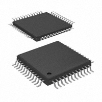
Package: TQFP-48, RoHS compliant
APPLICATIONS
•
•
•
•
•
•
•
•
Digital Audio Recorders and
Mixing Desks
Digital Live Sound Consoles
Digital Audio Effects Processors
Surround Sound Encoders
Broadcast Studio Equipment
Data Acquisition and
Measurement Systems
Audio Test Systems
Sonar
blank
1
2
3
4
Please be aware that an important notice concerning availability, standard warranty, and use in critical applications of Texas
Instruments semiconductor products and disclaimers thereto appears at the end of this data sheet.
Windows is a registered trademark of Microsoft Corporation.
I2S is a trademark of NXP Semiconductor.
All other trademarks are the property of their respective owners.
PRODUCTION DATA information is current as of publication date.
Products conform to specifications per the terms of the Texas
Instruments standard warranty. Production processing does not
necessarily include testing of all parameters.
Copyright © 2006–2009, Texas Instruments Incorporated
�PCM4220
SBAS407C – DECEMBER 2006 – REVISED AUGUST 2009............................................................................................................................................. www.ti.com
DESCRIPTION
The PCM4220 is a high-performance, two-channel analog-to-digital (A/D) converter designed for use in
professional audio applications. Offering outstanding dynamic performance, the PCM4220 provides 24-bit linear
PCM output data, with support for output word length reduction to 20-, 18-, or 16-bits. The PCM4220 includes
three sampling modes, supporting output sampling rates from 8kHz to 216kHz. The PCM4220 is ideal for a
variety of digital audio recording and processing applications.
A linear phase digital decimation filtering engine supports Classic and Low Group Delay filter responses, allowing
optimization for either studio or live sound applications. In addition, digital high-pass filtering is provided for DC
offset removal. The The PCM4220 is configured using dedicated control pins for selection of sampling modes,
audio data formats and word length, decimation filter response, high-pass filter disable, and reset/power-down
functions.
While providing uncompromising performance, the PCM4220 addresses power concerns with just over 300mW
typical total power dissipation, making the device suitable for multi-channel audio systems. The PCM4220 is
typically powered from a +4.0V analog supply and a +3.3V digital supply. The digital I/O is logic-level compatible
with common digital signal processors, digital interface transmitters, and programmable logic devices. The
PCM4220 is available in a TQFP-48 package, which is RoHS-compliant.
This integrated circuit can be damaged by ESD. Texas Instruments recommends that all integrated circuits be handled with
appropriate precautions. Failure to observe proper handling and installation procedures can cause damage.
ESD damage can range from subtle performance degradation to complete device failure. Precision integrated circuits may be more
susceptible to damage because very small parametric changes could cause the device not to meet its published specifications.
ORDERING INFORMATION
For the most current package and ordering information, see the Package Option Addendum at the end of this
data sheet, or see the TI website at www.ti.com
ABSOLUTE MAXIMUM RATINGS (1)
Over operating free-air temperature range, unless otherwise noted.
VALUE
Power supplies
VCC1, VCC2
–0.3V to +6.0V
VDD
–0.3V to +4.0V
Digital input voltage
All digital input and I/O pins
–0.3V < (VDD + 0.3V) < +4.0V
Analog input voltage
VINL+, VINL–, VINR+, VINR–
–0.3V < (VCC + 0.3V) < +6.0V
Input current (all pins except power and ground)
±10mA
Ambient operating temperature
–40°C to +85°C
Storage temperature
(1)
2
–65°C to +150°C
These limits are stress ratings only. Stresses beyond these limits may result in permanent damage. Extended exposure to absolute
maximum ratings may degrade device reliability. Normal operation or performance at or beyond these limits is not specified or ensured.
Submit Documentation Feedback
Copyright © 2006–2009, Texas Instruments Incorporated
Product Folder Link(s): PCM4220
�PCM4220
www.ti.com............................................................................................................................................. SBAS407C – DECEMBER 2006 – REVISED AUGUST 2009
ELECTRICAL CHARACTERISTICS: DIGITAL AND DYNAMIC PERFORMANCE
All specifications are at TA = +25°C, VCC1 = VCC2 = +4.0V, and VDD = +3.3V, unless otherwise noted.
PCM4220
PARAMETER
CONDITIONS
MIN
TYP
MAX
UNIT
VDD
V
DIGITAL I/O CHARACTERISTICS
(Applies to all digital pins)
High-level input voltage, VIH
0.7 × VDD
Low-level input voltage, VIL
0
High-level input current, IIH
1
0.3 × VDD
V
10
µA
10
µA
High-level output voltage, VOH
IO = –2mA
0.8 × VDD
VDD
V
Low-level output voltage, VOL
IO = +2mA
0
0.2 × VDD
Low-level input current, IIL
1
Input capacitance, CIN
3
V
pF
PCM OUTPUT SAMPLING RATE, fS
Normal mode
8
54
kHz
Double Speed mode
54
108
kHz
Quad Speed mode
108
216
kHz
Normal mode, MCKI = 256fS
2.048
13.824
MHz
Double Speed mode, MCKI = 128fS
6.912
13.824
MHz
Quad Speed mode, MCKI = 64fS
6.912
13.824
MHz
–100
dB
MASTER CLOCK INPUT
DYNAMIC PERFORMANCE (1)
PCM Output, Normal Mode, fS = 48kHz
BW = 22Hz to 20kHz
Total harmonic distortion + noise (THD+N)
f = 997Hz, –1dB input
–108
f = 997Hz, –20dB input
–100
dB
f = 997Hz, –60dB input
–61
dB
Dynamic range, no weighting
f = 997Hz, –60dB input
121
dB
Dynamic range, A-weighted
f = 997Hz, –60dB input
118
123
dB
Channel separation
f = 10kHz, –1dB input
115
135
dB
PCM Output, Double Speed Mode, fS = 96kHz
BW = 22Hz to 40kHz
Total harmonic distortion + noise (THD+N)
f = 997Hz, –1dB input
–108
dB
f = 997Hz, –20dB input
–98
dB
f = 997Hz, –60dB input
–58
dB
Dynamic range, no weighting
f = 997Hz, –60dB input
118
dB
Dynamic range, A-weighted
f = 997Hz, –60dB input
123
dB
Channel separation
f = 10kHz, –1dB input
135
dB
PCM Output, Quad Speed Mode, fS = 192kHz
BW = 22Hz to 40kHz
Total harmonic distortion + noise (THD+N)
f = 997Hz, –1dB input
–107
dB
f = 997Hz, –20dB input
–98
dB
f = 997Hz, –60dB input
–58
dB
Dynamic range, no weighting
f = 997Hz, –60dB input
118
dB
Dynamic range, A-weighted
f = 997Hz, –60dB input
123
dB
Channel separation
f = 10kHz, –1dB input
135
dB
PCM Output, Quad Speed Mode, fS = 192kHz
BW = 22Hz to 80kHz
Total harmonic distortion + noise (THD+N)
f = 997Hz, –1dB input
–106
dB
f = 997Hz, –20dB input
–91
dB
f = 997Hz, –60dB input
–52
dB
Dynamic range, no weighting
f = 997Hz, –60dB input
112
dB
Dynamic range, A-weighted
f = 997Hz, –60dB input
123
dB
f = 10kHz, –1dB input
135
dB
Channel separation
(1)
Typical PCM output performance is measured and characterized with an Audio Precision SYS-2722 192kHz test system and a
PCM4222EVM evaluation module modified for use with the PCM4220. Measurement bandwidth and weighting settings are noted in the
Parameter and Conditions columns. THD+N is measured without the use of weighting filters. Master mode operation is utilized for all
typical performance parameters, with the master clock input frequency (MCKI) set to 12.288MHz.
Submit Documentation Feedback
Copyright © 2006–2009, Texas Instruments Incorporated
Product Folder Link(s): PCM4220
3
�PCM4220
SBAS407C – DECEMBER 2006 – REVISED AUGUST 2009............................................................................................................................................. www.ti.com
ELECTRICAL CHARACTERISTICS: DIGITAL AND DYNAMIC PERFORMANCE (continued)
All specifications are at TA = +25°C, VCC1 = VCC2 = +4.0V, and VDD = +3.3V, unless otherwise noted.
PCM4220
PARAMETER
CONDITIONS
MIN
TYP
MAX
UNIT
0.4535 × fS
Hz
±0.00015
dB
Digital Decimation Filter Characteristics:
Classic Response
Passband
Passband ripple
Stop band
0.5465 × fS
Stop band attenuation
Hz
–100
dB
Group delay
39/fS
Seconds
Digital Decimation Filter Characteristics:
Low Group Delay Response
Passband
Passband ripple
Stop band
0.4167 × fS
Hz
±0.001
dB
0.5833 × fS
Stop band attenuation
Hz
–90
dB
Group delay
21/fS
Seconds
Digital High-Pass Filter Characteristics
–3dB corner frequency
High-pass filter enabled
fS/48000
Hz
ELECTRICAL CHARACTERISTICS: ANALOG INPUTS, OUTPUTS, AND DC ERROR
All specifications are at TA = +25°C, VCC1 = VCC2 = +4.0V, and VDD = +3.3V, unless otherwise noted.
PCM4220
PARAMETER
CONDITIONS
MIN
TYP
MAX
UNIT
ANALOG INPUTS
Full-scale input range
Differential input
Per input pin
Input impedance
Referenced from VINL+ to VINL–, or VINR+ to
VINR–
5.6
VPP
Applies to VINL+, VINL–, VINR+, or VINR–
2.8
VPP
Applies to VINL+, VINL–, VINR+, or VINR–
2.8
kΩ
100
dB
V
Common-mode rejection
ANALOG OUTPUTS
Common-mode output voltage
Left channel, VCOML
Measured from VCOML to AGND
0.4875 × VCC2
Right channel, VCOMR
Measured from VCOMR to AGND
0.4875 × VCC1
Common-mode output current
Applies to VCOML or VCOMR
V
200
µA
DC ERROR
Output offset error
Digital high-pass filter disabled
3
mV
Offset drift
Digital high-pass filter disabled
3.5
µV/°C
4
Submit Documentation Feedback
Copyright © 2006–2009, Texas Instruments Incorporated
Product Folder Link(s): PCM4220
�PCM4220
www.ti.com............................................................................................................................................. SBAS407C – DECEMBER 2006 – REVISED AUGUST 2009
ELECTRICAL CHARACTERISTICS: POWER SUPPLIES
All specifications are at TA = +25°C, VCC1 = VCC2 = +4.0V, VDD = +3.3V, and MCKI = 12.288MHz, unless otherwise noted.
PCM4220
PARAMETER
CONDITIONS
MIN
TYP
MAX
UNIT
VCC1, VCC2
0°C 10MW)
To
Bias Nodes
R
VCOML
or
(Optional)
VCOMR
Precision, Low-Noise Op Amp
(OPA227 or equivalent)
100nF to 1mF
Close to IC pins
Figure 37. Common-Mode Output Connections
Submit Documentation Feedback
Copyright © 2006–2009, Texas Instruments Incorporated
Product Folder Link(s): PCM4220
17
�PCM4220
SBAS407C – DECEMBER 2006 – REVISED AUGUST 2009............................................................................................................................................. www.ti.com
MASTER CLOCK INPUT
The PCM4220 requires a master clock for operating the internal logic and modulator circuitry. The master clock
is supplied from an external source, connected at the MCKI input (pin 35). Table 1 summarizes the requirements
for various operating modes of the PCM4220. Referring to Table 1, the term fS refers to the PCM4220 PCM
output sampling rate (that is, 48kHz, 96kHz, 192kHz, etc.). Refer to the Electrical Characteristics table for timing
specifications related to the master clock input.
For best performance, the master clock jitter should be maintained below 40ps peak amplitude.
Table 1. Master Clock Requirements
OPERATING MODE
REQUIRED MASTER CLOCK (MCKI) RATE
PCM Normal
256fS
PCM Double Speed
128fS
PCM Quad Speed
64fS
RESET AND POWER-DOWN OPERATION
The PCM4220 includes an external reset input, RST (pin 36), which may be utilized to force an internal reset
initialization or power-down sequence. The reset input is active low. Figure 38 shows the required timing for an
external forced reset.
A power-down state for the PCM422 may be initiated by forcing and holding the reset input low for the duration
of the desired power-down condition. Minimum power is consumed during this state when all clock inputs for the
PCM4220 are forced low. Before releasing the reset input by forcing a high state, the master clock should be
enabled so that the PCM4220 can execute a reset initialization sequence.
While the RST pin is forced low, or during reset initialization, the audio serial port data and clock outputs are
driven low.
40ns minimum
RST
0V
Internal
Reset
0V
1024 System CLock Periods
Required for Initialization
MCKI
0V
Figure 38. External Reset Sequence
DISABLED STATES FOR THE PCM4220 AUDIO SERIAL PORT
When PCMEN (pin 16) is driven low, the PCM output is disabled. The audio serial port data and clocks are
driven low.
18
Submit Documentation Feedback
Copyright © 2006–2009, Texas Instruments Incorporated
Product Folder Link(s): PCM4220
�PCM4220
www.ti.com............................................................................................................................................. SBAS407C – DECEMBER 2006 – REVISED AUGUST 2009
PCM OUTPUT AND SAMPLING MODES
The PCM4220 supports 24-bit linear PCM output data when the PCMEN input (pin 16) is forced high. The PCM
output is disabled when PCMEN is forced low. The 24-bit output data may be dithered to 20-, 18-, or 16-bits
using internal word length reduction circuitry. Refer to the Output Word Length Reduction section of this data
sheet for additional information.
The PCM4220 supports three PCM sampling modes, referred to as Normal, Double Speed, and Quad Speed.
The sampling mode is determined by the state of the FS0 and FS1 inputs (pins 19 and 20, respectively). Table 2
summarizes the sampling modes available for the PCM4220.
Normal sampling mode supports output sampling rates from 8kHz to 54kHz. The ΔΣ modulator operates with
128x oversampling in this mode. Both the Classic and Low Group Delay decimation filter responses are available
in Normal mode. The master clock (MCKI) rate must be 256x the desired output sampling rate for Normal
operation.
The Double Speed sampling mode supports output sampling rates from 54kHz to 108kHz. The delta-sigma
modulator operates with 64x oversampling in this mode. Both the Classic and Low Group Delay decimation filter
responses are available in Double Speed mode. The master clock (MCKI) rate must be 128x the desired output
sampling rate for Double Speed operation.
Quad Speed sampling mode supports output sampling rates from 108kHz to 216kHz. The delta-sigma modulator
operates with 32x oversampling in this mode. Only the Low Group Delay decimation filter response is available in
Quad Speed mode. The master clock (MCKI) rate must be 64x the desired output sampling rate for Quad Speed
operation.
Table 2. PCM Sampling Mode Configuration
FS1 (pin 20)
FS0 (pin 19)
SAMPLING MODE
LO
LO
Normal, 8kHz ≤ fS ≤ 54kHz
LO
HI
Double Speed, 54kHz < fS ≤ 108kHz
HI
LO
Quad Speed, 108kHz < fS ≤ 216kHz
HI
HI
Reserved
AUDIO SERIAL PORT INTERFACE
The PCM output mode supports a three-wire synchronous serial interface. This interface includes a serial data
output (DATA, pin 32), a serial bit or data clock (BCK, pin 33), and a left/right word clock (LRCK, pin 34). The
BCK and LRCK clock pins may be inputs or outputs, depending on the Slave or Master mode configuration.
Figure 39 illustrates Slave and Master mode serial port connections to an external audio signal processor or host
device.
The audio serial port supports four data formats that are illustrated in Figure 40, Figure 42, and Figure 43. The
I2S and Left-Justified formats support two channels of audio output data. The TDM data formats can support up
to eight channels of audio output data on a single data line. The audio data format is selected using the FMT0
and FMT1 inputs (pins 44 and 43, respectively). Table 3 summarizes the audio data format options. For all
formats, audio data are represented as two’s complement binary data, with the MSB transmitted first. Regardless
of the format selection, audio data are always clocked out of the port on the falling edge of the BCK clock.
Table 3. PCM Audio Data Format Selection
FMT1 (pin 43)
FMT0 (pin 44)
AUDIO DATA FORMAT
LO
LO
Left-Justified
LO
HI
I2S
HI
LO
TDM
HI
HI
TDM with data delayed one BCK cycle from LRCK rising edge
The LRCK clock rate should always be operated at the desired output sampling rate, or fS. In Slave mode, the
LRCK clock is an input, with the rate set by an external audio bus master (that is, a clock generator, digital signal
processor, etc.). In Master mode, the LRCK clock is an output, derived from the master clock input using on-chip
clock dividers (as is the BCK clock). The clock divider is configured using the FS0 and FS1 pins, which are
discussed in the PCM Output and Sampling Modes section of this datasheet.
Submit Documentation Feedback
Copyright © 2006–2009, Texas Instruments Incorporated
Product Folder Link(s): PCM4220
19
�PCM4220
SBAS407C – DECEMBER 2006 – REVISED AUGUST 2009............................................................................................................................................. www.ti.com
For the I2S and Left-Justified data formats, the BCK clock output rate is fixed in Master mode, with the Normal
mode being 128fS and the Double and Quad Speed modes being 64fS. In Slave Mode, a BCK clock input rate of
64fS or 128fS is recommended for Normal mode, while 64fS is recommended for Double and Quad Rate modes.
For the TDM data formats, the BCK rate depends upon the sampling mode for either Slave or Master operation.
For Normal sampling, the BCK must be 256fS. Double Speed mode requires 128fS, while Quad Speed mode
requires 64fS. This requirement limits the maximum number of channels carried by the TDM formats to eight for
Normal mode, four for Double Rate mode, and two for Quad Rate mode.
When using the TDM formats, the sub-frame assignment for the device must be selected using the SUB0 and
SUB1 inputs (pins 26 and 25, respectively). Table 4 summarizes the sub-frame selection options. A sub-frame
contains two 32-bit time slots, with each time slot carrying 24 bits of audio data corresponding to either the left or
right channel of the PCM4220. Refer to Figure 41 through Figure 43 for TDM interfacing connections and
sub-frame formatting details. For the TDM format with one BCK delay, the serial data output is delayed by one
BCK period after the rising edge of the LRCK clock.
Table 4. TDM Sub-frame Assignment
SUB1 (pin 25)
SUB0 (pin 26)
SUB-FRAME ASSIGNMENT
LO
LO
Sub-frame 0
LO
HI
Sub-frame 1
HI
LO
Sub-frame 2
HI
HI
Sub-frame 3
When using TDM formats with Double Speed sampling, it is recommended that the SUB1 pin be forced low.
When using TDM formats with Quad Speed sampling, it is recommended that both the SUB0 and SUB1 pins be
forced low.
For all serial port modes and data formats, when driving capacitive loads greater than 30pF with the data and
clock outputs, it is recommended that external buffers be utilized to ensure data and clock integrity at the
receiving device(s).
For specifications regarding audio serial port operation, the reader is referred to the Electrical Characteristics:
Audio Interface Timing table, as well as Figure 1 and Figure 2 in this data sheet.
Audio DSP
or
Interface
PCM4220
LRCK
FSYNC
Audio DSP
or
Interface
PCM4220
LRCK
FSYNC
BCK
SCLK
BCK
SCLK
DATA
DATA
DATA
DATA
MCKI
MCLK
MCKI
Master
Clock
(a) Slave Mode (S/M = HI)
MCLK
Master
Clock
(b) Master Mode (S/M = LO)
Figure 39. Slave and Master Mode Operation
20
Submit Documentation Feedback
Copyright © 2006–2009, Texas Instruments Incorporated
Product Folder Link(s): PCM4220
�PCM4220
www.ti.com............................................................................................................................................. SBAS407C – DECEMBER 2006 – REVISED AUGUST 2009
Left Channel
Right Channel
LRCK
BCK
DATA
MSB
LSB
MSB
LSB
(a) Left-Justified Data Format
LRCK
BCK
MSB
DATA
LSB
MSB
LSB
2
(b) I S Data Format
1/fS
Figure 40. Left-Justified and I2S Data Formats
PCM4220
(sub-frame 0)
Slave
LO
LO
SUB0
SUB1
PCM4220
(sub-frame 1)
Slave
HI
LO
LRCK
BCK DATA
SUB0
SUB1
PCM4220
(sub-frame 2)
Slave
LO
HI
SUB0
SUB1
PCM4220
(sub-frame 3)
Slave
HI
HI
SUB0
SUB1
LRCK
BCK DATA
LRCK
BCK DATA
LRCK
BCK DATA
PCM4220
(sub-frame 1)
Slave
PCM4220
(sub-frame 2)
Slave
PCM4220
(sub-frame 3)
Slave
LRCK
BCK
DATA
(a) All devices are Slaves.
PCM4220
(sub-frame 0)
Master
LO
LO
SUB0
SUB1
LRCK
BCK DATA
HI
LO
SUB0
SUB1
LRCK
BCK DATA
LO
HI
SUB0
SUB1
LRCK
BCK DATA
HI
HI
SUB0
SUB1
LRCK
BCK DATA
LRCK
BCK
DATA
(b) One device is the Master while all other devices are Slaves.
Figure 41. TDM Mode Interface Connections (PCM Normal Mode Shown)
Submit Documentation Feedback
Copyright © 2006–2009, Texas Instruments Incorporated
Product Folder Link(s): PCM4220
21
�PCM4220
SBAS407C – DECEMBER 2006 – REVISED AUGUST 2009............................................................................................................................................. www.ti.com
LRCK
Normal Mode
DATA
L
R
L
R
L
R
L
R
Sub-frame 0 Sub-frame 1 Sub-frame 2 Sub-frame 3
One Frame, 1/fS
LRCK
Double Speed Mode
DATA
L
R
L
R
L
R
L
R
Sub-frame 0 Sub-frame 1 Sub-frame 0 Sub-frame 1
One Frame, 1/fS
One Frame, 1/fS
LRCK
Quad Speed Mode
DATA
L
R
L
R
L
R
L
R
One Frame One Frame One Frame One Frame
1/fS
1/fS
1/fS
1/fS
NOTE: Each L or R channel time slot is 32 bits long, with 24-bit data Left-Justified in the time slot. Audio data is MSB first. Sub-frame
assignments for each PCM4220 device are selected by the corresponding SUB0 and SUB1 pin settings.
Figure 42. TDM Data Formats: Slave Mode
LRCK
Normal Mode
DATA
L
R
L
R
L
R
L
R
Sub-frame 0 Sub-frame 1 Sub-frame 2 Sub-frame 3
One Frame, 1/fS
LRCK
Double Speed Mode
DATA
L
R
L
R
L
R
L
R
Sub-frame 0 Sub-frame 1 Sub-frame 0 Sub-frame 1
One Frame, 1/fS
One Frame, 1/fS
LRCK
Quad Speed Mode
DATA
L
R
L
R
L
R
L
R
One Frame One Frame One Frame One Frame
1/fS
1/fS
1/fS
1/fS
NOTE: Each L or R channel time slot is 32 bits long, with 24-bit data Left-Justified in the time slot. Audio data is MSB first. Sub-frame
assignments for each PCM4220 device are selected by the corresponding SUB0 and SUB1 pin settings.
Figure 43. TDM Data Formats: Master Mode
DIGITAL DECIMATION FILTER
The PCM4220 digital decimation filter is a linear phase, multistage finite impulse response (FIR) design with two
user-selectable filter responses. The decimation filter provides the digital downsampling and low-pass anti-alias
filter functions for the PCM4220.
The Classic filter response is typical of traditional audio data converters, with Figure 24 through Figure 27
detailing the frequency response, and the related specifications given in the Electrical Characteristics table. The
group delay for the Classic filter is 39/fS, or 812.5µs for fS = 48kHz and 406.25µs for fS = 96kHz. The Classic filter
response is not available for the Quad Speed sampling mode.
22
Submit Documentation Feedback
Copyright © 2006–2009, Texas Instruments Incorporated
Product Folder Link(s): PCM4220
�PCM4220
www.ti.com............................................................................................................................................. SBAS407C – DECEMBER 2006 – REVISED AUGUST 2009
The Low Group Delay response provides a lower latency option for the decimation filter, and is detailed in
Figure 28 through Figure 31, with the relevant specifications given in the Electrical Characteristics table. The Low
Group Delay filter response is available for all sampling modes. The group delay for this filter is 21/fS, or 437.5µs
for fS = 48kHz, 218.75µs for fS = 96kHz, and 109.375µs for fS = 192kHz.
The decimation filter response is selected using the DF input (pin 21), with the settings summarized in Table 5.
For Quad Speed sampling mode operation, the Low Group Delay filter is always selected, regardless of the DF
pin setting.
Table 5. Decimation Filter Response Selection
DF (pin 21)
DECIMATION FILTER RESPONSE
LO
Classic response, with group delay = 39/fS
HI
Low Group Delay response, with group delay = 21/fS
DIGITAL HIGH-PASS FILTER
The PCM4220 incorporates digital high-pass filters for both the left and right audio channels, with the purpose of
removing the ΔΣ modulator dc offset from the audio output data. Figure 32 and Figure 33 detail the frequency
response for the digital high-pass filter. The f–3dB frequency is approximately fS/48000, where fS is the PCM
output sampling rate.
Two inputs, HPFDR (pin 17) and HPFDL (pin 18), allow the digital high-pass filter to be enabled or disabled
individually for the right and left channels, respectively. Table 6 summarizes the operation of the high-pass filter
disable pins.
Table 6. Digital High-Pass Filter Configuration
HPFDR (pin 17) or HPFDL (pin 18)
HIGH-PASS FILTER STATE
LO
Enabled for the corresponding channel
HI
Disabled for the corresponding channel
PCM OUTPUT WORD LENGTH REDUCTION
The PCM4220 is typically configured to output 24-bit linear PCM audio data. However, internal word length
reduction circuitry may be utilized to reduce the 24-bit data to 20-, 18-, or 16-bit data. This reduction is
accomplished by using a Triangular PDF dithering function. The OWL0 (pin 42) and OWL1 (pin 41) inputs are
utilized to select the output data word length. Table 7 summarizes the output word length configuration options.
Table 7. PCM Audio Data Word Length Selection
OWL1 (pin 41)
OWL0 (pin 42)
OUTPUT WORD LENGTH
LO
LO
24 bits
LO
HI
18 bits
HI
LO
20 bits
HI
HI
16 bits
OVERFLOW INDICATORS
The PCM4220 includes two active-high digital overflow outputs, OVFL (pin 37) and OVFR (pin 38),
corresponding to the left and right channels, respectively. These outputs are functional when the PCM output
mode is enabled, as the overflow detection circuitry is incorporated into the digital filter engine. The overflow
indicators are forced high whenever a digital overflow is detected for a given channel. The overflow indicators
may be utilized as clipping flags, and monitored using a host processor or light-emitting diode (LED) indicators.
When driving a LED, the overflow output may be buffered to ensure adequate drive for the LED. A recommended
buffer is Texas Instruments' SN74LVC1G125. Equivalent buffers may be substituted
Submit Documentation Feedback
Copyright © 2006–2009, Texas Instruments Incorporated
Product Folder Link(s): PCM4220
23
�PCM4220
SBAS407C – DECEMBER 2006 – REVISED AUGUST 2009............................................................................................................................................. www.ti.com
TYPICAL CONNECTIONS
Figure 44 provides a typical connection diagram for the PCM4220. Recommended power-supply bypass and
reference filter capacitors are shown. These components should be located as close to the corresponding
PCM4220 package pins as physically possible. Larger power-supply bypass capacitors may be placed on the
bottom side of the printed circuit board (PCB). However, reference decoupling capacitors should be located on
the top side of the PCB to avoid issues with added via inductance.
As Figure 44 illustrates, the audio host device may be a digital signal processor (DSP), digital audio interface
transmitter (DIT), or a programmable logic device.
PCM4220PFB
1
2
Right Channel
Analog Input
3
100mF
+
100nF
4
+4.0V
AGND
VCOMR
VINR-
REFGNDR
VINR+
VREFR
VCC1
DGND
5
AGND
FMT0
AGND
FMT1
AGND
OWL0
AGND
OWL1
VCC2
DGND
VINL-
S/M
VINL+
OVFR
AGND
OVFL
7
12
13
14
100nF
15
16
+
17
100mF
18
From Host, Logic,
or Manual Controls
19
20
21
22
23
24
100mF
+
From Host, Logic,
or Manual Controls
40
39
11
100nF to 1mF
45
41
10
Left Channel
Analog Input
100nF
46
42
9
+
47
43
8
100mF
100nF to 1mF
44
6
100nF
48
38
VCOML
RST
REFGNDL
MCKI
VREFL
LRCK
PCMEN
BCK
HPFDR
DATA
HPFDL
VDD
FS0
DGND
FS1
NC
DF
NC
DGND
NC
DGND
SUB0
DGND
SUB1
37
36
35
To Host and/or Clipping Indicators
From Host or Master Reset
From Audio Master Clock Source
34
33
32
Audio
DSP or Host
+3.3V
100nF
31
30
100mF
+
29
28
27
26
25
Required only for TDM data formats.
These pins are ignored for all other formats.
Figure 44. Typical Connections for PCM and DSD Output Modes
INPUT BUFFER CIRCUITS
The PCM4220 is typically preceded in an application by an input buffer or preamplifier circuit. The input circuit is
required to perform anti-aliasing filtering, in addition to application-specific analog gain scaling, limiting, or
processing that may be needed. At a minimum, first-order, low-pass anti-aliasing filtering is necessary. The input
buffer must be able to perform the input filtering requirement, in addition to driving the switched-capacitor inputs
of the PCM4220 device. The buffer must have adequate bandwidth, slew rate, settling time, and output drive
capability to perform these tasks.
Figure 45 illustrates the input buffer/filter circuit utilized on the PCM4222EVM evaluation module, where the
PCM4222 analog input section is identical to the PCM4220. This circuit has been optimized for measurement
purposes, so that it does not degrade the dynamic characteristics of the PCM4220. The resistors are primarily
0.1% metal film. The 40.2Ω resistor is 1% tolerance thick film. The 1nF and 2.7nF capacitors may be either PPS
24
Submit Documentation Feedback
Copyright © 2006–2009, Texas Instruments Incorporated
Product Folder Link(s): PCM4220
�PCM4220
www.ti.com............................................................................................................................................. SBAS407C – DECEMBER 2006 – REVISED AUGUST 2009
film or C0G ceramic capacitors; both types perform with equivalent results in this application. Surface-mount
devices are utilized throughout because they provide superior performance when combined with a wideband
amplifier such as the OPA1632. The DGN package version of the OPA1632 is utilized; this package includes a
thermal pad on the bottom side. The thermal pad must be soldered to the PCB ground plane for heat sink and
mechanical support purposes.
270W (0.1%)
1nF
-15V
10nF-100nF
Full-Scale: 11.76VPP Differential
Typical with RS = 40W
6
7
Analog Input
560W (0.1%)
5
40.2W (1%)
OPA1632DGN
40.2W (1%)
8
EN
2
3
560W (0.1%)
1
VOCM
G
VINL- or VINR2.7nF
VINL+ or VINR+
4
2
1
3
From
Buffered VCOM
R
10nF-100nF
100nF
T
S
+15V
Ground
Lift Switch
1nF
270W (0.1%)
Figure 45. Differential Input Buffer Circuit Utilizing the OPA1632
Figure 46 demonstrates the same circuit topology of Figure 45, while using standard single or dual op amps. The
noise level of this circuit is adequate for obtaining the typical A-weighted dynamic range performance for the
PCM4220. However, unweighted performance may suffer, depending upon the op amp noise specifications.
Near-typical THD+N can be achieved with this configuration, although this performance also depends on the op
amps used for the application. The NE5534A and OPA227 (the lower cost 'A' version) are good candidates from
a noise and distortion perspective, and are reasonably priced. More expensive lower-noise models, such as the
OPA211, should also work well for this configuration. Feedback and input resistor values may be changed to
alter circuit gain. However, it is recommended that all circuit changes be simulated and then tested on the bench
using a working prototype to verify performance.
Figure 47 illustrates a differential input circuit that employs a noninverting architecture. The total noise and
distortion is expected to be higher than that measured for Figure 45 and Figure 46. As with Figure 46, the
NE5534A and OPA227 are good candidates for this circuit, although similar op amps should yield equivalent
results.
A useful tool for simulating the circuits shown here is TINA-TI, a free schematic capture and SPICE-based
simulator program available from the Texas Instruments web site. This tool includes macro models for many TI
and Burr-Brown branded amplifiers and analog integrated circuits. TINA-TI runs on personal computers using
Microsoft Windows® operating systems (Windows 2000 or newer).
Submit Documentation Feedback
Copyright © 2006–2009, Texas Instruments Incorporated
Product Folder Link(s): PCM4220
25
�PCM4220
SBAS407C – DECEMBER 2006 – REVISED AUGUST 2009............................................................................................................................................. www.ti.com
270W
1nF
C1
INPUT+
560W
40.2W
+
VINL- or VINR-
U1
VCOML
or
VCOMR
100nF
2.7nF
40.2W
C2
INPUT-
VINL+ or VINR+
U2
560W
+
1nF
270W
U1, U2 = NE5534A, OPA227, or similar
NOTE: C1 and C2 provide ac coupling. They may be removed if the dc offset from the circuit is negligible.
Figure 46. Alternative Buffer Circuit Using Standard Op Amps
1.5kW
1nF
40.2W
C1
INPUT+
R1W
VINL+ or VINR+
U1
+
10kW
2.7nF
10kW
C2
INPUT-
R2W
40.2W
+
VINL- or VINR-
U2
VCOML
or
VCOMR
1nF
U3
1.5kW
U1, U2 = NE5534A, OPA227, or similar.
U3 = OPA227 or equivalent.
NOTE: R1 and R2 are optional. When used, values may be selected for the desired attenuation.
NOTE: C1 and C2 provide ac coupling. They may be removed if the dc offset from the circuit is negligible.
Figure 47. Noninverting Differential Input Buffer Utilizing Standard Op Amps
26
Submit Documentation Feedback
Copyright © 2006–2009, Texas Instruments Incorporated
Product Folder Link(s): PCM4220
�PCM4220
www.ti.com............................................................................................................................................. SBAS407C – DECEMBER 2006 – REVISED AUGUST 2009
INTERFACING TO DIGITAL AUDIO TRANSMITTERS (AES3, IEC60958-3, and S/PDIF)
The serial output of audio analog-to-digital converters is oftentimes interfaced to transmitter devices that encode
the serial output data to either the AES3 or IEC60958-3 (or S/PDIF) interface formats. Texas Instruments
manufactures several devices that perform this encoding, including the DIT4192, DIX4192, SRC4382, and
SRC4392. This section describes and illustrates the audio serial port interface connections required for
communications between the PCM4220 and these devices. Register programming details for the DIX4192 and
SRC4382/4392 are also provided.
Figure 48 shows the interface between a PCM4220 and a DIT4192 transmitter. This configuration supports
sampling frequencies and encoded frame rates from 8kHz to 216kHz. For this example, the audio data format
must be either Left-Justified or I2S; TDM formats are not supported by the DIT4192. In addition, the PCM4220
VDD supply and DIT4192 VIO supply must be the same voltage, to ensure logic level compatibility.
Figure 49 illustrates the audio serial port interface between the PCM4220 and either a DIX4192 transceiver or
SRC4382/SRC4392 combo sample rate converter/transceiver device. Port A of the DIX4192 or
SRC4382/SRC4392 is utilized for this example. Data acquired by Port A are sent on to the DIT function block
within the interface device for AES3 encoding and transmission.
The DIX4192 and SRC4382/SRC4392 are software-configurable, with control register and data buffer settings
that determine the operation of internal function blocks. Table 8 and Table 9 summarize the control register
settings for the Port A and the DIT function blocks for both A/D Converter Master and Slave modes, respectively.
Input sampling and encoded frame rates from 8kHz to 216kHz are supported with the appropriate register
settings.
Master
Clock
512fS (Normal)
256fS (Double Speed)
128fS (Quad Speed)
Divided by 2
PCM4220
MCKI
FS1
DIT4192
BCK
SCLK
LRCK
SYNC
DATA
SDATA
FS0
FS0
LO
HI
LO
HI
Mode
Normal
Double Speed
Quad Speed
Reserved
CLK0
CLK1
S/M
FS1
LO
LO
HI
HI
MCLK
M/S
CLK1
LO
LO
HI
HI
LO = ADC Master
HI = ADC Slave
CLK0
LO
HI
LO
HI
Mode
Quad Speed
Double Speed
Reserved
Normal
Figure 48. Interfacing the PCM4220 to a DIT4192
Submit Documentation Feedback
Copyright © 2006–2009, Texas Instruments Incorporated
Product Folder Link(s): PCM4220
27
�PCM4220
SBAS407C – DECEMBER 2006 – REVISED AUGUST 2009............................................................................................................................................. www.ti.com
DIX4192
or
SRC4392
PCM4220
BCK
BCKA
LRCK
LRCKA
DATA
SDINA
MCKI
MCLK
Divided by 2
512fS (Normal)
256fS (Double Speed)
128fS (Quad Speed)
Master
Clock
NOTE: VDDPCM4220 = VIODIX4192 or SRC4392.
Audio data format if I2S or Left Justified.
Interface supports ADC Slave or Master configurations, depending on DIX4192, SRC4382, or SRC4392 register setup.
Figure 49. Interfacing the PCM4220 to a DIX4192, SRC4382, or SRC4392
Table 8. Register Configuration Sequence for an ADC Master Mode Interface
REGISTER ADDRESS (hex)
REGISTER DATA (hex)
COMMENTS
7F
00
Select Register Page 0
03
00
01
Port A is Slave mode with Left-Justified audio data format, or
Port A is Slave mode with I2S Data format
04
00
Default for Port A Slave mode operation
07
64
24
04
Divide MCLK by 512 for Normal sampling, or
Divide MCLK by 256 for Double Speed Sampling, or
Divide MCLK by 128 for Quad Speed sampling
08
00
Line Driver and AESOUT buffer enabled
09
01
Data buffers on Register Page 2 are the source for the DIT channel
status (C) and user (U) data
01
34
Power up Port A and the DIT
Table 9. Register Configuration Sequence for an ADC Slave Mode Interface
28
REGISTER ADDRESS (hex)
REGISTER DATA (hex)
COMMENTS
7F
00
Select Register Page 0
03
08
09
Port A is Master mode with Left-Justified audio data format, or
Port A is Master mode with I2S Data format
04
03
01
00
Divide MCLK by 512 for Normal sampling, or
Divide MCLK by 256 for Double Speed sampling, or
Divide MCLK by 128 for Quad Speed sampling
07
64
24
04
Divide MCLK by 512 for Normal sampling, or
Divide MCLK by 256 for Double Speed Sampling, or
Divide MCLK by 128 for Quad Speed sampling
08
00
Line Driver and AESOUT buffer enabled
09
01
Data buffers on Register Page 2 are the source for the DIT channel
status (C) and user (U) data
01
34
Power up Port A and the DIT
Submit Documentation Feedback
Copyright © 2006–2009, Texas Instruments Incorporated
Product Folder Link(s): PCM4220
�PCM4220
www.ti.com............................................................................................................................................. SBAS407C – DECEMBER 2006 – REVISED AUGUST 2009
The DIT channel status (C) and user (U) data bits in register page 2 may be programmed after the DIT block has
powered up. To program these bits, disable buffer transfers by setting the BTD bit in control register 0x08 to '1'.
Then, select register page 2 using register address 0x7F. You can now load the necessary C and U data
registers for the intended application by writing the corresponding data buffer addresses. When you have
finished writing the C and U data, select register page 0 using register address 0x7F. Re-enable buffer transfers
by setting the BTD bit in control register 0x08 to '0'.
Submit Documentation Feedback
Copyright © 2006–2009, Texas Instruments Incorporated
Product Folder Link(s): PCM4220
29
�PCM4220
SBAS407C – DECEMBER 2006 – REVISED AUGUST 2009............................................................................................................................................. www.ti.com
Revision History
NOTE: Page numbers for previous revisions may differ from page numbers in the current version.
Changes from Revision B (October 2007) to Revision C ............................................................................................... Page
•
Corrected statement concerning direction to drive PCMEN (pin 16) to disable PCM output .............................................. 18
Changes from Revision A (May 2007) to Revision B ...................................................................................................... Page
•
•
30
Changed Figure 26 y-axis value from (dB) to (db/10,000) .................................................................................................. 12
Changed Figure 30 y-axis value from (dB) to (db/1000) ..................................................................................................... 13
Submit Documentation Feedback
Copyright © 2006–2009, Texas Instruments Incorporated
Product Folder Link(s): PCM4220
�PACKAGE OPTION ADDENDUM
www.ti.com
10-Dec-2020
PACKAGING INFORMATION
Orderable Device
Status
(1)
Package Type Package Pins Package
Drawing
Qty
Eco Plan
(2)
Lead finish/
Ball material
MSL Peak Temp
Op Temp (°C)
Device Marking
(3)
(4/5)
(6)
PCM4220PFB
ACTIVE
TQFP
PFB
48
250
RoHS & Green
NIPDAU
Level-3-260C-168 HR
-40 to 85
PCM4220
PCM4220PFBR
ACTIVE
TQFP
PFB
48
1000
RoHS & Green
NIPDAU
Level-3-260C-168 HR
-40 to 85
PCM4220
(1)
The marketing status values are defined as follows:
ACTIVE: Product device recommended for new designs.
LIFEBUY: TI has announced that the device will be discontinued, and a lifetime-buy period is in effect.
NRND: Not recommended for new designs. Device is in production to support existing customers, but TI does not recommend using this part in a new design.
PREVIEW: Device has been announced but is not in production. Samples may or may not be available.
OBSOLETE: TI has discontinued the production of the device.
(2)
RoHS: TI defines "RoHS" to mean semiconductor products that are compliant with the current EU RoHS requirements for all 10 RoHS substances, including the requirement that RoHS substance
do not exceed 0.1% by weight in homogeneous materials. Where designed to be soldered at high temperatures, "RoHS" products are suitable for use in specified lead-free processes. TI may
reference these types of products as "Pb-Free".
RoHS Exempt: TI defines "RoHS Exempt" to mean products that contain lead but are compliant with EU RoHS pursuant to a specific EU RoHS exemption.
Green: TI defines "Green" to mean the content of Chlorine (Cl) and Bromine (Br) based flame retardants meet JS709B low halogen requirements of


 工商网监
湘ICP备2023018690号
工商网监
湘ICP备2023018690号
