Product
Folder
Sample &
Buy
Support &
Community
Tools &
Software
Technical
Documents
TLC59116F
SCLS714C – MARCH 2009 – REVISED SEPTEMBER 2015
TLC59116F 16-Channel Fast-Mode Plus I2C Bus LED Driver
1 Features
•
1
•
•
•
•
•
•
•
•
•
•
•
•
•
•
•
•
1
16 LED Drivers (Each Output Programmable at
OFF, ON, LED Brightness, and Group
Dimming/Blinking Mixed With Individual LED
Brightness)
16 Open-Drain Output Channels
256-Step (8-Bit) Linear Programmable Brightness
Per LED Output Varying From Fully OFF (Default)
to Maximum Brightness Using a 97-kHz PWM
Signal
256-Step Group Brightness Control Allows
General Dimming (Using a 190-Hz PWM Signal
From Fully OFF to Maximum Brightness (Default)
256-Step Group Blinking With Frequency
Programmable From 24 Hz to 10.73 s and Duty
Cycle from 0% to 99.6%
Four Hardware Address Pins Allow 14
TLC59116F Devices to be Connected to the
Same I2C Bus
Four Software-Programmable I2C Bus Addresses
(One LED Group Call Address and Three LED
Sub-Call Addresses) Allow Groups of Devices to
be Addressed Simultaneously in Any Combination
(For example, One Register Used for 'All Call' So
All the TLC59116Fs on the I2C Bus Can be
Addressed at the Same Time and the Second
Register Used for Three Different Addresses So
That 1/3 of all Devices on the Bus Can Be
Addressed at the Same Time in a Group).
Software Enable and Disable for I2C Bus Address.
Software Reset Feature (SWRST Call) Allows the
Device to be Reset Through the I2C Bus
Up to 14 Possible Hardware Adjustable Individual
I2C Bus Addresses Per Device so That Each
Device Can be Programmed
Output State Change Programmable on the
Acknowledge or the STOP Command to Update
Outputs Byte-by-Byte or All at the Same Time
(Default to Change on STOP).
120-mA Maximum Output Current
17-V Maximum Output Voltage
25-MHz Internal Oscillator Requires No External
Components
1-MHz Fast-Mode Plus (FM+) Compatible I2C Bus
Interface With 30 mA High Drive Capability on
SDA Output for Driving High Capacity Buses
Internal Power-On Reset
Noise Filter on SCL/SDA Inputs
No Glitch on Power Up
•
•
•
•
•
•
•
Active-Low Reset
Supports Hot Insertion
Low Standby Current
3.3-V or 5-V Supply Voltage
5.5-V Tolerant Inputs
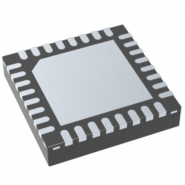
28-Pin TSSOP (PW)
–40°C to 85°C Operation
2 Applications
•
•
•
Gaming
Small Signage
Industrial Equipment
3 Description
The TLC59116F is an I2C-bus controlled 16-channel
LED driver optimized for red/green/blue/amber
(RGBA) color mixing applications. Each LED output
has its own 8-bit resolution (256 steps) fixed
frequency individual PWM controller that operates at
97 kHz with a duty cycle that is adjustable from 0% to
99.6% to allow the LED to be set to a specific
brightness value. An additional 8-bit resolution (256
steps) group PWM controller has both a fixed
frequency of 190 Hz and an adjustable frequency
between 24 Hz to once every 10.73 seconds with a
duty cycle that is adjustable from 0% to 99.6% that is
used to either dim or blink all LEDs with the same
value.
Device Information
PART NUMBER
TLC59116F
PACKAGE
(1)
BODY SIZE (NOM)
TSSOP (28)
9.70 mm × 4.40 mm
VQFN (32)
5.00 mm × 5.00 mm
(1) For all available packages, see the orderable addendum at
the end of the datasheet.
Application Schematic
VLED
3.3V or 5V
µC
SCL
VDD
SDA
OUT15
RESET
A0-A3
OUT0
TLC59116F
GND
An IMPORTANT NOTICE at the end of this data sheet addresses availability, warranty, changes, use in safety-critical applications,
intellectual property matters and other important disclaimers. PRODUCTION DATA.
�TLC59116F
SCLS714C – MARCH 2009 – REVISED SEPTEMBER 2015
www.ti.com
Table of Contents
1
2
3
4
5
6
7
8
Features ..................................................................
Applications ...........................................................
Description .............................................................
Revision History.....................................................
Pin Configuration and Functions .........................
Specifications.........................................................
1
1
1
2
3
4
6.1
6.2
6.3
6.4
6.5
6.6
6.7
4
4
4
4
5
6
7
Absolute Maximum Ratings .....................................
ESD Ratings..............................................................
Recommended Operating Conditions ......................
Thermal Information ..................................................
Electrical Characteristics...........................................
I2C Interface Bus Timing Requirements ...................
Typical Characteristics ..............................................
Parameter Measurement Information .................. 7
Detailed Description .............................................. 9
8.1 Overview ................................................................... 9
8.2 Functional Block Diagram ......................................... 9
8.3
8.4
8.5
8.6
9
Feature Description.................................................
Device Functional Modes........................................
Programming...........................................................
Register Maps .........................................................
10
11
11
16
Application and Implementation ........................ 23
9.1 Application Information............................................ 23
9.2 Typical Application ................................................. 24
10 Power Supply Recommendations ..................... 26
11 Layout................................................................... 26
11.1 Layout Guidelines ................................................. 26
11.2 Layout Examples................................................... 26
12 Device and Documentation Support ................. 28
12.1
12.2
12.3
12.4
Community Resources..........................................
Trademarks ...........................................................
Electrostatic Discharge Caution ............................
Glossary ................................................................
28
28
28
28
13 Mechanical, Packaging, and Orderable
Information ........................................................... 28
4 Revision History
NOTE: Page numbers for previous revisions may differ from page numbers in the current version.
Changes from Revision B (July 2011) to Revision C
Page
•
Added Pin Configuration and Functions section, ESD Ratings table, Feature Description section, Device Functional
Modes, Application and Implementation section, Power Supply Recommendations section, Layout section, Device
and Documentation Support section, and Mechanical, Packaging, and Orderable Information section .............................. 1
•
Removed Thermal Impedence table from Specifications ...................................................................................................... 5
•
Added Figure 1 and Figure 2 to Typical Characteristics ....................................................................................................... 6
•
Removed Figure 9 from Control Register............................................................................................................................. 16
•
Added Figure 22 and Figure 23 to Layout Examples .......................................................................................................... 26
Changes from Revision A (June 2010) to Revision B
•
2
Page
Changed QFN PIN NO. to fix pin assignment typo. ............................................................................................................... 3
Submit Documentation Feedback
Copyright © 2009–2015, Texas Instruments Incorporated
Product Folder Links: TLC59116F
�TLC59116F
www.ti.com
SCLS714C – MARCH 2009 – REVISED SEPTEMBER 2015
5 Pin Configuration and Functions
25
27
26
29
28
30
32
1
24
2
23
22
3
4
21
Exposed
Thermal Pad
5
20
RESET
GND
OUT15
OUT14
OUT13
OUT12
GND
OUT11
16
15
14
17
13
8
11
19
18
12
6
7
9
A2
A3
OUT0
OUT1
OUT2
OUT3
GND
OUT4
31
VCC
SDA
SCL
RESET
GND
OUT15
OUT14
OUT13
OUT12
GND
OUT11
OUT10
OUT9
OUT8
10
28
27
26
25
24
23
22
21
20
19
18
17
16
15
1
2
3
4
5
6
7
8
9
10
11
12
13
14
OUT5
OUT6
OUT7
N.C.
N.C.
OUT8
OUT9
OUT10
N.C.
A0
A1
A2
A3
OUT0
OUT1
OUT2
OUT3
GND
OUT4
OUT5
OUT6
OUT7
RHB Package
32-Pin VQFN
Top View
A1
A0
N.C.
N.C.
N.C.
VCC
SDA
SCL
PW Package
28-Pin TSSOP
Top View
If used, the exposed thermal pad must be connected as a secondary ground.
N.C. – No internal connection
Pin Functions
PIN
NAME
I/O
DESCRIPTION
QFN (RHB)
TSSOP (PW)
A0
31
2
I
Address input 0
A1
32
3
I
Address input 1
A2
1
4
I
Address input 2
A3
2
5
I
Address input 3
GND
7, 18, 23
10, 19, 24
–
Power ground
N.C.
12, 13, 28, 29, 30
1
–
No internal connection
3–6
6–9
O
Open-drain output 0 to 3, LED ON at low
8–11
11–14
O
Open-drain output 4 to 7, LED ON at low
14–17
15–18
O
Open-drain output 8 to 11, LED ON at low
19–22
20–23
O
Open-drain output 12 to 15, LED ON at low
RESET
24
25
I
Active-low reset input
SCL
25
26
I
Serial clock input
SDA
26
27
I/O
VCC
27
28
–
OUT0
OUT1
OUT2
OUT3
OUT4
OUT5
OUT6
OUT7
OUT8
OUT9
OUT10
OUT11
OUT12
OUT13
OUT14
OUT15
Serial data input/output
Power supply
Submit Documentation Feedback
Copyright © 2009–2015, Texas Instruments Incorporated
Product Folder Links: TLC59116F
3
�TLC59116F
SCLS714C – MARCH 2009 – REVISED SEPTEMBER 2015
www.ti.com
6 Specifications
6.1 Absolute Maximum Ratings
over operating free-air temperature range (unless otherwise noted) (see
(1)
)
MIN
MAX
UNIT
0
7
V
–0.4
7
V
–0.5
20
V
120
mA
VCC
Supply voltage
VI
Input voltage
VO
Output voltage
IO
Continuous output current per channel
PD
Power dissipation (TA = 25°C, JESD 51-7)
1.6
W
TJ
Junction temperature
–40
150
°C
Tstg
Storage temperature
–55
150
°C
(1)
PW package
Stresses beyond those listed under Absolute Maximum Ratings may cause permanent damage to the device. These are stress ratings
only, which do not imply functional operation of the device at these or any other conditions beyond those indicated under Recommended
Operating Conditions . Exposure to absolute-maximum-rated conditions for extended periods may affect device reliability.
6.2 ESD Ratings
VALUE
Electrostatic
discharge
V(ESD)
(1)
(2)
Human body model (HBM), per ANSI/ESDA/JEDEC JS-001
(1)
UNIT
±1500
Charged-device model (CDM), per JEDEC specification JESD22-C101
(2)
V
±500
JEDEC document JEP155 states that 500-V HBM allows safe manufacturing with a standard ESD control process.
JEDEC document JEP157 states that 250-V CDM allows safe manufacturing with a standard ESD control process.
6.3 Recommended Operating Conditions
over operating free-air temperature range (unless otherwise noted) (see
)
MIN
MAX
3
5.5
V
SCL, SDA, RESET, A0, A1, A2, A3
VCC × 0.7
VCC
V
Low-level input voltage
SCL, SDA, RESET, A0, A1, A2, A3
0
VCC × 0.3
V
Output voltage
OUT0–OUT15
17
V
VCC
Supply voltage
VIH
High-level input voltage
VIL
VO
IOL
Low-level output current
SDA
IO
Output current per channel
OUT0–OUT15
TA
Operating free-air temperature
(1)
(1)
VCC = 3 V
20
VCC = 5 V
30
–40
UNIT
mA
120
mA
85
°C
All unused inputs of the device must be held at VCC or GND to ensure proper device operation.
6.4 Thermal Information
TLC59116F
(1)
THERMAL METRIC
RθJA
Junction-to-ambient thermal resistance
RθJC(top)
Junction-to-case (top) thermal resistance
RθJB
ψJT
PW (TSSOP)
RHB (VQFN)
28 PINS
32 PINS
UNIT
78
34.4
°C/W
18.8
26.3
°C/W
Junction-to-board thermal resistance
36
8.3
°C/W
Junction-to-top characterization parameter
0.5
0.4
°C/W
ψJB
Junction-to-board characterization parameter
35.5
8.2
°C/W
RθJC(bot)
Junction-to-case (bottom) thermal resistance
—
3.3
°C/W
(1)
4
For more information about traditional and new thermal metrics, see the Semiconductor and IC Package Thermal Metrics application
report, SPRA953.
Submit Documentation Feedback
Copyright © 2009–2015, Texas Instruments Incorporated
Product Folder Links: TLC59116F
�TLC59116F
www.ti.com
SCLS714C – MARCH 2009 – REVISED SEPTEMBER 2015
6.5 Electrical Characteristics
VCC = 3 V to 5.5 V, TA = –40°C to 85°C (unless otherwise noted)
PARAMETER
IL
TEST CONDITIONS
Input/output leakage
current
SCL, SDA,
A0, A1, A2, A3,
RESET
VI = VCC or GND
Output leakage current
OUT0–OUT15
VO = 17 V, TJ = 25°C
VPOR
Power-on reset voltage
IOL
Low-level output
current
SDA
VOL
Low-level output
voltage
OUT0–OUT15
rON
On resistance
OUT0–OUT15
TSD
Overtemperature shutdown
THYS
Restart hysteresis
Ci
Input capacitance
SCL, A0, A1, A2, A3, RESET
Cio
Input/output
capacitance
ICC
Supply current
(1)
(2)
MIN
TYP
(1)
MAX
UNIT
±0.3
µA
0.5
µA
2.5
VCC = 3 V, VOL = 0.4 V
20
VCC = 5 V, VOL = 0.4 V
30
V
mA
VCC = 3 V, IOL = 120 mA
200
450
VCC = 4.5 V, IOL = 120 mA
175
400
VCC = 3 V, IOL = 120 mA
1.67
3.75
VCC = 4.5 V, IOL = 120 mA
1.46
3.3
175
200
(2)
150
mV
Ω
°C
15
°C
VI = VCC or GND
5
pF
SDA
VI = VCC or GND
8
pF
OUT0–OUT15 = OFF
VCC = 5.5 V
13
mA
All typical values are at TJ = 25°C.
Specified by design; not production tested.
Submit Documentation Feedback
Copyright © 2009–2015, Texas Instruments Incorporated
Product Folder Links: TLC59116F
5
�TLC59116F
SCLS714C – MARCH 2009 – REVISED SEPTEMBER 2015
www.ti.com
6.6 I2C Interface Bus Timing Requirements
TA = –40°C to 85°C
STANDARD-MODE
I2C BUS
PARAMETER
FAST-MODE
I2C BUS
FAST-MODE PLUS
I2C BUS
UNIT
MIN
MAX
MIN
MAX
MIN
MAX
0
100
0
400
0
1000
I2C Interface
fSCL
SCL clock frequency
tBUF
Bus free time between a STOP and
START condition
tHD;STA
Hold time (repeated) START
condition
tSU;STA
Set-up time for a (repeated) START
condition
tSU;STO
Set-up time for STOP condition
tHD;DAT
Data hold time
tVD;ACK
Data valid acknowledge time
tVD;DAT
Data valid time
tSU;DAT
Data set-up time
250
100
50
ns
tLOW
Low period of the SCL clock
4.7
1.3
0.5
µs
tHIGH
High period of the SCL clock
4
0.6
0.26
µs
tf
Fall times of both SDA and SCL
signals (3) (4)
300
20 + 0.1Cb
(5)
300
120
ns
tr
Rise time of both SDA and SCL
signals
1000
20 + 0.1Cb
(5)
300
120
ns
tSP
Pulse width of spikes that must be
suppressed by the input filter (6)
50
50
ns
4.7
1.3
0.5
µs
4
0.6
0.26
µs
1.7
0.6
0.26
µs
4
0.6
0.26
µs
0
(1)
(2)
kHz
0
0
ns
0.3
3.45
0.1
0.9
0.05
0.45
µs
0.3
3.45
0.1
0.9
0.05
0.45
µs
50
Reset
tW
Reset pulse width
tREC
Reset recovery time
tRESET
Time to reset
(1)
(2)
(3)
(4)
(5)
(6)
(7)
(8)
6
(7) (8)
10
10
10
ns
0
0
0
ns
400
400
400
ns
tVD;ACK = time for acknowledgment signal from SCL low to SDA (out) low.
tVD;DAT = minimum time for SDA data out to be valid following SCL low.
A master device must internally provide a hold time of at least 300 ns for the SDA signal (refer to the VIL of the SCL signal) in order to
bridge the undefined region of SCL's falling edge.
The maximum tf for the SDA and SCL bus lines is specified at 300 ns. The maximum fall time (tf) for the SDA output stage is specified
at 250 ns. This allows series protection resistors to be connected between the SDA and the SCL pins and the SDA/SCL bus lines
without exceeding the maximum specified tf.
Cb = total capacitance of one bus line in pF.
Input filters on the SDA and SCL inputs suppress noise spikes less than 50 ns.
Resetting the device while actively communicating on the bus may cause glitches or errant STOP conditions.
Upon reset, the full delay will be the sum of tRESET and the RC time constant of the SDA bus.
Submit Documentation Feedback
Copyright © 2009–2015, Texas Instruments Incorporated
Product Folder Links: TLC59116F
�TLC59116F
www.ti.com
SCLS714C – MARCH 2009 – REVISED SEPTEMBER 2015
6.7 Typical Characteristics
70
12
VF = 2 V
LED Current (mA)
10
ICC (mA)
8
6
4
60
VF = 3 V
50
VF = 4 V
40
30
20
85°C
2
10
25°C
±40C
0
3.0
3.5
4.0
4.5
5.0
VCC (V)
All LEDs on
0
5.5
0
100
200
300
400
500
600
700
RSET (�
C001
C002
All LEDs off
Duty Cycle = 100%
Figure 1. ICC vs VCC with LEDs On
Figure 2. ICC vs VCC with LEDs Off
7 Parameter Measurement Information
START
ACK OR READ CYCLE
SCL
SDA
30%
30%
tRESET
RESET
50%
50%
50%
tW
tREC
tRESET
50%
OUTx
LED OFF
Figure 3. Definition of RESET Timing
Submit Documentation Feedback
Copyright © 2009–2015, Texas Instruments Incorporated
Product Folder Links: TLC59116F
7
�TLC59116F
SCLS714C – MARCH 2009 – REVISED SEPTEMBER 2015
www.ti.com
Parameter Measurement Information (continued)
SDA
tBUF
tLOW
tHD;STA
tf
tr
tSP
SCL
tHD;STA
P
tSU;STA
tHD;DAT
S
tSU;DAT
tHIGH
tSU;STO
Sr
P
Figure 4. Definition of Timing
Protocol
Bit 7
MSB
(A7)
START
Condition
(S)
tSU;STA
tLOW
Bit 6
(A6)
tHIGH
Bit 7
(D1)
Bit 8
(D0)
Acknowledge
(A)
STOP Condition
(P)
1/fSCL
SCL
tr
tf
tBUF
SDA
tHD;STA
A.
tHD;DAT
tSU;DAT
tVD;DAT
tVD;ACK
TSU;STO
Rise and fall times refer to VIL and VIH.
Figure 5. I2C Bus Timing
VCC
Open
VCC
RL
PULSE
GENERATOR
GND
VO
VI
DUT
RT
CL
A.
Load resistor, RL, for SDA and SCL > 1 kΩ (3 mA or less current)
B.
Load capacitance, CL, includes jig and probe capacitance
C.
Termination resistance, RT, should be equal to the output impedance ZO of the pulse generators.
Figure 6. Test Circuit for Switching Characteristics
8
Submit Documentation Feedback
Copyright © 2009–2015, Texas Instruments Incorporated
Product Folder Links: TLC59116F
�TLC59116F
www.ti.com
SCLS714C – MARCH 2009 – REVISED SEPTEMBER 2015
8 Detailed Description
8.1 Overview
The TLC59116F is an I2C-bus controlled 16-channel LED driver optimized for red/green/blue/amber (RGBA)
color mixing applications. Each LED output has its own 8-bit resolution (256 steps) fixed frequency individual
PWM controller that operates at 97 kHz with a duty cycle that is adjustable from 0% to 99.6% to allow the LED to
be set to a specific brightness value. An additional 8-bit resolution (256 steps) group PWM controller has both a
fixed frequency of 190 Hz and an adjustable frequency between 24 Hz to once every 10.73 seconds with a duty
cycle that is adjustable from 0% to 99.6% that is used to either dim or blink all LEDs with the same value.
Each LED output can be off, on (no PWM control), set at its individual PWM controller value or at both individual
and group PWM controller values. The TLC59116F operates with a supply voltage range of 3 V to 5.5 V and the
outputs are 17-V tolerant. LEDs can be directly connected to the TLC59116F device outputs.
Software programmable LED group and three sub call I2C bus addresses allow all or defined groups of
TLC59116F devices to respond to a common I2C bus address, which allows, for example, all the same color
LEDs to be turned on or off at the same time or marquee chasing effect, thus minimizing I2C bus commands.
Four hardware address pins allow up to 14 devices on the same bus.
The software reset (SWRST) call allows the master to perform a reset of the TLC59116F through the I2C bus,
identical to the power-on reset (POR) that initializes the registers to their default state causing the outputs to be
set high (LED off). This allows an easy and quick way to reconfigure all device registers to the same condition.
8.2 Functional Block Diagram
A0
SCL
SDA
RESET
INPUT FILTER
A1 A2
A3
OUT0
OUT1
OUT14 OUT15
2
I C BUS CONTROL
POWER-ON
RESET CONTROL
OUTPUT DRIVER
LED STATE
SELECT
REGISTER
PWM
REGISTER X
BRIGHTNESS
CONTROL
97 kHz
24.3 kHz
25 MHz
OSCILLATOR
GRPFREQ
REGISTER
GRPPWM
REGISTER
190 Hz
‘0’ – Permanently OFF
‘1’ – Permanently ON
VCC
GND
TLC59116F
Only one PWM shown for clarity.
Submit Documentation Feedback
Copyright © 2009–2015, Texas Instruments Incorporated
Product Folder Links: TLC59116F
9
�TLC59116F
SCLS714C – MARCH 2009 – REVISED SEPTEMBER 2015
www.ti.com
8.3 Feature Description
8.3.1 Power-On Reset (POR)
When power is applied to VCC, an internal power-on reset holds the TLC59116F in a reset condition until VCC
reaches VPOR. At this point, the reset condition is released and the TLC59116F registers and I2C bus state
machine are initialized to their default states causing all the channels to be deselected. Thereafter, VCC must be
lowered below 0.2 V to reset the device.
8.3.2 External Reset
A reset can be accomplished by holding the RESET pin low for a minimum of tW. The TLC59116F registers and
I2C state machine will be held in their default state until the RESET input is once again high.
This input requires a pullup resistor to VCC if no active connection is used.
8.3.3 Software Reset
The software reset call (SWRST Call) allows all the devices in the I2C bus to be reset to the power-up state value
through a specific formatted I2C bus command. To be performed correctly, it implies that the I2C bus is functional
and that there is no device hanging the bus.
The SWRST Call function is defined as the following:
• A START command is sent by the I2C bus master.
• The reserved SWRST I2C bus address '1101 011' with the R/W bit set to '0' (write) is sent by the I2C bus
master.
• The TLC59116F device(s) acknowledge(s) after seeing the SWRST Call address '1101 0110' (D6h) only. If
the R/W bit is set to '1' (read), no acknowledge is returned to the I2C bus master.
• Once the SWRST Call address has been sent and acknowledged, the master sends 2 bytes with 2 specific
values (SWRST data byte 1 and byte 2):
a. Byte1 = A5h: the TLC59116F acknowledges this value only. If byte 1 is not equal to A5h, the TLC59116F
does not acknowledge it.
b. Byte 2 = 5Ah: the TLC59116F acknowledges this value only. If byte 2 is not equal to 5Ah, the TLC59116F
does not acknowledge it.
If more than 2 bytes of data are sent, the TLC59116F does not acknowledge any more.
• Once the right 2 bytes (SWRST data byte 1 and byte 2 only) have been sent and correctly acknowledged, the
master sends a STOP command to end the SWRST Call: the TLC59116F then resets to the default value
(power-up value) and is ready to be addressed again within the specified bus free time (tBUF).
The I2C bus master must interpret a non-acknowledge from the TLC59116F (at any time) as a SWRST Call
Abort. The TLC59116F does not initiate a reset of its registers. This happens only when the format of the START
Call sequence is not correct.
8.3.4 Individual Brightness Control With Group Dimming/Blinking
A 97-kHz fixed frequency signal with programmable duty cycle (8 bits, 256 steps) is used to control individually
the brightness for each LED.
On top of this signal, one of the following signals can be superimposed (this signal can be applied to the 4 LED
outputs):
• A lower 190-Hz fixed frequency signal with programmable duty cycle (8 bits, 256 steps) is used to provide a
global brightness control.
• A programmable frequency signal from 24 Hz to 1/10.73 s (8 bits, 256 steps) is used to provide a global
blinking control.
10
Submit Documentation Feedback
Copyright © 2009–2015, Texas Instruments Incorporated
Product Folder Links: TLC59116F
�TLC59116F
www.ti.com
SCLS714C – MARCH 2009 – REVISED SEPTEMBER 2015
Feature Description (continued)
1 2
3
4
5
6
7
8
9 10 11 12
507
508
510
512 508
510
512
508
511 507
508
511
1 2
3
4
5
6
7
8
3
4
5
6
7
8
9 10 11
N X 40 ns with
N = (0 to 255)
(PWMx Register)
M X 256 X 2 X 40 ns
with M = (0 to 255)
(GRPPWM Register)
256 X 40 ns = 10.24 µs
(97.6 kHz)
Group Dimming Signal
256 X 2 X 256 X 40 ns = 5.24 ms (190.7 Hz)
1 2
3
4
5
6
7
8
1 2
Resulting Brightness + Group Dimming Signal
A.
Minimum pulse width for LEDn brightness control is 40 ns.
B.
Minimum pulse width for group dimming is 20.48 µs.
C.
When M = 1 (GRPPWM register value), the resulting LEDn brightness control and group dimming signal will have two
pulses of the LED brightness control signal (pulse width = N × 40 ns, with N defined in the PWMx register).
D.
The resulting brightness plus group dimming signal shown above demonstrate a resulting control signal with M = 4 (8
pulses).
Figure 7. Brightness and Group Dimming Signals
8.4 Device Functional Modes
8.4.1 Active
Active mode occurs when one or more of the output channels is enabled.
8.4.2 Standby
Standby mode occurs when all output channels are disabled. Standby mode may be entered either through I2C
command or by pulling the RESET pin low.
8.5 Programming
8.5.1 Device Address
Following a START condition, the bus master outputs the address of the slave it is accessing.
8.5.2 Regular I2C Bus Slave Address
The I2C bus slave address of the TLC59116F is shown in Figure 8. To conserve power, no internal pullup
resistors are incorporated on the hardware-selectable address pins, and they must be pulled high or low.
For buffer management purpose, a set of sector information data should be stored in a certain buffer.
Submit Documentation Feedback
Copyright © 2009–2015, Texas Instruments Incorporated
Product Folder Links: TLC59116F
11
�TLC59116F
SCLS714C – MARCH 2009 – REVISED SEPTEMBER 2015
www.ti.com
Programming (continued)
Slave Address
1
0
1
Fixed
A3
A2
A1
A0
R/W
Hardware Selectable
Figure 8. Slave Address
The last bit of the address byte defines the operation to be performed. When set to logic 1, a read is selected; a
logic 0 selects a write operation.
8.5.3 LED All-Call I2C Bus Address
• Default power-up value (ALLCALLADR register): D0h or 1101 000
• Programmable through I2C bus (volatile programming)
• At power-up, LED All Call I2C bus address is enabled. TLC59116F sends an ACK when D0h (R/W = 0) or
D1h (R/W = 1) is sent by the master.
See Register Descriptions for more details.
NOTE
The default LED all-call I2C bus address (D0h or 1101 000) must not be used as a regular
I2C bus slave address since this address is enabled at power-up. All the TLC59116Fs on
the I2C bus will acknowledge the address if sent by the I2C bus master.
8.5.4 LED Sub-Call I2C Bus Address
• Three different I2C bus addresses can be used.
• Default power-up values:
– SUBADR1 register: D2h or 1101 001
– SUBADR2 register: D4h or 1101 010
– SUBADR3 register: D8h or 1101 100
• Programmable through I2C bus (volatile programming)
• At power-up, sub-call I2C bus address is disabled. TLC59116F does not send an ACK when D2h (R/W = 0) or
D3h (R/W = 1) or D4h (R/W = 0) or D5h (R/W = 1) or D8h (R/W = 0) or D9h (R/W = 1) is sent by the master.
See Register Descriptions for more details.
NOTE
The default LED Sub Call I2C bus address may be used as a regular I2C bus slave
address as long as the Sub Call addresses are disabled in MODE1 (default).
8.5.5 Software Reset I2C Bus Address
The address shown in Figure 9 is used when a reset of the TLC59116F needs to be performed by the master.
The Software Reset address (SWRST Call) must be used with R/W = 0. If R/W = 1, the TLC59116F does not
acknowledge the SWRST. See Register Descriptions for more details.
12
Submit Documentation Feedback
Copyright © 2009–2015, Texas Instruments Incorporated
Product Folder Links: TLC59116F
�TLC59116F
www.ti.com
SCLS714C – MARCH 2009 – REVISED SEPTEMBER 2015
Programming (continued)
R/W
1
1
0
1
0
1
1
0
The software reset I2C bus address is reserved address and cannot be use as regular I2C bus slave address or as an
LED All-Call or LED Sub-Call address.
Figure 9. Software Reset Address
8.5.6 Characteristics of the I2C Bus
The I2C bus is for two-way, two-line communication between different ICs or modules. The two lines are a serial
data line (SDA) and a serial clock line (SCL). Both lines must be connected to a positive supply through a pullup
resistor when connected to the output stages of a device. Data transfer may be initiated only when the bus is not
busy.
8.5.6.1 Bit Transfer
One data bit is transferred during each clock pulse. The data on the SDA line must remain stable during the high
period of the clock pulse as changes in the data line at this time will be interpreted as control signals (see
Figure 10).
SDA
SCL
Data line stable;
data valid
Change of
data
allowed
Figure 10. Bit Transfer
8.5.6.2 START and STOP Conditions
Both data and clock lines remain high when the bus is not busy. A high-to-low transition of the data line while the
clock is high is defined as the START condition (S). A low-to-high transition of the data line while the clock is
high is defined as the STOP condition (P) (see Figure 11).
SDA
SDA
SCL
SCL
S
P
START Condition
STOP Condition
Figure 11. Definition of START and STOP Conditions
Submit Documentation Feedback
Copyright © 2009–2015, Texas Instruments Incorporated
Product Folder Links: TLC59116F
13
�TLC59116F
SCLS714C – MARCH 2009 – REVISED SEPTEMBER 2015
www.ti.com
Programming (continued)
8.5.6.3 System Configuration
A device generating a message is a transmitter; a device receiving is the receiver. The device that controls the
message is the master and the devices controlled by the master are the slaves (see Figure 12).
SDA
SCL
MASTER
TRANSMITTER/
RECEIVER
SLAVE
RECEIVER
SLAVE
TRANSMITTER/
RECEIVER
MASTER
TRANSMITTER/
RECEIVER
MASTER
TRANSMITTER
2
I C BUS
MULTIPLEXER
SLAVE
Figure 12. System Configuration
8.5.6.4 Acknowledge
The number of data bytes transferred between the START and the STOP conditions from transmitter to receiver
is not limited. Each byte of eight bits is followed by one acknowledge bit. The acknowledge bit is a high level put
on the bus by the transmitter, whereas the master generates an extra acknowledge related clock pulse.
A slave receiver which is addressed must generate an acknowledge after the reception of each byte. Also a
master must generate an acknowledge after the reception of each byte that has been clocked out of the slave
transmitter. The device that acknowledges has to pull down the SDA line during the acknowledge clock pulse, so
that the SDA line is stable low during the high period of the acknowledge related clock pulse; set-up time and
hold time must be taken into account.
A master receiver must signal an end of data to the transmitter by not generating an acknowledge on the last
byte that has been clocked out of the slave. In this event, the transmitter must leave the data line high to enable
the master to generate a STOP condition.
Data Output
By Transmitter
Not Acknowledge
Data Output
By Receiver
Acknowledge
1
SCL From Master
8
2
S
9
Clock Pulse for
Acknowledgement
START
Condition
Figure 13. Acknowledge on the I2C Bus
14
Submit Documentation Feedback
Copyright © 2009–2015, Texas Instruments Incorporated
Product Folder Links: TLC59116F
�TLC59116F
www.ti.com
SCLS714C – MARCH 2009 – REVISED SEPTEMBER 2015
Programming (continued)
Control Register
Slave Address
S
1
0
1
A3
A2
0
A0
A1
A
X
X
X
D3
D4
D2
Auto-Increment Options
Auto-Increment Flag
Acknowledge
From Slave
START Condition
D1
D0
A
A
P
STOP
Condition
Acknowledge
From Slave
R/W
Acknowledge
From Slave
Figure 14. Write to a Specific Register
1
S
1
0
A3
MODE1 Register
Control Register
Slave Address
A2
0
A0
A1
START Condition
1
A
0
0
0
0
Auto-Increment on
All Registers
R/W
0
0
0
A
MODE1 Register
Selection
Acknowledge
From Slave
Acknowledge
From Slave
MODE2 Register
(cont.)
A
A
Acknowledge
From Slave
Acknowledge
From Slave
Auto-Increment On
ALLCALLADR Register
SUBADR3 Register
(cont.)
A
A
P
Acknowledge
From Slave
Acknowledge
From Slave
STOP
Condition
Figure 15. Write to All Registers Using the Auto-Increment Feature
S
A6
A5
A4
A3
A2
START Condition
PWM0 Register
Control Register
Slave Address
A1
A0
0
1
A
R/W
Acknowledge
From Slave
0
1
0
0
0
1
0
PWM1 Register
A
A
Auto-Increment on
PWM Register
Brightness Registers
Selection
Only
Acknowledge
From Slave
(cont.)
A
Acknowledge
From Slave
Acknowledge
From Slave
Auto-Increment On
(cont.)
PWM0 Register
PWM15 Register
PWM14 Register
A
Acknowledge
From Slave
A
Acknowledge
From Slave
PWMx Register
A
A
Acknowledge
From Slave
P
Acknowledge
From Slave
STOP
Condition
Figure 16. Multiple Writes to Individual Brightness Registers Only Using the Auto-Increment Feature
Submit Documentation Feedback
Copyright © 2009–2015, Texas Instruments Incorporated
Product Folder Links: TLC59116F
15
�TLC59116F
SCLS714C – MARCH 2009 – REVISED SEPTEMBER 2015
www.ti.com
Programming (continued)
S
A5
A6
A4
A3
A2
Slave Address
Control Register
Slave Address
0
A0
A1
START Condition
1
A
0
0
0
0
Auto-Increment
on All Registers
R/W
0
0
0
MODE1Register
Selection
A6
Sr
A
A5
A4
A3
Data from MODE1 Register
A1
A2
A0
Repeated Start
A
A
(cont.)
Acknowledge
From Master
R/W
Acknowledge
From Slave
Acknowledge
From Slave
1
Acknowledge
From Slave
Auto-Increment On
Data from ALLCALLADR Register
Data from PWM0 Register
Data from MODE2 Register
(cont.)
Data from MODE1 Register
A
A
A
Acknowledge
From Master
Acknowledge
From Master
Acknowledge
From Master
A
(cont.)
Acknowledge
From Master
Data from Last Read Byte
(cont.)
P
A
Not Acknowledge
From Master
STOP
Condition
Figure 17. Read All Registers With the Auto-Increment Feature
Sequence A
S
A6
A5
A4
A3
A2
New LED All-Call I2C Address(B)
Control Register
Slave Address
A1
A0
START Condition
0
A
X
X
1
X
1
0
1
1
A
1
1
0
1
1
0
1
ALLCALLADR
Register Selection
R/W
X
P
Acknowledge
From Slave
STOP
Condition
Acknowledge
From Slave
Acknowledge
From Slave
A
Auto-Increment Flag
Sequence B
S
1
1
0
1
1
START Condition
0
The 16 LEDs are ON at Acknowledge
(C)
LEDOUT0 Register (LED0–LED3 Fully ON)
Control Register
LED All-Call I2C Address
1
0
A
X
X
1
X
0
1
0
0
A
0
1
LEDOUT0 Register Selection
R/W
Acknowledge
From Slave
0
1
0
1
0
1
A
P
Acknowledge
From Slave
Acknowledge
From the 4 Devices
STOP
Condition
Auto-Increment Flag
A.
In this example, four TLC59116Fs are used with the same sequence sent to each.
B.
ALLCALL bit in MODE1 register is equal to 1 for this example.
C.
OCH bit in MODE2 register is equal to 1 for this example.
Figure 18. LED All-Call I2C Bus Address Programming and LED All-Call Sequence Example
8.6 Register Maps
8.6.1 Control Register
Following the successful acknowledgment of the slave address, LED All Call address or LED Sub Call address,
the bus master will send a byte to the TLC59116F, which will be stored in the Control register. The lowest 5 bits
are used as a pointer to determine which register will be accessed (D[4:0]). The highest three bits are used as
Auto-Increment flag and Auto-Increment options (AI[2:0]).
16
Submit Documentation Feedback
Copyright © 2009–2015, Texas Instruments Incorporated
Product Folder Links: TLC59116F
�TLC59116F
www.ti.com
SCLS714C – MARCH 2009 – REVISED SEPTEMBER 2015
Register Maps (continued)
Auto-Increment
Flag
AI2 AI1 AI0
Register Address
D4
D3
D2
D1
D0
Auto-Increment Options
Figure 19. Control Register
When the Auto-Increment flag is set (AI2 = logic 1), the five low order bits of the Control register are
automatically incremented after a read or write. This allows the user to program the registers sequentially. Four
different types of Auto-Increment are possible, depending on AI1 and AI0 values.
Table 1. Auto-Increment Options
(1)
(1)
AI2
AI1
AI0
PIN DESCRIPTION
0
0
0
No auto-increment
1
0
0
Auto-increment for all registers. D[4:0] roll over to 0 0000 after the last
register (1 1011) is accessed.
1
0
1
Auto-increment for individual brightness registers only. D[4:0] roll over
to 0 0010 after the last register (1 0001) is accessed.
1
1
0
Auto-increment for global control registers only. D[4:0] roll over to 1
0010 after the last register (1 0011) is accessed.
1
1
1
Auto-increment for individual and global control registers only. D[4:0]
roll over to 0 0010 after the last register (1 0011) is accessed.
Other combinations not shown in Table 1 (AI[2:0] = 001, 010 and 011) are reserved and must not be
used for proper device operation.
AI[2:0] = 000 is used when the same register must be accessed several times during a single I2C bus
communication (for example, changing the brightness of a single LED). Data is overwritten each time the register
is accessed during a write operation.
AI[2:0] = 100 is used when all the registers must be sequentially accessed (for example, power-up
programming).
AI[2:0] = 101 is used when the four LED drivers must be individually programmed with different values during the
same I2C bus communication (for example, changing color setting to another color setting).
AI[2:0] = 110 is used when the LED drivers must be globally programmed with different settings during the same
I2C bus communication (for example, global brightness or blinking change).
AI[2:0] = 111 is used when individually and global changes must be performed during the same I2C bus
communication (for example, changing color and global brightness at the same time).
Only the five least-significant bits (LSBs) D[4:0] are affected by the AI[2:0] bits.
When Control register is written, the register entry point determined by D[4:0] is the first register that will be
addressed (read or write operation), and can be anywhere between 0 0000 and 1 1011 (as defined in ). When
AI[2] = 1, the Auto-Increment flag is set and the rollover value at which the point where the register increment
stops and goes to the next one is determined by AI[2:0]. See for rollover values. For example, if the Control
register = 1111 0100 (F4h), then the register addressing sequence will be (in hex):
14 → … → 1B → 00 → … → 13
as long as the master keeps sending or reading data.
→
02
→
…
→
13
→
02
→
Submit Documentation Feedback
Copyright © 2009–2015, Texas Instruments Incorporated
Product Folder Links: TLC59116F
…
17
�TLC59116F
SCLS714C – MARCH 2009 – REVISED SEPTEMBER 2015
www.ti.com
8.6.2 Register Descriptions
Table 2. Register Descriptions
(1)
18
REGISTER
NUMBER (HEX)
NAME
00
MODE1
R/W
Mode register 1
01
MODE2
R/W
Mode register 2
02
PWM0
R/W
Brightness control LED0
03
PWM1
R/W
Brightness control LED1
04
PWM2
R/W
Brightness control LED2
05
PWM3
R/W
Brightness control LED3
06
PWM4
R/W
Brightness control LED4
07
PWM5
R/W
Brightness control LED5
08
PWM6
R/W
Brightness control LED6
ACCESS
(1)
FUNCTION
09
PWM7
R/W
Brightness control LED7
0A
PWM8
R/W
Brightness control LED8
0B
PWM9
R/W
Brightness control LED9
0C
PWM10
R/W
Brightness control LED10
0D
PWM11
R/W
Brightness control LED11
0E
PWM12
R/W
Brightness control LED12
0F
PWM13
R/W
Brightness control LED13
10
PWM14
R/W
Brightness control LED14
11
PWM15
R/W
Brightness control LED15
12
GRPPWM
R/W
Group duty cycle control
13
GRPFREQ
R/W
Group frequency
14
LEDOUT0
R/W
LED output state 0
15
LEDOUT1
R/W
LED output state 1
16
LEDOUT2
R/W
LED output state 2
17
LEDOUT3
R/W
LED output state 3
18
SUBADR1
R/W
I2C bus sub-address 1
19
SUBADR2
R/W
I2C bus sub-address 2
1A
SUBADR3
R/W
I2C bus sub-address 3
1B
ALLCALLADR
R/W
LED All Call I2C bus address
R = read, W = write
Submit Documentation Feedback
Copyright © 2009–2015, Texas Instruments Incorporated
Product Folder Links: TLC59116F
�TLC59116F
www.ti.com
SCLS714C – MARCH 2009 – REVISED SEPTEMBER 2015
8.6.2.1 Mode Register 1 (MODE1)
Table 3. MODE1 – Mode Register 1 (Address 00h) Bit Description
BIT
7
6
5
4
3
2
(1)
(2)
(3)
(4)
SYMBOL
AI2
ACCESS
(1)
0
R
AI1
0
R
SLEEP
SUB3
R/W
0
ALLCALL
R/W
Auto-increment bit 0 = 0
Auto-increment bit 0 = 1
Normal mode
(3)
1
(2)
Low-power mode. Oscillator off.
0
(2)
TLC59116F does not respond to I2C bus sub-address 1.
0
(2)
TLC59116F does not respond to I2C bus sub-address 2.
TLC59116F responds to I2C bus sub-address 2.
1
0
(2)
TLC59116F does not respond to I2C bus sub-address 3.
TLC59116F responds to I2C bus sub-address 3.
1
TLC59116F does not respond to LED all-call I2C bus address.
0
1
(4)
TLC59116F responds to I2C bus sub-address 1.
1
R/W
1
Auto-increment bit 1 = 1
(2)
0
R/W
SUB2
Auto-increment bit 1 = 0
1
R/W
SUB1
Register auto-increment enabled
(2)
1
0
DESCRIPTION
Register auto-increment disabled
1
R
AI0
VALUE
(2)
(2)
TLC59116F responds to LED all-call I2C bus address.
R = read, W = write
Default value
It takes 500 µs max for the oscillator to be up and running once SLEEP bit has been set from logic 1 to 0. Timings on LEDn outputs are
not guaranteed if PWMx, GRPPWM, or GRPFREQ registers are accessed within the 500-µs window.
No LED control including ON/OFF, blinking and dimming is possible when oscillator is off. Writing to the register during SLEEP mode
does not affect LED condition. It is needed to set the SLEEP bit to logic 0 when LED condition is required to change.
8.6.2.2 Mode Register 2 (MODE2)
Table 4. MODE2 – Mode Register 2 (Address 01h) Bit Description
BIT
SYMBOL
7:6
5
2:0
(1)
(2)
(3)
(1)
R
DMBLNK
4
3
ACCESS
R/W
R
OCH
R/W
R
VALUE
00
0
(2)
(2)
DESCRIPTION
Reserved
Group control = dimming
1
Group control = blinking
0
(2)
Reserved
0
(2)
Outputs change on STOP command
1
000
(3)
Outputs change on ACK
(2)
Reserved
R = read, W = write
Default value
Change of the outputs at the STOP command allows synchronizing outputs of more than one TLC59116F. Applicable to registers from
02h (PWM0) to 17h (LEDOUT) only.
Submit Documentation Feedback
Copyright © 2009–2015, Texas Instruments Incorporated
Product Folder Links: TLC59116F
19
�TLC59116F
SCLS714C – MARCH 2009 – REVISED SEPTEMBER 2015
www.ti.com
8.6.2.3 Individual Brightness Control (PWM0–PWM15) Registers
Table 5. PWM0–PWM15 – Individual Brightness Control Registers (Address 02h to 11h) Bit Description
VALUE
(2)
REGISTER
BIT
SYMBOL
02h
PWM0
7:0
IDC0[7:0]
R/W
0000 0000
PWM0 individual duty cycle
03h
PWM1
7:0
IDC1[7:0]
R/W
0000 0000
PWM1 individual duty cycle
04h
PWM2
7:0
IDC2[7:0]
R/W
0000 0000
PWM2 individual duty cycle
05h
PWM3
7:0
IDC3[7:0]
R/W
0000 0000
PWM3 individual duty cycle
06h
PWM4
7:0
IDC4[7:0]
R/W
0000 0000
PWM4 individual duty cycle
07h
PWM5
7:0
IDC5[7:0]
R/W
0000 0000
PWM5 individual duty cycle
08h
PWM6
7:0
IDC6[7:0]
R/W
0000 0000
PWM6 individual duty cycle
(1)
(2)
ACCESS
(1)
ADDRESS
DESCRIPTION
09h
PWM7
7:0
IDC7[7:0]
R/W
0000 0000
PWM7 individual duty cycle
0Ah
PWM8
7:0
IDC8[7:0]
R/W
0000 0000
PWM8 individual duty cycle
0Bh
PWM9
7:0
IDC9[7:0]
R/W
0000 0000
PWM9 individual duty cycle
0Ch
PWM10
7:0
IDC10[7:0]
R/W
0000 0000
PWM10 individual duty cycle
0Dh
PWM11
7:0
IDC11[7:0]
R/W
0000 0000
PWM11 individual duty cycle
0Eh
PWM12
7:0
IDC12[7:0]
R/W
0000 0000
PWM12 individual duty cycle
0Fh
PWM13
7:0
IDC13[7:0]
R/W
0000 0000
PWM13 individual duty cycle
10h
PWM14
7:0
IDC14[7:0]
R/W
0000 0000
PWM14 individual duty cycle
11h
PWM15
7:0
IDC15[7:0]
R/W
0000 0000
PWM15 individual duty cycle
R = read, W = write
Default value
A 97-kHz fixed frequency signal is used for each output. Duty cycle is controlled through 256 linear steps from
00h (0% duty cycle = LED output off) to FFh (99.6% duty cycle = LED output at maximum brightness). Applicable
to LED outputs programmed with LDRx = 10 or 11 (LEDOUT0 to LEDOUT3 registers).
IDCx[7:0]
Duty cycle =
256
(1)
8.6.2.4 Group Duty Cycle Control (GRPPWM) Register
Table 6. GRPPWM – Group Duty Cycle Control Register (Address 12h) Bit Description
ADDRESS
REGISTER
BIT
SYMBOL
12h
GRPPWM
7:0
GDC0[7:0]
(1)
(2)
ACCESS
R/W
(1)
VALUE
(2)
DESCRIPTION
1111 1111
GRPPWM register
R = read, W = write
Default value
When DMBLNK bit (MODE2 register) is programmed with logic 0, a 190-Hz fixed frequency signal is
superimposed with the 97-kHz individual brightness control signal. GRPPWM is then used as a global brightness
control allowing the LED outputs to be dimmed with the same value.
NOTE
The value in GRPFREQ has to be programmed to 00h when DMBLNK = 0.
General brightness for the 16 outputs is controlled through 256 linear steps from 00h (0% duty cycle = LED
output off) to FFh (99.6% duty cycle = maximum brightness). Applicable to LED outputs programmed with LDRx
= 11 (LEDOUT0 to LEDOUT3 registers).
When DMBLNK bit is programmed with logic 1, GRPPWM and GRPFREQ registers define a global blinking
pattern, where GRPFREQ contains the blinking period (from 24 Hz to 10.73 s) and GRPPWM the duty cycle
(ON/OFF ratio in percentages).
GDC[7:0]
Duty cycle =
256
20
(2)
Submit Documentation Feedback
Copyright © 2009–2015, Texas Instruments Incorporated
Product Folder Links: TLC59116F
�TLC59116F
www.ti.com
SCLS714C – MARCH 2009 – REVISED SEPTEMBER 2015
8.6.2.5 Group Frequency (GRPFREQ) Register
Table 7. GRPFREQ – Group Frequency Register (Address 13h) Bit Description
ADDRESS
REGISTER
BIT
SYMBOL
13h
GRPFREQ
7:0
GFRQ[7:0]
(1)
(2)
ACCESS
(1)
R/W
VALUE
(2)
DESCRIPTION
0000 0000
GRPFREQ register
R = read, W = write
Default value
GRPFREQ is used to program the global blinking period when DMBLNK bit (MODE2 register) is equal to 1.
NOTE
The value in GRPFREQ must be programmed to 00h when DMBLNK = 0.
Applicable to LED output programmed with LDRx = 11 (LEDOUT0 to LEDOUT3 registers). Blinking period is
controlled through 256 linear steps from 00h (41 ms, frequency 24 Hz) to FFh (10.73 s).
GFRQ[7:0] + 1
Global blinking period =
(s)
24
(3)
8.6.2.6 LED Driver Output State (LEDOUT0–LEDOUT3) Register
Table 8. LEDOUT0–LEDOUT3 – LED Driver Output State Registers (Address 14h–17h) Bit Description
ADDRESS
14h
15h
16h
17h
(1)
(2)
REGISTER
LEDOUT0
LEDOUT1
LEDOUT2
LEDOUT3
ACCESS
(1)
VALUE
(2)
BIT
SYMBOL
7:6
LDR3[1:0]
R/W
00
LED3 output state control
DESCRIPTION
5:4
LDR2[1:0]
R/W
00
LED2 output state control
3:2
LDR1[1:0]
R/W
00
LED1 output state control
1:0
LDR0[1:0]
R/W
00
LED0 output state control
7:6
LDR7[1:0]
R/W
00
LED7 output state control
5:4
LDR6[1:0]
R/W
00
LED6 output state control
3:2
LDR5[1:0]
R/W
00
LED5 output state control
1:0
LDR4[1:0]
R/W
00
LED4 output state control
7:6
LDR11[1:0]
R/W
00
LED11 output state control
5:4
LDR10[1:0]
R/W
00
LED10 output state control
3:2
LDR9[1:0]
R/W
00
LED9 output state control
1:0
LDR8[1:0]
R/W
00
LED8 output state control
7:6
LDR15[1:0]
R/W
00
LED15 output state control
5:4
LDR14[1:0]
R/W
00
LED14 output state control
3:2
LDR13[1:0]
R/W
00
LED13 output state control
1:0
LDR12[1:0]
R/W
00
LED12 output state control
R = read, W = write
Default value
LDRx = 00 : LED driver x is off (default power-up state).
LDRx = 01 : LED driver x is fully on (individual brightness and group dimming/blinking not controlled).
LDRx = 10 : LED driver x is individual brightness can be controlled through its PWMx register.
LDRx = 11 : LED driver x is individual brightness and group dimming/blinking can be controlled through its PWMx
register and the GRPPWM registers.
Submit Documentation Feedback
Copyright © 2009–2015, Texas Instruments Incorporated
Product Folder Links: TLC59116F
21
�TLC59116F
SCLS714C – MARCH 2009 – REVISED SEPTEMBER 2015
www.ti.com
8.6.2.7 I2C Bus Sub-Address 1 to 3 (SUBADR1–SUBADR3) Register
Table 9. SUBADR1–SUBADR3 – I2C Bus Sub-Address Registers (Address 18h–1Ah) Bit Description
ADDRESS
REGISTER
18h
SUBADR1
19h
SUBADR2
1Ah
(1)
(2)
SUBADR3
ACCESS
(1)
BIT
SYMBOL
VALUE
7:5
A1[7:5]
R
110
4:1
A1[4:1]
R/W
1001
0
A1[0]
R
0
7:5
A2[7:5]
R
110
4:1
A2[4:1]
R/W
1010
0
A2[0]
R
0
7:5
A3[7:5]
R
110
4:1
A31[4:1]
R/W
1100
0
A3[0]
R
0
(2)
DESCRIPTION
I2C bus sub-address 1
I2C bus sub-address 2
I2C bus sub-address 3
R = read, W = write
Default value
Sub-addresses are programmable through the I2C bus. Default power-up values are D2h, D4h, D8h and the
device(s) will not acknowledge these addresses right after power-up (the corresponding SUBx bit in MODE1
register is equal to 0).
Once sub-addresses have been programmed to their right values, SUBx bits need to be set to 1 in order to have
the device acknowledging these addresses (MODE1 register).
Only the 7 MSBs representing the I2C bus sub-address are valid. The LSB in SUBADRx register is a read-only
bit (0).
When SUBx is set to 1, the corresponding I2C bus sub-address can be used during either an I2C-bus read or
write sequence.
8.6.2.8 LED All-Call I2C Bus Address (ALLCALLADR) Register
Table 10. ALLCALLADR – All-Call I2C Bus Address Register (Address 1Bh) Bit Description
ADDRESS
1Bh
(1)
(2)
REGISTER
ALLCALLA
DR
ACCESS
(1)
BIT
SYMBOL
VALUE
7:5
AC[7:5]
R
110
4:1
AC[4:1]
R/W
1000
0
AC[0]
R
0
(2)
DESCRIPTION
ALLCALLADR I2C bus address register
R = read, W = write
Default value
The LED All Call I2C bus address allows all the TLC59116Fs in the bus to be programmed at the same time
(ALLCALL bit I2C-bus read or write sequence in register MODE1 must be equal to 1 (power-up default state)).
This address is programmable through the I2C bus and can be used during either an I2C-bus read or write
sequence. The register address can also be programmed as a Sub Call.
Only the 7 MSBs representing the All Call I2C bus address are valid. The LSB in ALLCALLADR register is a
read-only bit (0).
If ALLCALL bit = 0 (MODE1), the device does not acknowledge the address programmed in register
ALLCALLADR.
22
Submit Documentation Feedback
Copyright © 2009–2015, Texas Instruments Incorporated
Product Folder Links: TLC59116F
�TLC59116F
www.ti.com
SCLS714C – MARCH 2009 – REVISED SEPTEMBER 2015
9 Application and Implementation
NOTE
Information in the following applications sections is not part of the TI component
specification, and TI does not warrant its accuracy or completeness. TI’s customers are
responsible for determining suitability of components for their purposes. Customers should
validate and test their design implementation to confirm system functionality.
9.1 Application Information
This section highlights some of the design considerations for implementing this device in various applications.
9.1.1 Setting LED Current
The LED current is primarily dependent on the supply voltage, the forward voltage of the LED, and the series
resistor (RSET). In many applications the supply voltage and LED forward voltage cannot be adjusted. Hence,
RSET is utilized to adjust the LED current. This calculation is discussed in detail in the typical application example.
9.1.2 PWM Brightness Dimming
The perceived brightness of the LEDs can be adjusted by use of PWM dimming. For example, an LED driven at
50% duty cycle will appear less bright than it would at 100% duty cycle. The TLC59116F offers duty cycle control
for each individual channel and also offers group duty cycle control. Refer to the Register Map for details
regarding programmable duty cycle.
Submit Documentation Feedback
Copyright © 2009–2015, Texas Instruments Incorporated
Product Folder Links: TLC59116F
23
�TLC59116F
SCLS714C – MARCH 2009 – REVISED SEPTEMBER 2015
www.ti.com
9.2 Typical Application
This application example provides guidance on how to set the LED current using the TLC59116F.
VLED
3.3V or 5V
SCL
SCL
VDD
SDA
SDA
OUT15
RESET
RESET
OUT14
A0-A3
OUT13
RSET
Microcontroller
TLC59116F
OUT1
OUT0
GND
Figure 20. Typical Application Schematic
9.2.1 Design Requirements
For this design example, use the following as the input parameters.
Table 11. Design Parameters
DESIGN PARAMETER
EXAMPLE VALUE
VLED
Supply voltage that powers the LED
5V
VF
Forward voltage across the LED
3V
ILED
Current flowing through the LED
6 mA
RON
Resistance across open-drain output
1.5 Ω
9.2.2 Detailed Design Procedure
In the LED current path, there are three voltage drops that must be considered:
• Drop across the series resistor (VRSET)
• Drop across the LED (VF)
• Drop across the open-drain output channel (VO)
The drop across the LED is defined above as VF = 3V. The drop across the open-drain output is calculated as
RON x ILED (1.5 Ω × 0.006 A = 0.009 V). The remaining voltage must be across the series resistor:
5 V = 3 V + 0.009 V + VRSET
• VRSET = 1.991 V
(4)
After calculating VRSET, we can calculate RSET:
VRSET = ILED × RSET
• 1.991V = 0.006 mA × RSET
• RSET = 332 Ω
24
(5)
Submit Documentation Feedback
Copyright © 2009–2015, Texas Instruments Incorporated
Product Folder Links: TLC59116F
�TLC59116F
www.ti.com
SCLS714C – MARCH 2009 – REVISED SEPTEMBER 2015
9.2.3 Application Curve
70
LED Current (mA)
VF = 2 V
60
VF = 3 V
50
VF = 4 V
40
30
20
10
0
0
100
200
300
400
500
RSET (�
600
700
C002
VLED = 5 V
Figure 21. Typical LED Current as a Function of RSET and VF
Submit Documentation Feedback
Copyright © 2009–2015, Texas Instruments Incorporated
Product Folder Links: TLC59116F
25
�TLC59116F
SCLS714C – MARCH 2009 – REVISED SEPTEMBER 2015
www.ti.com
10 Power Supply Recommendations
TLC59116F is designed to operate from a VCC range of 3 V to 5.5 V. The system will also require a power
supply for the LEDs. The supply voltage for the LEDs must be greater than the forward voltage of the LED plus
the VOL of the channel.
11 Layout
11.1 Layout Guidelines
The I2C signals (SDA / SCL) should be kept away from potential noise sources.
The traces carrying power through the LEDS should be wide enough to the handle necessary current.
All LED current passes through the device and into the ground node. There must be a strong connection
between the device ground and the circuit board ground. For the RHB package, the thermal pad should be
connected to ground to help dissipate heat.
11.2 Layout Examples
VIA to GND
NC
Vcc
A0
SDA
To µC
A1
SCL
To µC
A2
RESET
To µC
A3
GND
OUT0
OUT15
OUT1
OUT14
OUT2
OUT13
OUT3
OUT12
GND
GND
OUT4
OUT11
OUT5
OUT10
OUT6
OUT9
OUT7
OUT8
Figure 22. PW Layout Example
26
Submit Documentation Feedback
Copyright © 2009–2015, Texas Instruments Incorporated
Product Folder Links: TLC59116F
�TLC59116F
www.ti.com
SCLS714C – MARCH 2009 – REVISED SEPTEMBER 2015
Layout Examples (continued)
VIA to GND
To µC
A1
A0
NC
NC
NC
VCC
SDA
SCL
To µC
A2
A3
OUT0
OUT1
OUT2
OUT3
GND
OUT4
To µC
RESET
GND
OUT15
OUT14
OUT13
OUT12
GND
OUT11
OUT10
OUT9
OUT8
NC
NC
OUT7
OUT6
OUT5
Figure 23. RHB Layout Example
Submit Documentation Feedback
Copyright © 2009–2015, Texas Instruments Incorporated
Product Folder Links: TLC59116F
27
�TLC59116F
SCLS714C – MARCH 2009 – REVISED SEPTEMBER 2015
www.ti.com
12 Device and Documentation Support
12.1 Community Resources
The following links connect to TI community resources. Linked contents are provided "AS IS" by the respective
contributors. They do not constitute TI specifications and do not necessarily reflect TI's views; see TI's Terms of
Use.
TI E2E™ Online Community TI's Engineer-to-Engineer (E2E) Community. Created to foster collaboration
among engineers. At e2e.ti.com, you can ask questions, share knowledge, explore ideas and help
solve problems with fellow engineers.
Design Support TI's Design Support Quickly find helpful E2E forums along with design support tools and
contact information for technical support.
12.2 Trademarks
E2E is a trademark of Texas Instruments.
All other trademarks are the property of their respective owners.
12.3 Electrostatic Discharge Caution
These devices have limited built-in ESD protection. The leads should be shorted together or the device placed in conductive foam
during storage or handling to prevent electrostatic damage to the MOS gates.
12.4 Glossary
SLYZ022 — TI Glossary.
This glossary lists and explains terms, acronyms, and definitions.
13 Mechanical, Packaging, and Orderable Information
The following pages include mechanical, packaging, and orderable information. This information is the most
current data available for the designated devices. This data is subject to change without notice and revision of
this document. For browser-based versions of this data sheet, refer to the left-hand navigation.
28
Submit Documentation Feedback
Copyright © 2009–2015, Texas Instruments Incorporated
Product Folder Links: TLC59116F
�PACKAGE OPTION ADDENDUM
www.ti.com
10-Dec-2020
PACKAGING INFORMATION
Orderable Device
Status
(1)
Package Type Package Pins Package
Drawing
Qty
Eco Plan
(2)
Lead finish/
Ball material
MSL Peak Temp
Op Temp (°C)
Device Marking
(3)
(4/5)
(6)
TLC59116FIPWR
ACTIVE
TSSOP
PW
28
2000
RoHS & Green
NIPDAU
Level-1-260C-UNLIM
-40 to 85
Y59116F
TLC59116FIRHBR
ACTIVE
VQFN
RHB
32
3000
RoHS & Green
NIPDAU
Level-2-260C-1 YEAR
-40 to 85
FL116F
(1)
The marketing status values are defined as follows:
ACTIVE: Product device recommended for new designs.
LIFEBUY: TI has announced that the device will be discontinued, and a lifetime-buy period is in effect.
NRND: Not recommended for new designs. Device is in production to support existing customers, but TI does not recommend using this part in a new design.
PREVIEW: Device has been announced but is not in production. Samples may or may not be available.
OBSOLETE: TI has discontinued the production of the device.
(2)
RoHS: TI defines "RoHS" to mean semiconductor products that are compliant with the current EU RoHS requirements for all 10 RoHS substances, including the requirement that RoHS substance
do not exceed 0.1% by weight in homogeneous materials. Where designed to be soldered at high temperatures, "RoHS" products are suitable for use in specified lead-free processes. TI may
reference these types of products as "Pb-Free".
RoHS Exempt: TI defines "RoHS Exempt" to mean products that contain lead but are compliant with EU RoHS pursuant to a specific EU RoHS exemption.
Green: TI defines "Green" to mean the content of Chlorine (Cl) and Bromine (Br) based flame retardants meet JS709B low halogen requirements of


 工商网监
湘ICP备2023018690号
工商网监
湘ICP备2023018690号

