Sample &
Buy
Product
Folder
Support &
Community
Tools &
Software
Technical
Documents
TLC5926-Q1, TLC5927-Q1
SLVS973A – SEPTEMBER 2009 – REVISED JULY 2015
TLC592x-Q1 16-Channel Constant-Current LED Sink Drivers
1 Features
2 Applications
•
•
•
•
•
•
•
1
•
•
•
•
•
•
•
•
•
•
•
•
Qualified for Automotive Applications
AEC-Q100 Qualified With the Following Results:
– Device Temperature Grade 1: –40°C to 125°C
Ambient Operating Temperature Range
– Device HBM ESD Classification Level 2
16 Constant-Current Output Channels
Output Current Adjusted By External Resistor
Constant Output Current Range: 5 mA to 120 mA
Constant Output Current Invariant to Load Voltage
Change
Open Load, Shorted Load, and Overtemperature
Detection
256-Step Programmable Global Current Gain
Excellent Output Current Accuracy:
– Between Channels: < ±6% (Maximum),
10 mA to 50 mA
– Between ICs: < ±6% (Maximum),
10 mA to 50 mA
30-MHz Clock Frequency
Schmitt-Trigger Input
3.3-V or 5-V Supply Voltage
Thermal Shutdown for Overtemperature
Protection
ESD Performance: 2-kV HBM
General LED Lighting Applications
LED Display Systems
LED Signage
Automotive LED Lighting
White Goods
3 Description
The TLC592x-Q1 Constant-Current LED Sink Drivers
is designed to work alone or cascaded. Because
each output is independently controlled, they can be
programmed to be on or off by the user. The high
LED voltage (VLED) allows for the use of a single
LED per output or multiple LEDs on a single string.
With independently controlled outputs supplied with
constant current, the LEDs can be combined in
parallel to create higher currents on a single string.
The constant sink current for all channels is set
through a single external resistor. This allows
different LED drivers in the same application to sink
various
currents
which
provides
optional
implementation of multi-color LEDs. An additional
advantage of the independent outputs is the ability to
leave unused channels floating. The flexibility of the
TLC592x-Q1 LED driver is ideal for applications such
as (but not limited to): automotive LED lighting, 7segment displays, scrolling single color displays,
gaming machines, white goods, video billboards and
video panels.
Device Information(1)
PART NUMBER
TLC5926-Q1
TLC5927-Q1
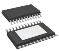
PACKAGE
HTSSOP (24)
BODY SIZE (NOM)
7.80 mm × 4.40 mm
(1) For all available packages, see the orderable addendum at
the end of the data sheet.
Simplified Schematic
VDD: 3.0 V to 5.5 V
SDI
SDI
CLK
CLK
LE
LE
OE
OE
TLC5926/TLC5927-Q1
Controller
OUT0
OUT15
VLED
VDD
SDO
To Controller if Error
Detection Used
R-EXT
GND
1
An IMPORTANT NOTICE at the end of this data sheet addresses availability, warranty, changes, use in safety-critical applications,
intellectual property matters and other important disclaimers. PRODUCTION DATA.
�TLC5926-Q1, TLC5927-Q1
SLVS973A – SEPTEMBER 2009 – REVISED JULY 2015
www.ti.com
Table of Contents
1
2
3
4
5
6
7
8
9
Features ..................................................................
Applications ...........................................................
Description .............................................................
Revision History.....................................................
Device Comparison Table.....................................
Pin Configuration and Functions .........................
Specifications.........................................................
1
1
1
2
3
3
4
7.1
7.2
7.3
7.4
7.5
7.6
7.7
7.8
7.9
7.10
4
4
4
5
5
6
7
8
9
9
Absolute Maximum Ratings .....................................
ESD Ratings..............................................................
Recommended Operating Conditions.......................
Thermal Information ..................................................
Electrical Characteristics: VDD = 3 V.........................
Electrical Characteristics: VDD = 5.5 V......................
Timing Requirements ................................................
Switching Characteristics: VDD = 3 V........................
Switching Characteristics: VDD = 5.5 V.....................
Typical Characteristics ............................................
Parameter Measurement Information ................ 10
Detailed Description ............................................ 13
9.1
9.2
9.3
9.4
Overview .................................................................
Functional Block Diagram .......................................
Feature Description.................................................
Device Functional Modes........................................
13
13
14
15
10 Application and Implementation........................ 20
10.1 Application Information.......................................... 20
10.2 Typical Applications .............................................. 22
11 Power Supply Recommendations ..................... 26
12 Layout................................................................... 26
12.1 Layout Guidelines ................................................. 26
12.2 Layout Example .................................................... 27
13 Device and Documentation Support ................. 28
13.1
13.2
13.3
13.4
13.5
Related Links ........................................................
Community Resources..........................................
Trademarks ...........................................................
Electrostatic Discharge Caution ............................
Glossary ................................................................
28
28
28
28
28
14 Mechanical, Packaging, and Orderable
Information ........................................................... 28
4 Revision History
NOTE: Page numbers for previous revisions may differ from page numbers in the current version.
Changes from Original (September 2009) to Revision A
Page
•
Added Pin Configuration and Functions section, ESD Ratings table, Feature Description section, Device Functional
Modes, Application and Implementation section, Power Supply Recommendations section, Layout section, Device
and Documentation Support section, and Mechanical, Packaging, and Orderable Information section .............................. 1
•
Corrected table title from "8-Bit" to "16-Bit" ......................................................................................................................... 20
2
Submit Documentation Feedback
Copyright © 2009–2015, Texas Instruments Incorporated
Product Folder Links: TLC5926-Q1 TLC5927-Q1
�TLC5926-Q1, TLC5927-Q1
www.ti.com
SLVS973A – SEPTEMBER 2009 – REVISED JULY 2015
5 Device Comparison Table
(1)
DEVICE (1)
OPEN-LOAD
DETECTION
SHORT TO GND
DETECTION
TLC5926-Q1
x
x
TLC5927-Q1
x
x
SHORT TO VLED
DETECTION
x
The device has one single error register for all these conditions (one error bit per channel)
6 Pin Configuration and Functions
PWP Package
24-Pin HTSSOP With PowerPAD™
Top View
GND
SDI
CLK
LE(ED1)
OUT0
OUT1
OUT2
OUT3
OUT4
OUT5
OUT6
OUT7
1
24
2
23
3
22
4
5
21
20
6
19
7
18
8
17
9
16
10
15
11
14
12
13
VDD
R-EXT
SDO
OE(ED2)
OUT15
OUT14
OUT13
OUT12
OUT11
OUT10
OUT9
OUT8
NOTE: The exposed thermal pad should be connected to ground in all applications.
Pin Functions
PIN
NAME
NO.
I/O
DESCRIPTION
CLK
3
I
Clock input for data shift on rising edge
GND
1
—
Ground for control logic and current sink
LE(ED1)
4
I
Data strobe input
Serial data is transferred to the respective latch when LE(ED1) is high. The data is latched when
LE(ED1) goes low. Also, a control signal input for an Error Detection mode and Current Adjust mode
(See Timing Diagram). LE(ED1) has an internal pulldown.
OE(ED2)
21
I
Output enable. When OE (ED2)(active) is low, the output drivers are enabled; when OE(ED2) is high, all
output drivers are turned OFF (blanked). Also, a control signal input for an Error Detection mode and
Current Adjust mode (See Device Functional Modes). OE(ED2) has an internal pullup.
15, 16,
17, 18,
19, 20
O
Constant-current output
23
I
Input pin used to connect an external resistor for setting up all output currents
OUT0–OUT
15
R-EXT
SDI
2
I
Serial-data input to the Shift register
SDO
22
O
Serial-data output to the following SDI of next driver IC or to the microcontroller
VDD
24
I
Supply voltage
Exposed
Thermal PAD (1)
(1)
—
Connect to GND. The thermal pad should be soldered to ground in all applications.
The exposed Thermal PAD should be connected to ground in all applications.
Copyright © 2009–2015, Texas Instruments Incorporated
Product Folder Links: TLC5926-Q1 TLC5927-Q1
Submit Documentation Feedback
3
�TLC5926-Q1, TLC5927-Q1
SLVS973A – SEPTEMBER 2009 – REVISED JULY 2015
www.ti.com
7 Specifications
7.1 Absolute Maximum Ratings
over operating free-air temperature range (unless otherwise noted) (1)
(2) (3) (4)
VDD
VI
(2) (5)
VO
(2) (6) (7)
MIN
MAX
UNIT
0
7
V
Input voltage
–0.4
VDD + 0.4
V
Output voltage
–0.5
20
V
120
mA
Supply voltage
IOUT
Output current
IGND
GND terminal current
1920
mA
TA
Free-air operating temperature
–40
125
°C
TJ
Operating junction temperature
–40
150
°C
Tstg
Storage temperature
–55
150
°C
(1)
(2)
(3)
(4)
(5)
(6)
(7)
Stresses beyond those listed under Absolute Maximum Ratings may cause permanent damage to the device. These are stress ratings
only, and functional operation of the device at these or any other conditions beyond those indicated under Recommended Operating
Conditions is not implied. Exposure to absolute-maximum-rated conditions for extended periods may affect device reliability.
All voltage values are with respect to GND.
Absolute negative voltage on these terminals not to go below 0 V
Absolute maximum voltage 7 V for 200 ms
Absolute negative voltage on these terminals not to go below –0.4 V
Absolute negative voltage on these terminals not to go below –0.5 V
Absolute maximum voltage 20 V for 200 ms
7.2 ESD Ratings
V(ESD)
(1)
Electrostatic discharge
Human body model (HBM), per AEC Q100-002 (1)
VALUE
UNIT
±2000
V
AEC Q100-002 indicates HBM stressing is done in accordance with the ANSI/ESDA/JEDEC JS-001 specification.
7.3 Recommended Operating Conditions
over operating free-air temperature range (unless otherwise noted)
MIN
MAX
3
5.5
UNIT
V
17
V
VDD
Supply voltage
VO
Supply voltage to the output pins
OUT0–OUT15
IO
Output current
DC test circuit
IOH
High-level output current
SDO shorted to GND
IOL
Low-level output current
SDO shorted to GND
VIH
High-level input voltage
CLK, OE(ED2), LE(ED1), and SDI
0.7 × VDD
VDD
V
VIL
Low-level input voltage
CLK, OE(ED2), LE(ED1), and SDI
0
0.3 × VDD
V
4
Submit Documentation Feedback
VO ≥ 0.6 V
5
VO ≥ 1 V
120
mA
–1
mA
1
mA
Copyright © 2009–2015, Texas Instruments Incorporated
Product Folder Links: TLC5926-Q1 TLC5927-Q1
�TLC5926-Q1, TLC5927-Q1
www.ti.com
SLVS973A – SEPTEMBER 2009 – REVISED JULY 2015
7.4 Thermal Information
TLC592x-Q1
THERMAL METRIC (1) (2)
PWP (HTSSOP)
UNIT
24 PINS
Junction-to-ambient
thermal resistance
RθJA
Mounted on JEDEC 1-layer board (JESD 51-3), No airflow
63.9
Mounted on JEDEC 4-layer board (JESD 51-7), No airflow
42.7
Mounted on JEDEC 4-layer board (JESD 51-5), No airflow
39.7
°C/W
RθJC(top)
Junction-to-case (top) thermal resistance
23.4
°C/W
RθJB
Junction-to-board thermal resistance
20.4
°C/W
ψJT
Junction-to-top characterization parameter
0.7
°C/W
ψJB
Junction-to-board characterization parameter
20.2
°C/W
RθJC(bot)
Junction-to-case (bottom) thermal resistance
3.9
°C/W
(1)
(2)
For more information about traditional and new thermal metrics, see the Semiconductor and IC Package Thermal Metrics application
report, SPRA953.
The thermal data is based on JEDEC standard high-K profile – JESD 51-5. The copper pad is soldered to the thermal land pattern. Also,
correct attachment procedure must be incorporated.
7.5 Electrical Characteristics: VDD = 3 V
VDD = 3 V, TJ = –40°C to 125°C (unless otherwise noted)
PARAMETER
TEST CONDITIONS
MIN
TYP
MAX
VO
Supply voltage to the
output pins
IO
Output current
VIH
High-level input voltage
0.7 ×
VDD
VDD
VIL
Low-level input voltage
GND
0.3 × VDD
17
VO ≥ 0.6 V
TLC5926-Q1, VOH = 17 V
Ileak
5
VO ≥ 1 V
Output leakage current
TLC5927-Q1, VOH = 17 V
120
TJ = 25°C
Low-level output voltage
SDO, IOH = 1 mA
Output current 1
VOUT = 0.6 V, Rext = 720 Ω, CG = 0.992
IO (1)
(2)
(2)
0.4
26
±6%
Output current 2
VO = 0.8 V, Rext = 360 Ω, CG = 0.992
52%
V
mA
Output current error, die- IOL = 52 mA, VO = 0.8 V, Rext = 360 Ω, TJ =
to-die
25°C
±6%
IOL = 52 mA, VO = 0.8 V, Rext = 360 Ω, TJ =
25°C
±6%
Output current vs supply
VDD = 3 V to 5.5 V, IO = 26 mA/120 mA
voltage
μA
mA
IOL = 26 mA, VO = 0.6 V, Rext = 720 Ω, TJ =
25°C
IOUT vs VDD
V
V
Output current error,
channel-to-channel
Output current vs
VO = 1 V to 3 V, IO = 26 mA
output voltage regulation
(2)
VDD –
0.4
±6%
IOUT vs VOUT
mA
5
Output current error, die- IOL = 26 mA, VO = 0.6 V, Rext = 720 Ω, TJ =
to-die
25°C
Output current error,
channel-to-channel
(1)
0.5
TJ = 125°C
VOL
IO (1)
1
TJ = 25°C
High-level output voltage SDO, IOL = –1 mA
V
0.5
TJ = 125°C
VOH
UNIT
±0.1
%/V
±1
Pullup resistance
OE(ED2)
250
500
800
kΩ
Pulldown resistance
LE(ED1)
250
500
800
kΩ
Typical values represent the likely parametric nominal values determined at the time of characterization. Typical values depend on the
application and configuration and may vary over time. Typical values are not ensured on production material.
Specified by design
Copyright © 2009–2015, Texas Instruments Incorporated
Product Folder Links: TLC5926-Q1 TLC5927-Q1
Submit Documentation Feedback
5
�TLC5926-Q1, TLC5927-Q1
SLVS973A – SEPTEMBER 2009 – REVISED JULY 2015
www.ti.com
Electrical Characteristics: VDD = 3 V (continued)
VDD = 3 V, TJ = –40°C to 125°C (unless otherwise noted)
PARAMETER
TEST CONDITIONS
MIN
TYP
MAX
UNIT
150
175
200
°C
Tsd
Overtemperature
shutdown (2)
Thys
Restart temperature
hysteresis
IOUT,Th
Threshold current for
open error detection
IOUT,target = 5 mA to 120 mA
VOUT,TTh
Trigger threshold
voltage for short-error
detection
(TLC5927 only)
IOUT,target = 5 mA to 120 mA
2.3
VOUT, RTh
Return threshold voltage
for short-error detection IOUT,target = 5 mA to 120 mA
(TLC5927 only)
1.9
IDD
Supply current
15
°C
0.5 × Itarget%
2.6
3.2
V
V
OUT0–OUT15 = off, Rext = Open, OE = VIH
10
OUT0–OUT15 = off, Rext = 720 Ω, OE = VIH
14
OUT0–OUT15 = off, Rext = 360 Ω, OE = VIH
18
OUT0–OUT15 = off, Rext = 180 Ω, OE = VIH
20
OUT0–OUT15 = on, Rext = 720 Ω, OE = VIL
14
OUT0–OUT15 = on, Rext = 360 Ω, OE = VIL
18
OUT0–OUT15 = on, Rext = 180 Ω, OE = VIL
20
mA
7.6 Electrical Characteristics: VDD = 5.5 V
VDD = 5.5 V, TJ = –40°C to 125°C (unless otherwise noted)
PARAMETER
TEST CONDITIONS
MIN
TYP
MAX
VO
Supply voltage to the
output pins
IO
Output current
VIH
High-level input voltage
0.7 × VDD
VDD
VIL
Low-level input voltage
GND
0.3 × VDD
17
VO ≥ 0.6 V
VO ≥ 1 V
TLC5926, VOH = 17 V
Ileak
5
Output leakage current
TLC5927, VOH = 17 V
120
TJ = 25°C
Low-level output voltage
SDO, IOH = 1 mA
Output current 1
VOUT = 0.6 V, Rext = 720 Ω, CG = 0.992
IO(2)
(1)
(2)
6
(1) (1)
(1) (2)
0.5
TJ = 125°C
High-level output voltage SDO, IOL = –1 mA
IO(1)
1
TJ = 25°C
VOL
V
mA
V
0.5
TJ = 125°C
VOH
UNIT
5
VDD – 0.4
V
0.4
26
V
mA
Output current error, dieIOL = 26 mA, VO = 0.6 V, Rext = 720 Ω, TJ = 25°C
to-die
±6%
Output current error,
channel-to-channel
IOL = 26 mA, VO = 0.6 V, Rext = 720 Ω, TJ = 25°C
±6%
Output current 2
VO = 0.8 V, Rext = 360 Ω, CG = 0.992
52
mA
Output current error, dieIOL = 52 mA, VO = 0.8 V, Rext = 360 Ω, TJ = 25°C
to-die
±6%
Output current error,
channel-to-channel
±6%
IOL = 52 mA, VO = 0.8 V, Rext = 360 Ω, TJ = 25°C
μA
Typical values represent the likely parametric nominal values determined at the time of characterization. Typical values depend on the
application and configuration and may vary over time. Typical values are not ensured on production material.
Specified by design
Submit Documentation Feedback
Copyright © 2009–2015, Texas Instruments Incorporated
Product Folder Links: TLC5926-Q1 TLC5927-Q1
�TLC5926-Q1, TLC5927-Q1
www.ti.com
SLVS973A – SEPTEMBER 2009 – REVISED JULY 2015
Electrical Characteristics: VDD = 5.5 V (continued)
VDD = 5.5 V, TJ = –40°C to 125°C (unless otherwise noted)
PARAMETER
TEST CONDITIONS
MIN
TYP
MAX
UNIT
IOUT vs VOUT
Output current vs
VO = 1 V to 3 V, IO = 26 mA
output voltage regulation
IOUT vs VDD
Output current vs supply
voltage
VDD = 3 V to 5.5 V, IO = 26 mA/120 mA
Pullup resistance
OE(ED2)
250
500
800
kΩ
Pulldown resistance
LE(ED1)
250
500
800
kΩ
150
175
200
°C
±0.1
%/V
±1
Tsd
Overtemperature
shutdown (2)
Thys
Restart temperature
hysteresis
IOUT,Th
Threshold current for
open error detection
VOUT,TTh
Trigger threshold voltage
for short-error detection IOUT,target = 5 mA to 120 mA
(TLC5927 only)
2.3
VOUT, RTh
Return threshold voltage
for short-error detection
(TLC5927 only)
1.9
IDD
Supply current
15
0.5 ×
Itarget
%
IOUT,target = 5 mA to 120 mA
IOUT,target = 5 mA to 120 mA
°C
2.6
3.2
V
V
OUT0–OUT15 = off, Rext = Open, OE = VIH
11
OUT0–OUT15 = off, Rext = 720 Ω, OE = VIH
17
OUT0–OUT15 = off, Rext = 360 Ω, OE = VIH
18
OUT0–OUT15 = off, Rext = 180 Ω, OE = VIH
25
OUT0–OUT15 = on, Rext = 720 Ω, OE = VIL
17
OUT0–OUT15 = on, Rext = 360 Ω, OE = VIL
18
OUT0–OUT15 = on, Rext = 180 Ω, OE = VIL
25
mA
7.7 Timing Requirements
VDD = 3 V to 5.5 V (unless otherwise noted)
MIN
tw(L)
LE(ED1) pulse duration
Normal mode
tw(CLK)
CLK pulse duration
tw(OE)
OE(ED2) pulse duration
tsu(D)
MAX
UNIT
20
ns
Normal mode
20
ns
Normal mode
1000
ns
Setup time for SDI
Normal mode
7
ns
th(D)
Hold time for SDI
Normal mode
3
ns
tsu(L)
Setup time for LE(ED1)
Normal mode
18
ns
th(L)
Hold time for LE(ED1)
Normal mode
18
ns
tw(CLK)
CLK pulse duration
Error Detection mode
20
ns
tw(ED2)
OE(ED2) pulse duration
Error Detection mode
2000
ns
tsu(ED1)
Setup time for LE(ED1)
Error Detection mode
7
ns
th(ED1)
Hold time for LE(ED1)
Error Detection mode
10
ns
tsu(ED2)
Setup time for OE(ED2)
Error Detection mode
7
ns
th(ED2)
Hold time for OE(ED2)
Error Detection mode
10
fCLK
Clock frequency
Cascade operation, VDD = 3 V to 5.5 V
Copyright © 2009–2015, Texas Instruments Incorporated
Product Folder Links: TLC5926-Q1 TLC5927-Q1
ns
30
Submit Documentation Feedback
MHz
7
�TLC5926-Q1, TLC5927-Q1
SLVS973A – SEPTEMBER 2009 – REVISED JULY 2015
www.ti.com
7.8 Switching Characteristics: VDD = 3 V
VDD = 3 V, TJ = –40°C to 125°C (unless otherwise noted)
PARAMETER
TEST CONDITIONS
MIN
TYP
MAX
UNIT
tPLH1
Low-to-high propagation delay time, CLK to OUTn
35
65
105
ns
tPLH2
Low-to-high propagation delay time, LE(ED1) to OUTn
35
65
105
ns
tPLH3
Low-to-high propagation delay time, OE(ED2) to OUTn
35
65
105
ns
tPLH4
Low-to-high propagation delay time, CLK to SDO
20
45
ns
tPHL1
High-to-low propagation delay time, CLK to OUTn
200
300
470
ns
tPHL2
High-to-low propagation delay time, LE(ED1) to OUTn
200
300
470
ns
tPHL3
High-to-low propagation delay time, OE(ED2) to OUTn
200
300
470
ns
tPHL4
High-to-low propagation delay time, CLK to SDO
20
40
ns
tw(CLK)
Pulse duration, CLK
tw(L)
Pulse duration LE(ED1)
tw(OE)
Pulse duration, OE(ED2)
tw(ED2)
Pulse duration, OE(ED2) in Error Detection mode
th(ED1,ED2)
Hold time, LE(ED1), and OE(ED2)
th(D)
Hold time, SDI
tsu(D,ED1,ED2)
Setup time, SDI, LE(ED1), and OE(ED2)
th(L)
Hold time, LE(ED1), Normal mode
tsu(L)
Setup time, LE(ED1), Normal mode
18
ns
VIH = VDD, VIL = GND,
Rext = 360 Ω, VL = 4 V,
RL = 44 Ω, CL = 70 pF,
CG = 0.992
(1)
20
ns
20
ns
1000
ns
2
μs
10
ns
5
ns
7
ns
18
ns
tr
Rise time, CLK
500
ns
tf
Fall time, CLK (1)
500
ns
tor
Rise time, outputs (off)
245
ns
tof
Rise time, outputs (on)
fCLK
Clock frequency
(1)
8
Cascade operation
600
ns
30
MHz
If the devices are connected in cascade and tr or tf is large, it may be critical to achieve the timing required for data transfer between two
cascaded devices.
Submit Documentation Feedback
Copyright © 2009–2015, Texas Instruments Incorporated
Product Folder Links: TLC5926-Q1 TLC5927-Q1
�TLC5926-Q1, TLC5927-Q1
www.ti.com
SLVS973A – SEPTEMBER 2009 – REVISED JULY 2015
7.9 Switching Characteristics: VDD = 5.5 V
VDD = 5.5 V, TJ = –40°C to 125°C (unless otherwise noted)
PARAMETER
TEST CONDITIONS
MIN
TYP
MAX
UNIT
tPLH1
Low-to-high propagation delay time, CLK to OUTn
27
65
95
ns
tPLH2
Low-to-high propagation delay time, LE(ED1) to OUTn
27
65
95
ns
tPLH3
Low-to-high propagation delay time, OE(ED2) to OUTn
27
65
95
ns
tPLH4
Low-to-high propagation delay time, CLK to SDO
20
30
ns
tPHL1
High-to-low propagation delay time, CLK to OUTn
180
300
445
ns
tPHL2
High-to-low propagation delay time, LE(ED1) to OUTn
180
300
445
ns
tPHL3
High-to-low propagation delay time, OE(ED2) to OUTn
180
300
445
ns
tPHL4
High-to-low propagation delay time, CLK to SDO
20
30
ns
tw(CLK)
Pulse duration, CLK
tw(L)
Pulse duration LE(ED1)
tw(OE)
Pulse duration, OE(ED2)
tw(ED2)
Pulse duration, OE(ED2) in Error Detection mode
th(ED1,ED2)
Hold time, LE(ED1), and OE(ED2)
th(D)
Hold time, SDI
tsu(D,ED1,ED2)
Setup time, SDI, LE(ED1), and OE(ED2)
th(L)
Hold time, LE(ED1), Normal mode
tsu(L)
Setup time, LE(ED1), Normal mode
15
ns
VIH = VDD, VIL = GND,
Rext = 360 Ω, VL = 4 V,
RL = 44 Ω, CL = 70 pF,
CG = 0.992
20
ns
20
ns
1000
ns
2
μs
10
ns
3
ns
4
ns
15
ns
(1)
tr
Rise time, CLK
500
ns
tf
Fall time, CLK (1)
500
ns
tor
Rise time, outputs (off)
245
ns
tof
Rise time, outputs (on)
fCLK
Clock frequency
(1)
Cascade operation
570
ns
30
MHz
If the devices are connected in cascade and tr or tf is large, it may be critical to achieve the timing required for data transfer between two
cascaded devices.
7.10 Typical Characteristics
Figure 1: At low voltage levels (VO), the output current (IO) may be limited. Figure 1 shows the dependency of the output
current on the output voltage.
150
Temperature = 25°C
IO = 120 mA
125
IO – Output Current – mA
IO = 100 mA
100
IO = 80 mA
75
IO = 60 mA
50
IO = 40 mA
IO = 20 mA
25
IO = 5 mA
0
0
0.5
1
1.5
2
2.5
3
VO – Output Voltage – V
Figure 1. Output Current vs Output Voltage
Copyright © 2009–2015, Texas Instruments Incorporated
Product Folder Links: TLC5926-Q1 TLC5927-Q1
Submit Documentation Feedback
9
�TLC5926-Q1, TLC5927-Q1
SLVS973A – SEPTEMBER 2009 – REVISED JULY 2015
www.ti.com
8 Parameter Measurement Information
IDD
VDD
OE(ED2)
IIH, IIL
IOUT
OUT0
CLK
LE(ED1)
OUT15
SDI
VIH, VIL
R-EXT
GND
SDO
Iref
Figure 2. Test Circuit for Electrical Characteristics
IDD
IOUT
VDD
VIH, VIL
OE(ED2)
CLK
LE(ED1)
Function
Generator
OUT0
OUT15
RL
CL
SDI
Logic input
waveform
VIH = VDD
VIL = 0V
R-EXT
Iref
GND
SDO
CL
VL
Figure 3. Test Circuit for Switching Characteristics
10
Submit Documentation Feedback
Copyright © 2009–2015, Texas Instruments Incorporated
Product Folder Links: TLC5926-Q1 TLC5927-Q1
�TLC5926-Q1, TLC5927-Q1
www.ti.com
SLVS973A – SEPTEMBER 2009 – REVISED JULY 2015
Parameter Measurement Information (continued)
tw(CLK)
CLK
50%
tsu(D)
SDI
50%
50%
th(D)
50%
50%
tPLH4, tPHL4
50%
SDO
tw(L)
50%
LE(ED1)
tsu(L)
th(L)
OE Low
OE(ED2)
LOW
tPLH2, tPHL2
Output off
OUTn
50%
Output on
tPLH1, tPHL1
tw(OE)
HIGH
50%
OE Pulsed
OE(ED2)
50%
tPLH3
tPHL3
Output off
90%
OUTn
90%
50%
50%
10%
tof
10%
tor
Figure 4. Normal Mode Timing Waveforms
Copyright © 2009–2015, Texas Instruments Incorporated
Product Folder Links: TLC5926-Q1 TLC5927-Q1
Submit Documentation Feedback
11
�TLC5926-Q1, TLC5927-Q1
SLVS973A – SEPTEMBER 2009 – REVISED JULY 2015
www.ti.com
Parameter Measurement Information (continued)
tw(CLK)
50%
CLK
tsu(ED2)
OE(ED2)
th(ED2)
50%
tsu(ED1)
LE(ED1)
th(ED1)
50%
2 CLK
Figure 5. Switching to Special Mode Timing Waveforms
CLK
OE(ED2)
50%
50%
tw(ED2)
Figure 6. Reading Error Status Code Timing Waveforms
12
Submit Documentation Feedback
Copyright © 2009–2015, Texas Instruments Incorporated
Product Folder Links: TLC5926-Q1 TLC5927-Q1
�TLC5926-Q1, TLC5927-Q1
www.ti.com
SLVS973A – SEPTEMBER 2009 – REVISED JULY 2015
9 Detailed Description
9.1 Overview
The TLC592x-Q1 is designed for LED displays and LED lighting applications with open-load, shorted-load, and
overtemperature detection, and constant-current control. The TLC592x-Q1 contains a 16-bit shift register and
data latches, which convert serial input data into parallel output format. At the TLC592x-Q1 output stage, 16
regulated- current ports provide uniform and constant current for driving LEDs within a wide range of VF
(Forward Voltage) variations. Used in systems designed for LED display applications (that is, LED panels),
TLC592x-Q1 provides great flexibility and device performance. Users can adjust the output current from 5 mA to
120 mA through an external resistor, R-EXT, which gives flexibility in controlling the light intensity of LEDs.
TLC592x-Q1 is designed for up to 17 V at the output port. The high clock frequency, 30 MHz, also satisfies the
system requirements of high-volume data transmission.
9.2 Functional Block Diagram
OUT0
R-EXT
OUT1
OUT14
OUT15
I/O REGULATOR
VDD
16
OUTPUT DRIVER and
ERROR DETECTION
OE(ED2)
CONTROL
LOGIC
16
16
16-BIT OUTPUT
LATCH
LE(ED1)
CONFIGURATION
LATCHES
16
CLK
16
16-BIT SHIFT
REGISTER
SDI
SDO
16
Copyright © 2009–2015, Texas Instruments Incorporated
Product Folder Links: TLC5926-Q1 TLC5927-Q1
Submit Documentation Feedback
13
�TLC5926-Q1, TLC5927-Q1
SLVS973A – SEPTEMBER 2009 – REVISED JULY 2015
www.ti.com
9.3 Feature Description
9.3.1 Open-Circuit Detection Principle
The LED Open-Circuit Detection compares the effective current level IOUT with the open load detection threshold
current IOUT,Th. If IOUT is below the IOUT,Th threshold, the TLC592x-Q1 detects an open-load condition. This error
status can be read as an error status code in the Special mode. For open-circuit error detection, a channel must
be on.
Table 1. Open-Circuit Detection
STATE OF OUTPUT PORT
Off
On
(1)
CONDITION OF
OUTPUT CURRENT
ERROR STATUS CODE
MEANING
IOUT = 0 mA
0
Detection not possible
IOUT < IOUT,Th
(1)
0
Open circuit
IOUT ≥ IOUT,Th
(1)
1
Normal
IOUT,Th = 0.5 × IOUT,target (typical)
9.3.2 Short-Circuit Detection Principle (TLC5927-Q1 Only)
The LED short-circuit detection compares the effective voltage level VOUT with the shorted-load detection
threshold voltages VOUT,TTh and VOUT,RTh. If VOUT is above the VOUT,TTh threshold, the TLC5927-Q1 detects a
shorted-load condition. If the VOUT is below VOUT,RTh threshold, no error is detected and the error bit is reset. This
error status can be read as an error status code in the Special mode. For short-circuit error detection, a channel
must be on.
Table 2. Short-Circuit Detection
STATE OF OUTPUT PORT
Off
On
CONDITION OF
OUTPUT VOLTAGE
ERROR STATUS CODE
MEANING
IOUT = 0 mA
0
Detection not possible
VOUT ≥ VOUT,TTh
0
Short circuit
VOUT < VOUT,RTh
1
Normal
Minimum
Return
Threshold
Minimum
Trigger
Threshold
1.9 V
VOUT,RTh
2.3 V
Maximum
Trigger
Threshold
No Fault
Short Fault
3.2 V
VOUT,TTh
VOUT
Figure 7. Short-Circuit Detection Principle
14
Submit Documentation Feedback
Copyright © 2009–2015, Texas Instruments Incorporated
Product Folder Links: TLC5926-Q1 TLC5927-Q1
�TLC5926-Q1, TLC5927-Q1
www.ti.com
SLVS973A – SEPTEMBER 2009 – REVISED JULY 2015
9.3.3 Overtemperature Detection and Shutdown
The TLC592x-Q1 is equipped with a global overtemperature sensor and 16 individual, channel-specific
overtemperature sensors.
• When the global sensor reaches the trip temperature, all output channels are shutdown, and the error status
is stored in the internal Error Status register of every channel. After shutdown, the channels automatically
restart after cooling down, if the control signal (output latch) remains on. The stored error status is not reset
after cooling down and can be read out as the error status code in the Special mode.
• When one of the channel-specific sensors reaches trip temperature, only the affected output channel is shut
down, and the error status is stored only in the internal Error Status register of the affected channel. After
shutdown, the channel automatically restarts after cooling down, if the control signal (output latch) remains
on. The stored error status is not reset after cooling down and can be read out as error status code in the
Special mode.
For channel-specific overtemperature error detection, a channel must be on.
The error status code is reset when the TLC592x-Q1 returns to Normal mode.
Table 3. Overtemperature Detection (1)
(1)
STATE OF OUTPUT PORT
CONDITION
ERROR STATUS CODE
Off
IOUT = 0 mA
0
MEANING
On
On → all channels
Off
Tj < Tj,trip global
1
Normal
Tj > Tj,trip global
All error status bits = 0
Global overtemperature
On
On → Off
Tj < Tj,trip channel n
1
Normal
Tj > Tj,trip channel n
Channel n error status bit = 0
Channel n overtemperature
The global shutdown threshold temperature is approximately 170°C.
9.4 Device Functional Modes
The TLC5926/TLC5927-Q1 provides a Special Mode in which two functions are included: Error Detection and
Current Gain Control. In the TLC5926/TLC5927-Q1 there are two operation modes and three phases: Normal
Mode phase, Mode Switching transition phase, and Special mode phase. The signal on the multiple- function pin
OE(ED2) is monitored, and when a one- clock-wide short pulse appears on OE(ED2), TLC5926/TLC5927-Q1
enters the Mode Switching phase. At this time, the voltage level on LE (ED1) determines the next mode into
which the TLC5926/TLC5927-Q1 switches.
In the Normal Mode phase, the serial data is transferred into TLC5926/TLC5927-Q1 via SDI, shifted in the shift
register, and transferred out via SDO. LE (ED1) can latch the serial data in the shift register to the output latch.
OE(ED2) enables the output drivers to sink current.
In the Special Mode phase, the low-voltage-level signal OE(ED2) can enable output channels and detect the
status of the output current, to tell if the driving current level is enough or not. The detected error status is loaded
into the 16-bit shift register and shifted out via SDO, along with the CLK signal. The system controller can read
the error status to determine whether or not the LEDs are properly lit. In the Special Mode phase,
TLC5926/TLC5927-Q1 also allows users to adjust the output current level by setting a runtime-programmable
Configuration Code. The code is sent into TLC5926/TLC5927-Q1 via SDI. The positive pulse of LE (ED1) latches
the code in the shift register into a built-in 8-bit configuration latch, instead of the output latch. The code affects
the voltage at R-EXT and controls the output-current regulator. The output current can be adjusted finely by a
gain ranging from 1/12 to 127/128 in 256 steps. Therefore, the current skew between ICs can be compensated
within less than 1%, and this feature is suitable for white balancing in LED color-display panels.
Copyright © 2009–2015, Texas Instruments Incorporated
Product Folder Links: TLC5926-Q1 TLC5927-Q1
Submit Documentation Feedback
15
�TLC5926-Q1, TLC5927-Q1
SLVS973A – SEPTEMBER 2009 – REVISED JULY 2015
www.ti.com
Device Functional Modes (continued)
0
1
2
3
4
5
6
7
8
9 10 11 12 13 14 15
CLK
OE(ED2)
1
LE(ED1)
0
SDI
off
OUT0
on
off
OUT1
on
off
OUT2
on
off
OUT3
on
off
OUT15
on
SDO
Don't care
Figure 8. Normal Mode
Table 4. Truth Table in Normal Mode
CLK
LE(ED1)
OE(ED2)
SDI
OUT0...OUT15
SDO
↑
H
L
Dn
Dn...Dn – 7...Dn – 15
Dn – 15
↑
L
L
Dn + 1
No change
Dn – 14
↑
H
L
Dn + 2
Dn + 2...Dn – 5...Dn – 13
Dn – 13
↓
X
L
Dn + 3
Dn + 2...Dn – 5...Dn – 13
Dn – 13
↓
X
H
Dn + 3
off
Dn – 13
The signal sequence shown in Figure 9 makes the TLC592x-Q1 enter Current Adjust and Error Detection mode.
1
2
3
4
5
OE(ED2)
1
0
1
1
1
LE(ED1)
0
0
0
1
0
CLK
Figure 9. Switching to Special Mode
16
Submit Documentation Feedback
Copyright © 2009–2015, Texas Instruments Incorporated
Product Folder Links: TLC5926-Q1 TLC5927-Q1
�TLC5926-Q1, TLC5927-Q1
www.ti.com
SLVS973A – SEPTEMBER 2009 – REVISED JULY 2015
In the Current Adjust mode, sending the positive pulse of LE(ED1), the content of the shift register (a current
adjust code) is written to the 16-bit configuration latch (see Figure 10).
0
1
2
3
14
15
CLK
OE(ED2)
1
LE(ED1)
0
16-bit configuration code
SDI
Figure 10. Writing Configuration Code
When the TLC592x-Q1 is in the error detection mode, the signal sequence shown in Figure 11 enables a system
controller to read error status codes through SDO.
1
2
3
CLK
>2 µs
OE(ED2)
1
LE(ED1)
0
SDO
Error status code
Figure 11. Reading Error Status Code
The signal sequence shown in Figure 12 makes TLC592x-Q1 resume the Normal mode. Switching to Normal
mode resets all internal Error Status registers. OE (ED2) always enables the output port, whether the TLC592xQ1 enters current adjust mode or not.
1
2
3
4
5
OE(ED2)
1
0
1
1
1
LE(ED1)
0
0
0
0
0
CLK
Figure 12. Switching to Normal Mode
Copyright © 2009–2015, Texas Instruments Incorporated
Product Folder Links: TLC5926-Q1 TLC5927-Q1
Submit Documentation Feedback
17
�TLC5926-Q1, TLC5927-Q1
SLVS973A – SEPTEMBER 2009 – REVISED JULY 2015
www.ti.com
9.4.1 Operation Mode Switching
In order to switch between its two modes, TLC592x-Q1 monitors the signal OE(ED2). When a one-clock-wide
pulse of OE(ED2) appears, TLC592x-Q1 enters the two-clock-period transition phase, the Mode Switching
phase. After power on, the default operation mode is the Normal Mode (see Figure 13).
Switching to Special Mode
1
2
3
Switching to Normal Mode
4
5
1
CLK
2
3
4
5
CLK
OE(ED2)
1
0
1
1
1
OE(ED2)
1
0
1
1
1
LE(ED1)
0
0
0
1
0
LE(ED1)
0
0
0
0
0
Actual Mode
Phase (Normal or Special)
Mode
Switching
Special
Mode
Actual Mode
Phase (Normal or Special)
Mode
Switching
Normal
Mode
Figure 13. Mode Switching
As shown in Figure 13, once a one-clock-wide short pulse (101) of OE(ED2) appears, TLC592x-Q1 enters the
Mode Switching phase. At the fourth rising edge of CLK, if LE(ED1) is sampled as voltage high, TLC592x-Q1
switches to Special mode; otherwise, it switches to Normal mode. The signal LE(ED1) between the third and the
fifth rising edges of CLK cannot latch any data. Its level is used only to determine into which mode to switch.
However, the short pulse of OE(ED2) can still enable the output ports. During mode switching, the serial data
can still be transferred through SDI and shifted out from SDO.
NOTE
1. The signal sequence for the mode switching may be used frequently to ensure that
the TLC592x-Q1 is in the proper mode.
2. The 1 and 0 on the LE(ED1) signal are sampled at the rising edge of CLK. The X
means its level does not affect the result of mode switching mechanism.
3. After power on, the default operation mode is Normal mode.
9.4.2 Normal Mode Phase
Serial data is transferred into TLC592x-Q1 via SDI, shifted in the Shift Register, and output via SDO. LE(ED1)
can latch the serial data in the Shift Register to the Output Latch. OE(ED2) enables the output drivers to sink
current. These functions differ only as described in Operation Mode Switching, in which case, a short pulse
triggers TLC592x-Q1 to switch the operation mode. However, as long as LE(ED1) is high in the Mode Switching
phase, TLC592x-Q1 remains in the Normal mode, as if no mode switching occurred.
9.4.3 Special Mode Phase
In the Special mode, as long as OE(ED2) is not low, the serial data is shifted to the Shift Register via SDI and
shifted out via SDO, as in the Normal mode. However, there are two differences between the Special Mode and
the Normal Mode, as shown in the following sections.
9.4.3.1 Reading Error Status Code in Special Mode
When OE(ED2) is pulled low while in Special mode, error detection and load error status codes are loaded into
the Shift Register, in addition to enabling output ports to sink current. Figure 14 shows the timing sequence for
error detection. The 0 and 1 signal levels are sampled at the rising edge of each CLK. At least three zeros must
be sampled at the voltage low signal OE(ED2). Immediately after the second 0 is sampled, the data input source
of the Shift Register changes to the 16-bit parallel Error Status Code register, instead of from the serial data on
SDI. Normally, the error status codes are generated at least 2 μs after the falling edge of OE(ED2). The
18
Submit Documentation Feedback
Copyright © 2009–2015, Texas Instruments Incorporated
Product Folder Links: TLC5926-Q1 TLC5927-Q1
�TLC5926-Q1, TLC5927-Q1
www.ti.com
SLVS973A – SEPTEMBER 2009 – REVISED JULY 2015
occurrence of the third or later 0 saves the detected error status codes into the Shift Register. Therefore, when
OE(ED2) is low, the serial data cannot be shifted into TLC592x-Q1 via SDI. When OE(ED2) is pulled high, the
data input source of the Shift Register is changed back to SDI. At the same time, the output ports are disabled
and the error detection is completed. Then, the error status codes saved in the Shift Register can be shifted out
via SDO bit-by-bit along with CLK, as well as the new serial data can be shifted into TLC592x-Q1 via SDI.
While in Special mode, the TLC592x-Q1 cannot simultaneously transfer serial data and detect LED load error
status.
1
2
3
CLK
>2 µs
OE(ED2)
1
0
0
0
0
0
1
1
1
1
LE(ED1)
0
0
0
0
0
0
0
0
0
0
Error Status Code
SDO
Bit 15 Bit 14 Bit 13 Bit 12
Data source of
shift register
Error Detection
SDI
SDI
Figure 14. Reading Error Status Code
9.4.3.2 Writing Configuration Code in Special Mode
When in Special mode, the active high signal LE(ED1) latches the serial data in the Shift Register to the
Configuration Latch, instead of the Output Latch. The latched serial data is used as the Configuration Code.
The code is stored until power off or the Configuration Latch is rewritten. As shown in Figure 15, the timing for
writing the Configuration Code is the same as the timing in the Normal Mode to latching output channel data.
Both the Configuration Code and Error Status Code are transferred in the common 16-bit Shift Register. Users
must pay attention to the sequence of error detection and current adjustment to avoid the Configuration Code
being overwritten by Error Status Code.
0
1
2
3
4
12
13
14
15
Bit 3
Bit 2
Bit 1
Bit 0
CLK
OE(ED2)
1
LE(ED1)
0
SDI
Bit 15 Bit 14 Bit 13 Bit 12
16-Bit Configuration Code
Figure 15. Writing Configuration Code
Copyright © 2009–2015, Texas Instruments Incorporated
Product Folder Links: TLC5926-Q1 TLC5927-Q1
Submit Documentation Feedback
19
�TLC5926-Q1, TLC5927-Q1
SLVS973A – SEPTEMBER 2009 – REVISED JULY 2015
www.ti.com
10 Application and Implementation
NOTE
Information in the following applications sections is not part of the TI component
specification, and TI does not warrant its accuracy or completeness. TI’s customers are
responsible for determining suitability of components for their purposes. Customers should
validate and test their design implementation to confirm system functionality.
10.1 Application Information
10.1.1 Constant Current
In LED display applications, TLC592x-Q1 provides nearly no current variations from channel to channel and from
IC to IC. While IOUT ≤ 50 mA, the maximum current skew between channels is less than ±6% and between ICs is
less than ±6%.
10.1.2 Adjusting Output Current
TLC592x-Q1 scales up the reference current, Iref, set by the external resistor Rext to sink a current, Iout, at each
output port. Users can follow Equation 1, Equation 2, and Equation 3 to calculate the target output current
IOUT,target in the saturation region:
VR-EXT = 1.26 V × VG
Iref = VR-EXT/Rext, if another end of the external resistor Rext is connected to ground.
IOUT,target = Iref × 15 × 3CM – 1
(1)
(2)
(3)
Where Rext is the resistance of the external resistor connected to the R-EXT terminal, and VR-EXT is the voltage of
R-EXT, which is controlled by the programmable voltage gain (VG), which is defined by the Configuration Code.
The Current Multiplier (CM) determines that the ratio IOUT,target/Iref is 15 or 5. After power on, the default value of
VG is 127/128 = 0.992, and the default value of CM is 1, so that the ratio IOUT,target/Iref = 15. Based on the default
VG and CM.
VR-EXT = 1.26 V × 127 / 128 = 1.25 V
IOUT,target = (1.25 V / Rext) × 15
(4)
(5)
Therefore, the default current is approximately 52 mA at 360 Ω and 26 mA at 720 Ω. The default relationship
after power on between IOUT,target and Rext is shown in Figure 16.
140
IOUT – mA
120
100
80
40
0
0
500
1000 1500 2000 2500 3000 3500 4000
Rext – W
Figure 16. Default Relationship Curve Between IOUT,target and Rext
10.1.3 16-Bit Configuration Code and Current Gain
Table 5 shows the bit definition of the Configuration Code in the Configuration Latch.
Table 5. Bit Definition of 16-Bit Configuration Code
Meaning
Default
20
BIT 0
BIT 1
BIT 2
BIT 3
BIT 4
BIT 5
BIT 6
BIT 7
BIT 15:8
CM
HC
CC0
CC1
CC2
CC3
CC4
CC5
Don't care
1
1
1
1
1
1
1
1
X
Submit Documentation Feedback
Copyright © 2009–2015, Texas Instruments Incorporated
Product Folder Links: TLC5926-Q1 TLC5927-Q1
�TLC5926-Q1, TLC5927-Q1
www.ti.com
SLVS973A – SEPTEMBER 2009 – REVISED JULY 2015
Bit 7 is first sent into TLC592x-Q1 via SDI. Bits 1 to 7 {HC, CC[0:5]} determine the voltage gain (VG) that affects
the voltage at R-EXT and indirectly affects the reference current, Iref, flowing through the external resistor at REXT. Bit 0 is the Current Multiplier (CM) that determines the ratio IOUT,target / Iref. Each combination of VG and CM
gives a specific Current Gain (CG).
• VG: the relationship between {HC,CC[0:5]} and the voltage gain is calculated as:
VG = (1 + HC) × (1 + D/64) / 4
D = CC0 × 25 + CC1 × 24 + CC2 × 23 + CC3 × 22 + CC4 × 21 + CC5 × 20
•
•
(6)
(7)
Where HC is 1 or 0, and D is the binary value of CC[0:5]. So, the VG could be regarded as a floating-point
number with 1-bit exponent HC and 6-bit mantissa CC[0:5]. {HC,CC[0:5]} divides the programmable voltage
gain VG into 128 steps and two sub-bands:
Low voltage sub-band (HC = 0): VG = 1/4 ~ 127/256, linearly divided into 64 steps
High voltage sub-band (HC = 1): VG = 1/2 ~ 127/128, linearly divided into 64 steps
CM: In addition to determining the ratio IOUT,target/Iref, CM limits the output current range.
High Current Multiplier (CM = 1): IOUT,target/Iref = 15, suitable for output current range IOUT = 10 mA to 120 mA.
Low Current Multiplier (CM = 0): IOUT,target/Iref = 5, suitable for output current range IOUT = 5 mA to 40 mA
CG: The total Current Gain is defined as the following.
VR-EXT = 1.26 V × VG
Iref = VR-EXT/Rext, if the external resistor, Rext, is connected to ground.
IOUT,target = Iref × 15 × 3CM – 1 = 1.26 V/Rext × VG × 15 × 3CM – 1 = (1.26 V/Rext × 15) × CG
CG = VG × 3CM – 1
(8)
(9)
(10)
(11)
Therefore, CG = (1/12) to (127/128) divided into 256 steps.
Examples
• Configuration Code {CM, HC, CC[0:5]} = {1,1,111111}
VG = 127/128 = 0.992 and CG = VG × 30 = VG = 0.992
• Configuration Code = {1,1,000000}
VG = (1 + 1) × (1 + 0/64)/4 = 1/2 = 0.5, and CG = 0.5
• Configuration Code = {0,0,000000}
VG = (1 + 0) × (1 + 0/64)/4 = 1/4, and CG = (1/4) × 3–1 = 1/12
After power on, the default value of the Configuration Code {CM, HC, CC[0:5]} is {1,1,111111}. Therefore,
VG = CG = 0.992. The relationship between the Configuration Code and the Current Gain is shown in Figure 17.
1.00
CM = 1 (High Current Multiplier)
CM = 0 (Low Current Multiplier)
Current Gain (CG)
0.75
HC = 0 (Low
Voltage SubBand)
0.50
HC = 1 (High
Voltage SubBand)
HC = 0 (Low
Voltage SubBand)
HC = 1 (High
Voltage SubBand)
0.25
{1,1,110000}
{1,1,100000}
{1,1,010000}
{1,1,000000}
{1,0,110000}
{1,0,100000}
{1,0,010000}
{1,0,000000}
{0,1,110000}
{0,1,100000}
{0,1,010000}
{0,1,000000}
{0,0,110000}
{0,0,100000}
{0,0,010000}
{0,0,000000}
0.00
Configuration Code (CM, HC, CC[0:5]) in Binary Format
Figure 17. Current Gain vs Configuration Code
Copyright © 2009–2015, Texas Instruments Incorporated
Product Folder Links: TLC5926-Q1 TLC5927-Q1
Submit Documentation Feedback
21
�TLC5926-Q1, TLC5927-Q1
SLVS973A – SEPTEMBER 2009 – REVISED JULY 2015
www.ti.com
10.2 Typical Applications
10.2.1 Single Implementation of TLC5926/TLC5927-Q1 Device
The TLC592x-Q1 Constant-Current LED Sink Drivers is designed to work alone or cascaded. shows
implementation of a single TLC591x-Q1 device.
VDD: 3.0 V
to 5.5 V
SDI
SDI
CLK
CLK
LE
LE
OE
OE
TLC5926/TLC5927-Q1
Controller
OUT0
OUT15
VLED
VDD
To Controller if Error
Detection Used
SDO
R-EXT
GND
Figure 18. Simple Implementation of TLC591x-Q1 Circuit
10.2.1.1 Design Requirements
For this design example, use the parameters listed in Table 6. The purpose of this design procedure is to
calculate the power dissipation in the device and the operating junction temperature.
Table 6. Design Parameters
22
DESIGN PARAMETERS
EXAMPLE VALUES
No. of LED strings
16
No. of LEDs per string
3
LED current (mA)
20
Forward voltage of each LED (V)
3.5
Junction-to-ambient thermal resistance (°C/W)
39.7
Ambient temperature of application (°C)
115
VDD (V)
5
IDD (mA)
17
Max operating junction temperature (°C)
150
Submit Documentation Feedback
Copyright © 2009–2015, Texas Instruments Incorporated
Product Folder Links: TLC5926-Q1 TLC5927-Q1
�TLC5926-Q1, TLC5927-Q1
www.ti.com
SLVS973A – SEPTEMBER 2009 – REVISED JULY 2015
10.2.1.2 Detailed Design Procedure
TJ = TA + θJA × PD_TOT
where
•
•
•
•
TJ is the junction temperature
TA is the ambient temperature
θJA is the junction-to-ambient thermal resistance
PD_TOT is the total power dissipation in the IC
(12)
space
PD_TOT = PD_CS + IDD × VDD
where
•
•
•
PD_CS is the power dissipation in the LED current sinks
IDD is the IC supply current
VDD is the IC supply voltage
(13)
space
PD_CS = IO × VO × nCH
where
•
•
•
IO is the LED current
VO is the voltage at the output pin
nCH is the number of LED strings
(14)
space
VO = VLED – (nLED × VF)
where
•
•
•
VLED is the voltage applied to the LED string
nLED is the number of LEDs in the string
VF is the forward voltage of each LED
(15)
space
VO must not be too high as this will cause excess power dissipation inside the current sink. However, VO must
also not be too low as this will not allow the full LED current (refer to the output voltage vs. output current graph).
With VLED = 12 V:
VO = 12 V – (3 × 3.5 V) = 1.5 V
PD_CS = 20 mA × 1.5 V × 16 = 0.48 W
(16)
(17)
Using PD_CS, calculate:
PD_TOT = PD_CS + IDD × VDD = 0.48 W + 0.017 A × 5 V = 0.565 W
(18)
Using PD_TOT, calculate:
TJ = TA + θJA × PD_TOT = 115°C + 39.7°C/W × 0.565 W = 137.6°C
(19)
This design example has demonstrated how to calculate power dissipation in the IC and ensure that the junction
temperature is kept below 150°C.
NOTE
This design example assumes that all channels have the same electrical parameters
(nLED, IO, VF, VLED). If the parameters are unique for each channel, then the power
dissipation must be calculated for each current sink separately. Then, each result must be
added together to calculate the total power dissipation in the current sinks.
Copyright © 2009–2015, Texas Instruments Incorporated
Product Folder Links: TLC5926-Q1 TLC5927-Q1
Submit Documentation Feedback
23
�TLC5926-Q1, TLC5927-Q1
SLVS973A – SEPTEMBER 2009 – REVISED JULY 2015
www.ti.com
10.2.1.3 Application Curve
150
Temperature = 25°C
IO = 120 mA
125
IO – Output Current – mA
IO = 100 mA
100
IO = 80 mA
75
IO = 60 mA
50
IO = 40 mA
IO = 20 mA
25
IO = 5 mA
0
0
0.5
1
1.5
2
2.5
3
VO – Output Voltage – V
Figure 19. Output Current vs Output Voltage
24
Submit Documentation Feedback
Copyright © 2009–2015, Texas Instruments Incorporated
Product Folder Links: TLC5926-Q1 TLC5927-Q1
�TLC5926-Q1, TLC5927-Q1
www.ti.com
SLVS973A – SEPTEMBER 2009 – REVISED JULY 2015
10.2.2 Cascading Implementation of TLC5926/ TLC5927-Q1 Device
The TLC592x-Q1 Constant-Current LED Sink Drivers is designed to work alone or cascaded. Figure 20 shows a cascaded driver implementation.
VLED
OUT15
TLC5926/TLC5927-Q1
OUT0
OUT15
720
R-EXT
GND
VDD
SDO
720
R-EXT
GND
OE
CLK
GND
SDI
LE
720
R-EXT
SDO
CLK
SDI
VDD
OE
SDO
LE
TLC5926/TLC5927-Q1
OUT0
VDD
OE
CLK
SDI
LE
TLC5926/TLC5927-Q1
OUT0
OUT15
VDD: 3.0 V
to 5.5 V
SDI
Controller
CLK
LE
OE
Read back
Multiple Cascaded Drivers
26 mA Application
Figure 20. Cascading Implementation of TLC592x-Q1 Schematic
Submit Documentation Feedback
Copyright © 2009–2015, Texas Instruments Incorporated
Product Folder Links: TLC5926-Q1 TLC5927-Q1
25
�TLC5926-Q1, TLC5927-Q1
SLVS973A – SEPTEMBER 2009 – REVISED JULY 2015
www.ti.com
11 Power Supply Recommendations
The device is designed to operate from a VDD supply between 3 V and 5.5 V. The LED supply voltage should be
determined by the number of LEDs in each string and the forward voltage of the LEDs. The maximum
recommended supply voltage on the output pins (OUT0-OUT15) is 17 V.
12 Layout
12.1 Layout Guidelines
The traces that carry current from the LED cathodes to the OUTx pins must be wide enough to support the
default current (up to 120 mA).
The SDI, CLK, LE (ED1), OE(ED2), and SDO pins should be connected to the microcontroller.
There are several ways to achieve this, including the following methods:
• Traces may be routed underneath the package on the top layer.
• The signal may travel through a via to another layer.
The thermal pad in the PWP package should be connected to the ground plane through thermal relief vias. This
layout technique will improve the thermal performance of the package.
26
Submit Documentation Feedback
Copyright © 2009–2015, Texas Instruments Incorporated
Product Folder Links: TLC5926-Q1 TLC5927-Q1
�TLC5926-Q1, TLC5927-Q1
www.ti.com
SLVS973A – SEPTEMBER 2009 – REVISED JULY 2015
To uC
To uC
To uC
12.2 Layout Example
TLC5926/TLC5927-Q1
GND
VDD
VDD
SDI
R-EXT
GND
CLK
SDO
To uC
LE (ED1)
OE (ED2)
To uC
OUT0
OUT15
OUT1
OUT14
OUT2
OUT13
OUT3
OUT12
OUT4
OUT11
OUT5
OUT10
OUT6
OUT9
OUT7
OUT8
VLED
Figure 21. TLC592x-Q1 Layout Example
Copyright © 2009–2015, Texas Instruments Incorporated
Product Folder Links: TLC5926-Q1 TLC5927-Q1
Submit Documentation Feedback
27
�TLC5926-Q1, TLC5927-Q1
SLVS973A – SEPTEMBER 2009 – REVISED JULY 2015
www.ti.com
13 Device and Documentation Support
13.1 Related Links
The table below lists quick access links. Categories include technical documents, support and community
resources, tools and software, and quick access to sample or buy.
Table 7. Related Links
PARTS
PRODUCT FOLDER
SAMPLE & BUY
TECHNICAL
DOCUMENTS
TOOLS &
SOFTWARE
SUPPORT &
COMMUNITY
TLC5926-Q1
Click here
Click here
Click here
Click here
Click here
TLC5927-Q1
Click here
Click here
Click here
Click here
Click here
13.2 Community Resources
The following links connect to TI community resources. Linked contents are provided "AS IS" by the respective
contributors. They do not constitute TI specifications and do not necessarily reflect TI's views; see TI's Terms of
Use.
TI E2E™ Online Community TI's Engineer-to-Engineer (E2E) Community. Created to foster collaboration
among engineers. At e2e.ti.com, you can ask questions, share knowledge, explore ideas and help
solve problems with fellow engineers.
Design Support TI's Design Support Quickly find helpful E2E forums along with design support tools and
contact information for technical support.
13.3 Trademarks
PowerPAD, E2E are trademarks of Texas Instruments.
All other trademarks are the property of their respective owners.
13.4 Electrostatic Discharge Caution
These devices have limited built-in ESD protection. The leads should be shorted together or the device placed in conductive foam
during storage or handling to prevent electrostatic damage to the MOS gates.
13.5 Glossary
SLYZ022 — TI Glossary.
This glossary lists and explains terms, acronyms, and definitions.
14 Mechanical, Packaging, and Orderable Information
The following pages include mechanical, packaging, and orderable information. This information is the most
current data available for the designated devices. This data is subject to change without notice and revision of
this document. For browser-based versions of this data sheet, refer to the left-hand navigation.
28
Submit Documentation Feedback
Copyright © 2009–2015, Texas Instruments Incorporated
Product Folder Links: TLC5926-Q1 TLC5927-Q1
�PACKAGE OPTION ADDENDUM
www.ti.com
6-Feb-2020
PACKAGING INFORMATION
Orderable Device
Status
(1)
Package Type Package Pins Package
Drawing
Qty
Eco Plan
Lead/Ball Finish
MSL Peak Temp
(2)
(6)
(3)
Op Temp (°C)
Device Marking
(4/5)
TLC5926QPWPRQ1
ACTIVE
HTSSOP
PWP
24
2000
Green (RoHS
& no Sb/Br)
NIPDAU
Level-3-260C-168 HR
-40 to 125
TLC5926Q
TLC5927QPWPRQ1
ACTIVE
HTSSOP
PWP
24
2000
Green (RoHS
& no Sb/Br)
NIPDAU
Level-3-260C-168 HR
-40 to 125
TLC5927Q
(1)
The marketing status values are defined as follows:
ACTIVE: Product device recommended for new designs.
LIFEBUY: TI has announced that the device will be discontinued, and a lifetime-buy period is in effect.
NRND: Not recommended for new designs. Device is in production to support existing customers, but TI does not recommend using this part in a new design.
PREVIEW: Device has been announced but is not in production. Samples may or may not be available.
OBSOLETE: TI has discontinued the production of the device.
(2)
RoHS: TI defines "RoHS" to mean semiconductor products that are compliant with the current EU RoHS requirements for all 10 RoHS substances, including the requirement that RoHS substance
do not exceed 0.1% by weight in homogeneous materials. Where designed to be soldered at high temperatures, "RoHS" products are suitable for use in specified lead-free processes. TI may
reference these types of products as "Pb-Free".
RoHS Exempt: TI defines "RoHS Exempt" to mean products that contain lead but are compliant with EU RoHS pursuant to a specific EU RoHS exemption.
Green: TI defines "Green" to mean the content of Chlorine (Cl) and Bromine (Br) based flame retardants meet JS709B low halogen requirements of


 工商网监
湘ICP备2023018690号
工商网监
湘ICP备2023018690号

