Product
Folder
Order
Now
Support &
Community
Tools &
Software
Technical
Documents
TLC6C5816-Q1
SLASEJ5B – OCTOBER 2017 – REVISED JANUARY 2020
TLC6C5816-Q1 Power Logic 16-Bit Shift Register LED Driver With Diagnostics
1 Features
•
•
1
•
•
•
Qualified for Automotive Applications
AEC-Q100 Qualified With the Following Results:
– Device Temperature Grade 1: –40°C to 125ºC
Ambient Operating Temperature Range
– Device HBM ESD Classification Level H3A
– Device CDM ESD Classification Level C6
– Functional safety capable
– Documentation available to aid functional
safety system design
16 Channels With Power DMOS Transistor
Outputs
– Open-Drain Outputs up to 50 mA per Channel
– Output Voltage Maximum Rating: 45 V
– Optimized Slew Rate for Reducing EMI
Serial Interface and PWM Inputs
– Shift Register Compatible With TPIC6C596,
TLC6C598-Q1, TLC6C5912-Q1
– LED Status Read-back
– 2 PWM Inputs for Group Dimming
Diagnostics and Protection
– Configurable LED Open and Short Diagnostics
– Overtemperature Protection
– Serial-Interface Communication-Error
Detection
– Open-Drain Error Feedback
The TLC6C5816-Q1 device is a 16-bit shift register
LED driver designed to support automotive LED
applications. A built-in LED open and LED short
diagnostic mechanism provides enhanced safety
protection. The device contains 16 channels with
power DMOS transistor outputs. Eight of the channels
support LED fault diagnostics by configuring
corresponding registers, the device can drive 16
channels without diagnostics or 8 channels with
diagnostics. The diagnostics channels DIAGn must
connect to DRAINn to realize LED diagnostics. A
command error fault implies that a channel is
configured for LED diagnostics but a register write
command has turned on the channel at the same
time. The device provides a cyclic redundancy check
to verify register values in the shift registers. In readback mode, the device provides 6 bits of the CRC
remainder. The MCU can read back the CRC
remainder and check if the remainder is correct to
determine whether the communication loop between
MCU and device is good.
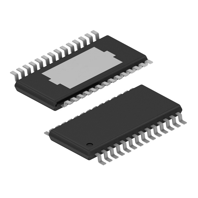
Device Information(1)
PART NUMBER
PACKAGE
TLC6C5816-Q1
HTSSOP (28)
Automotive
Automotive
Automotive
Automotive
Automotive
Instrument Clusters
HVAC Control Panels
Interior Faceplate
E-Shifter Indicators
Center Stacks
9.70 mm × 4.40 mm
(1) For all available packages, see the orderable addendum at
the end of the data sheet.
Typical Application Schematic
Battery 5 V–40 V
3 V–5.5 V
2 Applications
•
•
•
•
•
BODY SIZE (NOM)
VCC
DRAIN0
EN
RCK
DRAIN1/
DIAG0
SER IN
SRCK
MCU
CLR
TLC6C5816-Q1
SER OUT
3 Description
ERR
There are various LED indicators in automotive
applications. Some applications such as hybrid
instrument clusters and E-shifters have safety
requirements which must have LED fault diagnostics;
other applications such as HVAC panels only have an
LED on-off control, which does not require LED
diagnostics. To cover both applications, the
TLC6C5816-Q1 device implements a flexible LED
diagnostics function. By writing to the registers, the
output channels can be configured with LED
diagnostics features or without LED diagnostics
features.
G1
DRAIN14
DRAIN15/
DIAG14
G2
GND
Copyright © 2017, Texas Instruments Incorporated
1
An IMPORTANT NOTICE at the end of this data sheet addresses availability, warranty, changes, use in safety-critical applications,
intellectual property matters and other important disclaimers. PRODUCTION DATA.
�TLC6C5816-Q1
SLASEJ5B – OCTOBER 2017 – REVISED JANUARY 2020
www.ti.com
Table of Contents
1
2
3
4
5
6
7
Features ..................................................................
Applications ...........................................................
Description .............................................................
Revision History.....................................................
Pin Configuration and Functions .........................
Specifications.........................................................
1
1
1
2
3
4
6.1
6.2
6.3
6.4
6.5
6.6
6.7
6.8
4
4
4
5
5
6
6
7
Absolute Maximum Ratings ......................................
ESD Ratings ............................................................
Recommended Operating Conditions.......................
Thermal Information ..................................................
Electrical Characteristics...........................................
Timing Requirements ...............................................
Switching Characteristics ..........................................
Typical Characteristics ..............................................
Detailed Description ............................................ 10
7.1 Overview ................................................................. 10
7.2 Functional Block Diagram ....................................... 10
7.3 Feature Description................................................. 10
7.4 Device Functional Modes........................................ 15
7.5 Register Maps ......................................................... 15
7.6 Interface Registers .................................................. 15
8
Application and Implementation ........................ 20
8.1 Application Information............................................ 20
8.2 Typical Application ................................................. 20
9 Power Supply Recommendations...................... 23
10 Layout................................................................... 24
10.1 Layout Guidelines ................................................. 24
10.2 Layout Example .................................................... 24
11 Device and Documentation Support ................. 25
11.1
11.2
11.3
11.4
11.5
Receiving Notification of Documentation Updates
Community Resources..........................................
Trademarks ...........................................................
Electrostatic Discharge Caution ............................
Glossary ................................................................
25
25
25
25
25
12 Mechanical, Packaging, and Orderable
Information ........................................................... 26
4 Revision History
NOTE: Page numbers for previous revisions may differ from page numbers in the current version.
Changes from Revision A (December 2017) to Revision B
•
Added the functional safety link to the Features section ....................................................................................................... 1
Changes from Original (October 2017) to Revision A
•
2
Page
Page
Changed data sheet from Advance Information to Production Data...................................................................................... 1
Submit Documentation Feedback
Copyright © 2017–2020, Texas Instruments Incorporated
Product Folder Links: TLC6C5816-Q1
�TLC6C5816-Q1
www.ti.com
SLASEJ5B – OCTOBER 2017 – REVISED JANUARY 2020
5 Pin Configuration and Functions
PWP PowerPAD™ Package
28-Pin HTSSOP With Exposed Thermal Pad
Top View
VCC
1
28
GND
G1
2
27
ERR
G2
3
26
NC
DRAIN0
4
25
DRAIN15/DIAG14
DRAIN1/DIAG0
5
24
DRAIN14
DRAIN2
6
23
DRAIN13/DIAG12
DRAIN3/DIAG2
7
22
DRAIN12
21
DRAIN11/DIAG10
Thermal
DRAIN4
8
DRAIN5/DIAG4
9
20
DRAIN10
DRAIN6
10
19
DRAIN9/DIAG8
DRAIN7/DIAG6
11
18
DRAIN8
SER_IN
12
17
SRCK
CLR
13
16
RCK
EN
14
15
SER_OUT
Pad
Not to scale
Pin Functions
PIN
NAME
NO.
I/O
DESCRIPTION
I
Shift register clear, active-low. CLR low level clears all the storage registers in the device,
shift registers work normally. CLR high level makes both storage registers and shift registers
work normally.
CLR
13
DRAIN0
4
O
Channel 0 open drain-output
DRAIN1/DIAG0
5
I/O
Channel 1 open-drain output or diagnostics input 0
DRAIN2
6
O
Channel 2 open drain output
DRAIN3/DIAG2
7
I/O
Channel 3 open-drain output or diagnostics input 2
DRAIN4
8
O
Channel 4 open drain output
DRAIN5/DIAG4
9
I/O
Channel 5 open-drain output or diagnostics input 4
DRAIN6
10
O
Channel 6 open-drain output
DRAIN7/DIAG6
11
I/O
Channel 7 open-drain output or diagnostics input 6
DRAIN8
18
O
Channel 8 open-drain output
DRAIN9/DIAG8
19
I/O
Channel 9 open-drain output or diagnostics input 8
DRAIN10
20
O
Channel 10 open-drain output
DRAIN11/DIAG10
21
I/O
Channel 11 open-drain output or diagnostics input 10
DRAIN12
22
O
Channel 12 open-drain output
DRAIN13/DIAG12
23
I/O
Channel 13 open-drain output or diagnostics input 12
DRAIN14
24
O
Channel 14 open-drain output
DRAIN15/DIAG14
25
I/O
Channel 15 open-drain output or diagnostics input 14
Submit Documentation Feedback
Copyright © 2017–2020, Texas Instruments Incorporated
Product Folder Links: TLC6C5816-Q1
3
�TLC6C5816-Q1
SLASEJ5B – OCTOBER 2017 – REVISED JANUARY 2020
www.ti.com
Pin Functions (continued)
PIN
NAME
NO.
I/O
DESCRIPTION
EN
14
I
Device enable, active-low. EN high level shuts down the device, all the registers reset, and
the device enters standby mode. EN low level enables the device, all functions work
normally.
ERR
27
O
Open-drain error feedback
G1
2
I
Channel enable, controls DRAIN0–DRAIN7 outputs, active-low
G2
3
I
Channel enable, controls DRAIN8–DRAIN15 outputs, active-low
NC
26
NC
RCK
16
I
Serial data latch. The data in each shift register transfers to a storage register at the rising
edge of RCK. Meanwhile, the status bit is loaded to the shift register.
SER IN
12
I
Serial data input. Data on SER IN loads into the shift register on each rising edge of SRCK.
SER OUT
15
O
Serial data output. The purpose of this pin is to cascade several devices on the serial bus.
SRCK
17
I
Serial clock input. On each rising SRCK edge, data transfers from SER IN to the internal
serial shift registers.
VCC
1
P
Power supply pin for the device. Add a 0.1-μF ceramic capacitor near the pin.
GND
28
G
Power ground, the ground reference pin for the device. This pin must connect to the ground
plane on the PCB.
Thermal pad
—
—
Connect to polygon pour to optimize thermal performance
No intenal connection
6 Specifications
6.1 Absolute Maximum Ratings
over operating ambient temperature range (unless otherwise noted) (1)
MIN
MAX
VCC
Supply voltage
–0.3
6
V
VI
Logic input voltage, CLR, EN, G1, G2, RCK, SER IN, SRCK
–0.3
6
V
VO
Logic output voltage, SER OUT
–0.3
VCC + 0.3
V
VDS
Power DMOS drain-source voltage, DRAIN0–DRAIN15
–0.3
45
V
VERR
Error output voltage, ERR
–0.3
6
V
IO
Channel output current
50
mA
Operating junction temperature, TJ
–40
150
°C
Storage temperature, Tstg
–55
165
°C
(1)
UNIT
Stresses beyond those listed under Absolute Maximum Ratings may cause permanent damage to the device. These are stress ratings
only, which do not imply functional operation of the device at these or any other conditions beyond those indicated under Recommended
Operating Conditions. Exposure to absolute-maximum-rated conditions for extended periods may affect device reliability.
6.2 ESD Ratings
VALUE
V(ESD)
(1)
Electrostatic discharge
Human-body model (HBM), per AEC Q100-002 (1)
±4000
Charged-device model (CDM), per AEC Q100011
±1000
All pins
UNIT
V
AEC Q100-002 indicates that HBM stressing shall be in accordance with the ANSI/ESDA/JEDEC JS-001 specification.
6.3 Recommended Operating Conditions
over operating ambient temperature range (unless otherwise noted)
VCC
Supply voltage
VIH
High-level input voltage, CLR, EN, G1, G2, RCK, SER IN, SRCK
VIL
Low-level input voltage, CLR, EN, G1, G2, RCK, SER IN, SRCK
TA
Operating ambient temperature
4
MIN
MAX
3
5.5
2.4
–40
Submit Documentation Feedback
UNIT
V
V
0.7
V
125
°C
Copyright © 2017–2020, Texas Instruments Incorporated
Product Folder Links: TLC6C5816-Q1
�TLC6C5816-Q1
www.ti.com
SLASEJ5B – OCTOBER 2017 – REVISED JANUARY 2020
6.4 Thermal Information
TLC6C5816-Q1
THERMAL METRIC (1)
PWP (HTSSOP)
UNIT
28 PINS
RθJA
Junction-to-ambient thermal resistance
44.4
°C/W
RθJC(top)
Junction-to-case (top) thermal resistance
29.9
°C/W
RθJB
Junction-to-board thermal resistance
26.9
°C/W
ψJT
Junction-to-top characterization parameter
2
°C/W
ψJB
Junction-to-board characterization parameter
26.7
°C/W
RθJC(bot)
Junction-to-case (bottom) thermal resistance
5.3
°C/W
(1)
For more information about traditional and new thermal metrics, see Semiconductor and IC Package Thermal Metrics.
6.5 Electrical Characteristics
VCC = 5 V, TJ = –40°C to 150°C unless otherwise specified
PARAMETER
TEST CONDITIONS
MIN
V(POR-rising)
Power-on-reset rising
threshold
1.5
V(POR-falling)
Power-on-reset falling
threshold
1
t(device-ready)
Device ready time
TYP
MAX
2.5
UNIT
V
V
VCC > 0.5 V, EN = 0
50
All outputs off, no clock signal , EN = 0
60
120
µs
All outputs on, no clock signal, EN = 0
210
300
320
600
µA
1
µA
ICC
Logic supply current
ICC(FRQ)
Logic supply current at
frequency
fSRCK = 5 MHz, CL = 30 pF, all outputs on
I(Q)
Quiescent current
EN = 1
VOH
High-level output voltage
SER OUT
IOH = –20 μA
4.9
4.99
IOH = –4 mA
4.5
4.69
VOL
Low-level output voltage
SER OUT
IOH = –20 μA
0.001
0.01
IOH = –4 mA
0.25
0.4
IIH
High-level input current
VI = 5 V
0.2
µA
IIL
Low-level input current
VI = 0 V
–0.2
µA
ID(SX)
Off-state drain current
VDS = 30 V
0.01
0.1
0.1
0.3
6.2
8
rDS(on)
Static drain-source onstate resistance
VDS = 30 V, TA = 125°C
VCC = 5 V, ID = 20 mA
VCC = 3.3 V, ID = 20 mA
µA
V
TA = 25°C, single channel ON
5
TA = 25°C, all channels ON
6
7.3
9
TA = 125°C, all channels ON
9
11.6
13.5
V
µA
Ω
T(SHUTDOWN)
Thermal shutdown
threshold
175
°C
T(HYS)
Thermal shutdown
hysteresis
15
°C
V(OC_th)
LED-open detection
threshold
Vhys(OC)
LED-open detectionthreshold hysteresis
V(SC_th)
LED-short detection
threshold
Vhys(SC)
LED-short detectionthreshold hysteresis
V(ERR_PD)
ERR pin open-drain
voltage drop
IERR = 4 mA
Ilkg(ERR)
ERR pin leakage current
VERR = 5 V
4
4.3
4.5
60
1
1.22
mV
1.5
60
–1
Product Folder Links: TLC6C5816-Q1
V
mV
0.3
V
1
µA
Submit Documentation Feedback
Copyright © 2017–2020, Texas Instruments Incorporated
V
5
�TLC6C5816-Q1
SLASEJ5B – OCTOBER 2017 – REVISED JANUARY 2020
www.ti.com
6.6 Timing Requirements
Vcc = 5 V, TJ = 25°C, CL = 30 pF, ID = 20 mA unless otherwise specified
MIN
fSRCK
Serial clock frequency
tSRCK
Serial clock duration
tSRCKH
NOM
MAX
UNIT
10
MHz
100
ns
SRCK pulse duration, high
30
ns
tSRCKL
SRCK pulse duration, low
30
ns
tsu
Setup time, SER IN high before SRCK rise
15
ns
th
Hold time, SER IN high after SRCK rise
15
ns
tSER IN
SER IN pulse duration
40
ns
td
Last SRCK rise to RCK rise
200
ns
6.7 Switching Characteristics
Vcc = 5 V, TJ = 25ºC, CL = 30 pF, ID = 20 mA unless otherwise specified
PARAMETER
MIN
TYP
MAX
UNIT
tpd(deg_open)
LED open to ERR pin pulled down time
35
µs
tpd(deg_short)
LED short to ERR pin pulled down time
tpd(GOFF)
Propagation delay time, output off (VOUT equals 10% LED supply
voltage) from Gx rising
35
µs
250
ns
tpd(GON)
Propagation delay time, output on (VOUT equals 90% LED supply
voltage) from Gx falling
250
ns
tpd(ROFF)
Propagation delay time, output off (VOUT equals 10% LED supply
voltage) from RCK rising
250
ns
tpd(RON)
Propagation delay time, output on (VOUT equals 90% LED supply
voltage) from RCK rising
250
ns
tr
Rise time, drain output
100
ns
tf
Fall time, drain output
100
ns
tpd(SIO)
Propagation delay time, SRCK falling edge to SEROUT change
35
ns
tr(o)
SEROUT rise time (10% to 90%)
20
ns
tf(o)
SEROUT fall time (90% to 10%)
20
ns
ttSRC Kt
SRCK
ttsut
ttht
ttSRC KHt
ttSRC KLt
SER IN
ttSER INt
ttdt
RCK
Copyright © 201 7, Texas Instrumen ts Incorpor ate d
Figure 1. Timing Diagram of Input Signals
6
Submit Documentation Feedback
Copyright © 2017–2020, Texas Instruments Incorporated
Product Folder Links: TLC6C5816-Q1
�TLC6C5816-Q1
www.ti.com
SLASEJ5B – OCTOBER 2017 – REVISED JANUARY 2020
Gx
tpd(GOFF)
tpd(GON)
VOUTx
tr
tf
RCK
tpd(ROFF)
tpd(RON)
VOUTx
SRCK
tpd(SIO)
ttpd(SIO)t
SER OUT
tf(o)
tr(o)
Copyright © 201 7, Texas Instrumen ts Incorpor ate d
Figure 2. Timing Diagram of Output Signals
6.8 Typical Characteristics
120
350
40°C
25°C
125°C
340
100
320
Supply Current (PA)
Supply Current (PA)
330
310
300
290
280
270
90
80
70
60
50
260
40
250
30
240
0
0.5
1
VCC = 3 V
VCC = 3.3 V
VCC = 5 V
VCC = 5.5 V
110
1.5
2
2.5
3
3.5
Frequency (MHz)
4
4.5
5
20
-40
-20
D001
0
20
40
60
80
100
Ambient Temperature (°C)
120
140
D002
VCC = 5 V
Figure 3. Supply Current vs CLK Frequency
Figure 4. Supply Current vs Ambient Temperature
Submit Documentation Feedback
Copyright © 2017–2020, Texas Instruments Incorporated
Product Folder Links: TLC6C5816-Q1
7
�TLC6C5816-Q1
SLASEJ5B – OCTOBER 2017 – REVISED JANUARY 2020
www.ti.com
Typical Characteristics (continued)
280
11
All Channels OFF
All Channels ON
10
200
40°C
25°C
125°C
9
rDS(on) (:)
Supply Current (PA)
240
160
8
120
7
80
6
40
3
3.5
4
4.5
5
Supply Voltage (V)
5.5
5
10
6
15
20
D003
VCC = 3.3 V
Figure 5. Supply Current vs Supply Voltage
12
9
11
rDS(on) (:)
rDS(on) (:)
6
40°C
25°C
125°C
9
8
15
20
25
30
35
Drain Current (mA)
40
45
5
10
50
15
20
D007
Single channel ON
VCC = 3.3 V
Figure 7. rDS(on)vs Ambient Temperature
11
10
10
40°C
25°C
125°C
40
45
50
D009
All channels ON
9
rDS(on) (:
8
25
30
35
Drain Current (mA)
Figure 8. rDS(on)vs Drain Current
11
9
rDS(on) (:)
D006
Single channel ON
6
VCC = 5 V
7
40°C
25°C
125°C
8
7
6
6
5
5
4
15
20
VCC = 5 V
25
30
35
Drain Current (mA)
40
45
50
3
D010
3.5
4
4.5
5
VCC (V)
5.5
D008
All channels ON
Figure 9. rDS(on) vs Drain Current
8
50
7
5
4
10
45
10
40°C
25°C
125°C
7
4
10
40
Figure 6. rDS(on) vs Ambient Temperature
10
8
25
30
35
Drain Current (mA)
Submit Documentation Feedback
Figure 10. rDS(on) vs Supply Voltage
Copyright © 2017–2020, Texas Instruments Incorporated
Product Folder Links: TLC6C5816-Q1
�TLC6C5816-Q1
www.ti.com
SLASEJ5B – OCTOBER 2017 – REVISED JANUARY 2020
Typical Characteristics (continued)
6
0.26
VCC = 3 V
VCC = 3.3 V
5.5
VCC = 4 V
VCC = 4.5 V
VCC = 5 V
VCC = 5.5 V
0.24
4.5
VOL (V)
VOH (V)
5
4
0.22
VCC = 3 V
VCC = 3.3 V
VCC = 4 V
VCC = 4.5 V
VCC = 5 V
VCC = 5.5 V
0.2
3.5
0.18
3
2.5
-40
-20
0
20
40
60
80
100
Ambient Temperature (°C)
120
140
0.16
-40
-20
D004
Figure 11. SER OUT High Voltage vs Temperature (°C)
0
20
40
60
80
100
Ambient Temperature (°C)
120
140
D005
Figure 12. SER OUT Low Voltage vs Temperature (°C)
Submit Documentation Feedback
Copyright © 2017–2020, Texas Instruments Incorporated
Product Folder Links: TLC6C5816-Q1
9
�TLC6C5816-Q1
SLASEJ5B – OCTOBER 2017 – REVISED JANUARY 2020
www.ti.com
7 Detailed Description
7.1 Overview
The TLC6C5816-Q1 device is a 16-bit shift-register LED driver designed to support automotive LED applications.
A built-in LED-open and LED-short diagnostic mechanism provides enhanced safety protection. The device
contains 16 channels with power DMOS transistor outputs, but 8 of the channels can instead be configured by
the corresponding DIAGn bits in the Configuration register to support LED fault diagnostics. The diagnostics
channels DIAGn must connect to DRAINn to realize LED diagnostics. A command error fault implies that a
channel is configured for LED diagnostics, but a register write command has turned on the channel at the same
time. The device provides a cyclic redundancy check to verify register values in the shift registers. In readback
mode, the device provides 6 bits of the CRC remainder. The MCU can read back the CRC remainder and check
if the remainder is correct. This checks whether the communication loop between MCU and device is good.
7.2 Functional Block Diagram
TLC6C5816-Q1
VCC
Power
EN
G1
Driver
DRAIN0
Driver
DRAIN1
/DIAG0
G2
Diagnostics
CLR
X8
RCK
SER IN
Logic Control
DRAIN14
SRCK
DRAIN15
/DIAG14
SER OUT
Thermal Shutdown
ERR
Open Drain Error
Output
GND
7.3 Feature Description
The features of the TLC6C5816-Q1 device are described in the following sections. Table 1 describes device
behavior under different conditions.
Table 1. TLC6C5816-Q1 Behavior Under Different Conditions
EN = HIGH
EN̅ = LOW
10
CONFIGUR
ATION
REGISTERS
STATUS
REGISTERS
OUTPUTS 0-7
OUTPUTS 8-15
DEVICE
CURRENT
CLR = X
Clear
Clear
Hi-Z
Hi-Z
Low I(Q)
CLR = LOW
Clear
Clear
Hi-Z
Hi-Z
Active current
Set by fault
detection
Controlled by
configuration and
G1 level
Controlled by
configuration and
G2 level
Operation current
CLR = HIGH
Set by
interface
Submit Documentation Feedback
Copyright © 2017–2020, Texas Instruments Incorporated
Product Folder Links: TLC6C5816-Q1
�TLC6C5816-Q1
www.ti.com
SLASEJ5B – OCTOBER 2017 – REVISED JANUARY 2020
7.3.1 Device Enable (EN)
The TLC6C5816-Q1 device provides a low I(Q) mode. A high EN level shuts down the device, all the registers
reset, and the device enters standby mode. A low EN level enables the device, and all functions work normally.
7.3.2 Gated Output (Gx)
The device provides two active-low inputs to control gated outputs. G1 turns channels DRAIN0–DRAIN7 on and
off, and G2 turns channels DRAIN8–DRAIN15 on and off.
7.3.3 Register Clear (CLR)
The device provides a convenient function for clearing registers. A low CLR input level clears all internal registers
and all fault states. A high CLR level makes the device work normally.
7.3.4 Open-Drain Outputs and Flexible Diagnostics Channel
The device provides 16 output channels. All 16 channels have integrated low-side switches to drive external
loads such as LEDs independently. Eight channels have integrated voltage comparators dedicated for LED-open
and -short diagnostics as depicted in the following sections.
7.3.4.1 Configurable Outputs
The 16 channels are divided into eight pairs of outputs like DRAIN0, DRAIN1/DIAG0 as shown in Figure 13. By
default, both outputs of this pair are open-drain outputs. Each of the pair is independent from the other.
DRAIN1
/DIAG0
REF
DRAIN0
SHORT
OPEN
REF
X8
X8
TLC6C5816-Q1
Copyright © 201 7, Texas Instrumen ts Incorpor ate d
Figure 13. Open-Drain Output and Flexible Diagnostics
By setting its bit in the configuration register to HIGH, the DRAIN1/DIAG0 output can be configured as
diagnostics channel DIAG0 for DRAIN0.
By setting the configuration register to LOW, DRAIN1/DIAG0 can be configured as the independent open-drain
output DRAIN1.
If DRAIN1/DIGA0 is configured as a diagnostics channel, when DRAIN0 is on, the DRAIN1/DIAG0 diagnostics
path monitors the voltage. When DRAIN0 is off, DRAIN1/DIAG0 is in the high-impedance state to avoid any
leakage current.
Submit Documentation Feedback
Copyright © 2017–2020, Texas Instruments Incorporated
Product Folder Links: TLC6C5816-Q1
11
�TLC6C5816-Q1
SLASEJ5B – OCTOBER 2017 – REVISED JANUARY 2020
www.ti.com
Vbat
DRAIN1
/DIAG0
MCU
REF
DRAIN0
SHORT
ERR
4
OPEN
REF
SPI
X8
X8
TLC6C5816-Q1
Copyright © 201 7, Texas Instrumen ts Incorpor ate d
Figure 14. Diagnostics Configuration of Output Driver Pair
7.3.4.2 LED-Open Diagnostics
As depicted in Configurable Outputs, the DIAG0 channel monitors the anode voltage of the LED load of DRAIN0.
When the DRAIN0 channel turns on, DIAG0 compares the DRAIN0 voltage with internal threshold for LED-open
detection, V(OC_th). When DRAIN0 is on, and V(DIAG0) is continuously higher than V(OC_th) for tpd(deg_open), the device
asserts an LED-open fault, sets the corresponding bit in the fault table, and pulls ERR low.
An LED-open fault does not turn off the channel automatically in the LED-open state. Once the device detects an
open fault, it latches the fault status in the DIAGn_OPEN fault register. The fault register value only recovers to
normal when the LED fault disappears and the fault status is read back. Cycling Gx on and off does not clear the
fault.
7.3.4.3 LED-Short Diagnostics
As depicted in Configurable Outputs, the DIAG0 channel monitors the LED anode voltage of DRAIN0. When the
DRAIN0 channel is turned on, DIAG0 compares the DRAIN0 voltage with the internal threshold for LED short
detection, V(SC_th). When DRAIN0 is on and V(DIAG0) is continuously lower than V(SC_th) for tpd(deg_short), the device
asserts an LED-short fault, sets the corresponding bit in the fault flag table, and pulls ERR low.
The device does not turn off the channel automatically in LED-short state. Once device detects a short fault, it
latches the fault state in the DIAGn_SHORT fault register. The fault register value only recovers to normal when
LED fault disappears and the fault status is read back. Cycling Gx on and off does not clear the fault.
7.3.5 Thermal Shutdown
The TLC6C5816-Q1 device has an internal thermal sensor that monitors device temperature. Once the thermal
sensor detects device overtemperature, it disables all channel outputs and sets the TSD flag in the Fault
Readback register. The fault register value only recovers to normal when the overtemperature fault disappears
and the fault status is read back.
7.3.6 Command Error
The diagnostics configuration for DRAINn+1 and DIAGn cannot be set to open-drain output mode and diagnostics
mode at the same time. If the device detects both of the registers have been set high for any channel, the device
sets the CMD_ERR flag HIGH and pulls the open-drain error flag ERR pin low. Furthermore, the device ignores
the DIAGn setting and drives the channel in open-drain output mode. To reset the CMD_ERR flag, correct the
register configuration value and read out the fault register value.
12
Submit Documentation Feedback
Copyright © 2017–2020, Texas Instruments Incorporated
Product Folder Links: TLC6C5816-Q1
�TLC6C5816-Q1
www.ti.com
SLASEJ5B – OCTOBER 2017 – REVISED JANUARY 2020
7.3.7 Serial Communication Error
The device provides a cyclic redundancy check to verify register values in the shift registers. In readback mode,
the device provides 6 bits of the CRC remainder. The MCU can read back the CRC remainder and check if the
remainder is correct to determine whether the communication loop between MCU and device is good. ShiftRegister Communication-Fault Detection gives a detailed description of the CRC check.
7.3.8 Error Feedback
If any of the fault flags is high, ERR is pulled down. The MCU can detect the device fault by this pin, read out
fault flags, and take actions accordingly. The first RCK rising edge latches the fault registers into shift registers.
The status information shifts toward SER OUT at the falling edge of SRCK.
7.3.9 Interface
The TLC6C5816-Q1 device contains a 24-bit shift-register serial interface that feeds a 24-bit D-type storage
register. Data transfer through the shift and storage registers is on the rising edge of the shift register clock
(SRCK) and register latch signal (RCK), respectively. The storage register transfers data to the output buffer
when device enable (EN) is low and shift register clear (CLR) is high.
7.3.9.1 Register Write
The TLC6C5816-Q1 device has a 24-bit configuration register. Data transfers through the shift registers on the
rising edge of SRCK and latches into the storage registers on the rising edge of RCK. The first 8 data bits control
the diagnostics channel configuration, and the following 16 data bits control 16 open-drain outputs independently.
RCK
SRCK
1
SER IN
D23
2
D22
3
D21
4
D20
19
5
D19
D5
20
D4
22
21
D3
D2
23
D1
24
D0
SER OUT
OLD
OUTPUTS
OUTPUT
NEW
OUTPUTS
Copyright © 201 7, Texas Instrumen ts Incorpor ate d
Figure 15. Register Write Timing Diagram
The DRAINn+1-DIAGn channel configuration is controlled by the DIAGn registers. These channels can be set to
either open-drain output or diagnostics input mode. The TLC6C5816-Q1 device does not allow the user to set
DRAINn+1 and DIAGn high at the same time, because the divider resistor for LED diagnostics can result in
leakage current on the LED, which lights up the LED. If the DIAGn and DRAINn registers are set to high at the
same time, the channel operates as an open-drain output instead of LED diagnostics, and a command error
latches in the fault registers, which can be read back by the register readback function as explained in Register
Read.
7.3.9.2 Register Read
The fault information loads to shift registers on the rising edge of RCK and can be read out on SER OUT. On the
rising edge of the RCK signal, the MSB data DIAG14_OPEN appears on the SER OUT pin. On each falling edge
of SRCK signal, there is 1 bit of data shifted out on the SER OUT pin. There is a total of 24 bits in the fault
information registers. Register Maps describes the details.
Submit Documentation Feedback
Copyright © 2017–2020, Texas Instruments Incorporated
Product Folder Links: TLC6C5816-Q1
13
�TLC6C5816-Q1
SLASEJ5B – OCTOBER 2017 – REVISED JANUARY 2020
www.ti.com
RCK
SRCK
1
2
3
4
19
5
20
22
21
23
24
SER IN
SER OUT
D23
D22
D21
D20
D19
D5
D4
D3
D2
D1
D0
tFault Read back Timing Dia gramt
Copyright © 201 7, Texas Instrumen ts Incorpor ate d
Figure 16. Register Read Timing Diagram
7.3.9.3 Shift-Register Communication-Fault Detection
The TLC6C5816-Q1 device provides a cyclic redundancy check to verify register values in the shift registers. In
readback mode, the TLC6C5816-Q1 device provides 6 bits of the CRC remainder. The MCU can read back the
CRC remainder and check if the remainder is correct. The CRC checksum provides a readback method to verify
shift register values without altering them.
Polynomial: x 6 + x + 1
D
D
(1)
D
D
D
D
Input
Copyright © 201 7, Texas Instrumen ts Incorpor ate d
Figure 17. CRC Check Block Diagram
The TLC6C5816-Q1 device also checks the configuration register for faulty commands.
The TLC6C5816-Q1 configuration register consists of 24 bits. To generate the CRC checksum, the device first
shifts left 6 bits and appends 0s, then bit-wise exclusive-ORs the 30 data bits with the polynomial to get the
checksum.
For example, if the configuration data is 0xD7i0F68 and the polynomial is 0x43 (7’b100i0011), the CRC
checksum is 0x19 (6’b01i1001).
The MCU can read back the CRC checksum and append it to the LSB of 24 bits, and then the 30 bits of data
becomes 0x35C3 DA19. Performing the bit-wise exclusive-OR operation with the polynomial should lead to a
residual of 0.
CRC reference: CRC Implementation With MSP430
7.3.9.4 Clear Register
A logic low on CLR clears all registers in the device. TI suggests clearing the device registers during power up or
initialization.
7.3.9.5 Register Clock
RCK is the storage-register clock. Data in the storage register appears at the output whenever the output enable
(G1 and G2) input signals are low.
14
Submit Documentation Feedback
Copyright © 2017–2020, Texas Instruments Incorporated
Product Folder Links: TLC6C5816-Q1
�TLC6C5816-Q1
www.ti.com
SLASEJ5B – OCTOBER 2017 – REVISED JANUARY 2020
7.4 Device Functional Modes
7.4.1 Normal Operation
To make the device operate normally, usually use a 3.3-V or 5-V power supply to power VCC, connect the LED
supply voltage to a regulated voltage or directly to the car battery, and make sure the channel current does not
exceed 50 mA.
7.4.2 POR Reset
When VCC is lower than V(POR-falling), the device stops working and enters the power-off mode. When VCC is higher
than V(POR-rising), the device starts to work and sets all registers to their default values.
7.4.3 Standby Mode
When VCC is higher than V(POR-rising) and EN is high, the device enters the standby mode and sets all registers to
their default values. The power consumption is very low.
7.5 Register Maps
Table 2. Register Map
CONFIGURATION REGISTER
Bit
23
22
21
20
19
18
17
16
Field name
DIAG14
DIAG12
DIAG10
DIAG8
DIAG6
DIAG4
DIAG2
DIAG0
Default
value
0h
0h
0h
0h
0h
0h
0h
0h
Bit
15
14
13
12
11
10
9
8
Field name
DRAIN15
DRAIN14
DRAIN13
DRAIN12
DRAIN11
DRAIN10
DRAIN9
DRAIN8
Default
value
0h
0h
0h
0h
0h
0h
0h
0h
Bit
7
6
5
4
3
2
1
0
Field name
DRAIN7
DRAIN6
DRAIN5
DRAIN4
DRAIN3
DRAIN2
DRAIN1
DRAIN0
Default
value
0h
0h
0h
0h
0h
0h
0h
0h
FAULT_READBACK REGISTER
Bit
23
22
21
20
19
18
17
16
Field name
DIAG14_
OPEN
DIAG14_
SHORT
DIAG12_
OPEN
DIAG12_
SHORT
DIAG10_
OPEN
DIAG10_
SHORT
DIAG8_OPEN
DIAG8_
SHORT
Default
value
0h
0h
0h
0h
0h
0h
0h
0h
Bit
15
14
Field name DIAG6_OPEN
Default
value
13
12
11
10
9
8
DIAG6_
SHORT
DIAG4_OPEN
DIAG4_
SHORT
DIAG2_OPEN
DIAG2_
SHORT
DIAG0_OPEN
DIAG0_
SHORT
0h
0h
0h
0h
0h
0h
0h
5
4
3
2
1
0
0h
Bit
7
6
Field name
TSD
CMD_ERR
CRC
Default
value
0h
0h
0h
7.6 Interface Registers
Table 3 lists the memory-mapped registers for the interface.
Submit Documentation Feedback
Copyright © 2017–2020, Texas Instruments Incorporated
Product Folder Links: TLC6C5816-Q1
15
�TLC6C5816-Q1
SLASEJ5B – OCTOBER 2017 – REVISED JANUARY 2020
www.ti.com
Table 3. Interface Registers
OFFSET
ACRONYM
REGISTER NAME
SECTION
0h
Config
Configuration Register
Go
1h
Fault_Readback
Fault Readback Register
Go
Complex bit access types are encoded to fit into small table cells. Table 4 shows the codes that are used for
access types in this section.
Table 4. Interface Access Type Codes
CODE
DESCRIPTION
Read type
R
Read-only
Read to clear
RC
Read to clear the fault
Write type
W
Write-only
Reset or Default -n
Value
Value after reset or the default
value
7.6.1 Configuration Register (Offset = 0h) [reset = 0h]
Config is shown in Figure 18 and described in Table 5.
Return to Summary Table.
Figure 18. Configuration Register
23
DIAG14
W-0h
22
DIAG12
W-0h
21
DIAG10
W-0h
20
DIAG8
W-0h
19
DIAG6
W-0h
18
DIAG4
W-0h
17
DIAG2
W-0h
16
DIAG0
W-0h
15
DRAIN15
W-0h
14
DRAIN14
W-0h
13
DRAIN13
W-0h
12
DRAIN12
W-0h
11
DRAIN11
W-0h
10
DRAIN10
W-0h
9
DRAIN9
W-0h
8
DRAIN8
W-0h
7
DRAIN7
W-0h
6
DRAIN6
W-0h
5
DRAIN5
W-0h
4
DRAIN4
W-0h
3
DRAIN3
W-0h
2
DRAIN2
W-0h
1
DRAIN1
W-0h
0
DRAIN0
W-0h
Table 5. Configuration Register Field Descriptions
Bit
16
Field
Type
Reset
Description
23
DIAG14
W
0h
Diagnostics configuration bit for DRAIN15 and DIAG14
HIGH = Diagnostics enabled as DIAG14
LOW = Diagnostics disabled as DRAIN15
22
DIAG12
W
0h
Diagnostics configuration bit for DRAIN13 and DIAG12
HIGH = Diagnostics enabled as DIAG12
LOW = Diagnostics disabled as DRAIN13
21
DIAG10
W
0h
Diagnostics configuration bit for DRAIN11 and DIAG10
HIGH = Diagnostics enabled as DIAG10
LOW = Diagnostics disabled as DRAIN11
20
DIAG8
W
0h
Diagnostics configuration bit for DRAIN9 and DIAG8
HIGH = Diagnostics enabled as DIAG8
LOW = Diagnostics disabled as DRAIN9
19
DIAG6
W
0h
Diagnostics configuration bit for DRAIN7 and DIAG6
HIGH = Diagnostics enabled as DIAG16
LOW = Diagnostics disabled as DRAIN7
18
DIAG4
W
0h
Diagnostics configuration bit for DRAIN5 and DIAG4
HIGH = Diagnostics enabled as DIAG4
LOW = Diagnostics disabled as DRAIN5
Submit Documentation Feedback
Copyright © 2017–2020, Texas Instruments Incorporated
Product Folder Links: TLC6C5816-Q1
�TLC6C5816-Q1
www.ti.com
SLASEJ5B – OCTOBER 2017 – REVISED JANUARY 2020
Table 5. Configuration Register Field Descriptions (continued)
Bit
Field
Type
Reset
Description
17
DIAG2
W
0h
Diagnostics configuration bit for DRAIN3 and DIAG2
HIGH = Diagnostics enabled as DIAG2
LOW = Diagnostics disabled as DRAIN3
16
DIAG0
W
0h
Diagnostics configuration bit for DRAIN1 and DIAG0
HIGH = Diagnostics enabled as DIAG0
LOW = Diagnostics disabled as DRAIN1
15
DRAIN15
W
0h
Open-drain output control bit for DRAIN15 and DIAG14
HIGH = Output power switch enabled
LOW = Output power switch disabled
14
DRAIN14
W
0h
Open-drain output control bit for DRAIN14
HIGH = Output power switch enabled
LOW = Output power switch disabled
13
DRAIN13
W
0h
Open-drain output control bit for DRAIN13 and DIAG12
HIGH = Output power switch enabled
LOW = Output power switch disabled
12
DRAIN12
W
0h
Open-drain output control bit for DRAIN12
HIGH = Output power switch enabled
LOW = Output power switch disabled
11
DRAIN11
W
0h
Open-drain output control bit for DRAIN11 and DIAG10
HIGH = Output power switch enabled
LOW = Output power switch disabled
10
DRAIN10
W
0h
Open-drain output control bit for DRAIN10
HIGH = Output power switch enabled
LOW = Output power switch disabled
9
DRAIN9
W
0h
Open-drain output control bit for DRAIN9 and DIAG8
HIGH = Output power switch enabled
LOW = Output power switch disabled
8
DRAIN8
W
0h
Open-drain output control bit for DRAIN8
HIGH = Output power switch enabled
LOW = Output power switch disabled
7
DRAIN7
W
0h
Open-drain output control bit for DRAIN7 and DIAG6
HIGH = Output power switch enabled
LOW = Output power switch disabled
6
DRAIN6
W
0h
Open-drain output control bit for DRAIN6
HIGH = Output power switch enabled
LOW = Output power switch disabled
5
DRAIN5
W
0h
Open-drain output control bit for DRAIN5 and DIAG4
HIGH = Output power switch enabled
LOW = Output power switch disabled
4
DRAIN4
W
0h
Open-drain output control bit for DRAIN4
HIGH = Output power switch enabled
LOW = Output power switch disabled
3
DRAIN3
W
0h
Open-drain output control bit for DRAIN3 DIAG2
HIGH = Output power switch enabled
LOW = Output power switch disabled
2
DRAIN2
W
0h
Open-drain output control bit for DRAIN2
HIGH = Output power switch enabled
LOW = Output power switch disabled
1
DRAIN1
W
0h
Open-drain output control bit for DRAIN1 DIAG0
HIGH = Output power switch enabled
LOW = Output power switch disabled
0
DRAIN0
W
0h
Open-drain output control bit for DRAIN0
HIGH = Output power switch enabled
LOW = Output power switch disabled
Submit Documentation Feedback
Copyright © 2017–2020, Texas Instruments Incorporated
Product Folder Links: TLC6C5816-Q1
17
�TLC6C5816-Q1
SLASEJ5B – OCTOBER 2017 – REVISED JANUARY 2020
www.ti.com
7.6.2 Fault Readback Register (Offset = 1h) [reset = 0h]
Fault_readback is shown in Figure 19 and described in Table 6.
Return to Summary Table.
Figure 19. Fault_Readback Register
23
22
21
20
19
18
DIAG14_OPEN DIAG14_SHOR DIAG12_OPEN DIAG12_SHOR DIAG10_OPEN DIAG10_SHOR
T
T
T
RC-0h
RC-0h
RC-0h
RC-0h
RC-0h
RC-0h
17
DIAG8_OPEN
16
DIAG8_SHORT
RC-0h
RC-0h
15
DIAG6_OPEN
RC-0h
14
DIAG6_SHORT
RC-0h
13
DIAG4_OPEN
RC-0h
12
DIAG4_SHORT
RC-0h
11
DIAG2_OPEN
RC-0h
10
DIAG2_SHORT
RC-0h
9
DIAG0_OPEN
RC-0h
8
DIAG0_SHORT
RC-0h
7
TSD
RC-0h
6
CMD_ERR
RC-0h
5
4
3
2
1
0
CRC
R-0h
Table 6. Fault Readback Register Field Descriptions
18
Bit
Field
Type
Reset
Description
23
DIAG14_OPEN
RC
0h
LED-Open fault flag for DRAIN15 and DIAG14, read to clear the fault
HIGH = LED-open fault detected
LOW = LED-open fault not detected
22
DIAG14_SHORT
RC
0h
LED-short fault flag for DIAG15 and DIAG14, read to clear the fault
HIGH = LED-short fault detected
LOW = LED-short fault not detected
21
DIAG12_OPEN
RC
0h
LED-open fault flag for DRAIN13 and DIAG12, read to clear the fault
HIGH = LED open fault detected
LOW = LED-open fault not detected
20
DIAG12_SHORT
RC
0h
LED-short fault flag for DIAG13 and DIAG12, read to clear the fault
HIGH = LED-short fault detected
LOW = LED-short fault not detected
19
DIAG10_OPEN
RC
0h
LED-open fault flag for DRAIN11 and DIAG10, read to clear the fault
HIGH = LED-open fault detected
LOW = LED-open fault not detected
18
DIAG10_SHORT
RC
0h
LED-short fault flag for DIAG11 and DIAG10, read to clear the fault
HIGH = LED-short fault detected
LOW = LED-short fault not detected
17
DIAG8_OPEN
RC
0h
LED-open fault flag for DRAIN9 and DIAG8, read to clear the fault
HIGH = LED-open fault detected
LOW = LED-open fault not detected
16
DIAG8_SHORT
RC
0h
LED-short fault flag for DIAG9 and DIAG8, read to clear the fault
HIGH = LED-short fault detected
LOW = LED-short fault not detected
15
DIAG6_OPEN
RC
0h
LED-open fault flag for DRAIN7 and DIAG6, read to clear the fault
HIGH = LED-open fault detected
LOW = LED-open fault not detected
14
DIAG6_SHORT
RC
0h
LED-short fault flag for DIAG7 and DIAG6, read to clear the fault
HIGH = LED-short fault detected
LOW = LED-short fault not detected
13
DIAG4_OPEN
RC
0h
LED-open fault flag for DRAIN5 and DIAG4, read to clear the fault
HIGH = LED open fault detected
LOW = LED-open fault not detected
12
DIAG4_SHORT
RC
0h
LED-short fault flag for DIAG5 and DIAG4, read to clear the fault
HIGH = LED-short fault detected
LOW = LED-short fault not detected
Submit Documentation Feedback
Copyright © 2017–2020, Texas Instruments Incorporated
Product Folder Links: TLC6C5816-Q1
�TLC6C5816-Q1
www.ti.com
SLASEJ5B – OCTOBER 2017 – REVISED JANUARY 2020
Table 6. Fault Readback Register Field Descriptions (continued)
Bit
Field
Type
Reset
Description
11
DIAG2_OPEN
RC
0h
LED-open fault flag for DRAIN3 and DIAG2, read to clear the fault
HIGH = LED-open fault detected
LOW = LED-open fault not detected
10
DIAG2_SHORT
RC
0h
LED-short fault flag for DIAG3 and DIAG2, read to clear the fault
HIGH = LED-short fault detected
LOW = LED-short fault not detected
9
DIAG0_OPEN
RC
0h
LED-open fault flag for DRAIN1 and DIAG0, read to clear the fault
HIGH = LED-open fault detected
LOW = LED-open fault not detected
8
DIAG0_SHORT
RC
0h
LED-short fault flag for DIAG1 and DIAG0, read to clear the fault
HIGH = LED-short fault detected
LOW = LED-short fault not detected
7
TSD
RC
0h
Thermal-shutdown detection flag, read to clear the fault
HIGH = Thermal shutdown detected
LOW = Thermal shutdown not detected
6
CMD_ERR
RC
0h
Serial-interface command error, read to clear the fault
HIGH = Command error detected in last serial-interface
communication
LOW = No command error detected in last serial-interface
communication
CRC
R
0h
CRC checksum of configuration registers
5–0
Submit Documentation Feedback
Copyright © 2017–2020, Texas Instruments Incorporated
Product Folder Links: TLC6C5816-Q1
19
�TLC6C5816-Q1
SLASEJ5B – OCTOBER 2017 – REVISED JANUARY 2020
www.ti.com
8 Application and Implementation
NOTE
Information in the following applications sections is not part of the TI component
specification, and TI does not warrant its accuracy or completeness. TI’s customers are
responsible for determining suitability of components for their purposes. Customers should
validate and test their design implementation to confirm system functionality.
8.1 Application Information
The TLC6C5816-Q1 device usually is used to drive LED indicators in automotive cluster applications to convey
different kinds of information, such as airbag alert, engine fault, and so forth. Typically there are two types LED
indicators, general-purpose indicators and safety-related indicators. General indicators only require a simple
turnon and turnoff function. Safety-related indicators require not only LED on-off control, but also LED-open and short diagnostics. The TLC6C5816-Q1 device is very flexible, as it has 8 configurable LED diagnostics pins,
which can be configured as open-drain outputs or LED open- and short-diagnostics pins. By configuring
corresponding channels for the LED diagnostics function, the TLC6C5816-Q1 device can provide LED open and
short diagnostics to improve the system safety level. The following section describes a typical cluster application.
8.2 Typical Application
Following is a typical automotive cluster application which contains 24 LEDs. Two TLC6C5816-Q1 devices
connected in series drive the total of 24 LEDs. The first device drives 8 safety-critical LEDs which require LED
diagnostics, and the second device drives 16 general-purpose LEDs which only require simple on-and-off control.
An MCU, which controls the two devices through a serial interface and GPIOs, controls channel on-off, PWM
dimming, and LED diagnostics functions.
20
Submit Documentation Feedback
Copyright © 2017–2020, Texas Instruments Incorporated
Product Folder Links: TLC6C5816-Q1
�TLC6C5816-Q1
www.ti.com
SLASEJ5B – OCTOBER 2017 – REVISED JANUARY 2020
Typical Application (continued)
VCC
BATTERY
4.7 …F
GND
GND
0.1 …F
10 …F
GND
GND
VCC
DRA IN0
EN
DIA G0
G1
DRA IN2
G2
DIA G2
CLR
DRA IN4
ERR
DIA G4
DRA IN6
SER IN
SRCK
MCU
GND
TLC6C5816-Q1
DIA G6
RCK
DRA IN8
SER OUT
DIA G8
GND
DRA IN10
GND
DIA G10
DRA IN12
DIA G12
DRA IN14
DIA G14
VCC
0.1 …F
4.7 …F
GND
GND
VCC
DRA IN0
EN
DRA IN1
G1
DRA IN2
G2
DRA IN3
CLR
DRA IN4
ERR
DRA IN5
DRA IN6
SER IN
SRCK
TLC6C5816-Q1
DRA IN7
RCK
DRA IN8
SER OUT
DRA IN9
GND
DRA IN10
GND
DRA IN11
DRA IN12
DRA IN13
DRA IN14
DRA IN15
Copyright © 201 7, Texas Instrumen ts Incorpor ate d
Figure 20. Typical Application Circuit
8.2.1 Design Requirements
Here are the design requirements for the system. The device is powered by 3.3-V voltage. The LED supply is an
automotive battery, 12 V typical. Target LED current is 10 mA typical.
Table 7. Design Requirements
Parameter
Value
VCC
3.3 V
VBATTERY
12 V typical
ILED
10 mA typical
8.2.2 Detailed Design Procedure
Based on the LED supply voltage, LED forward voltage, and LED output current, calculate the value for the
current-setting resistor.
Assume the LED forward voltage is 2 volts, current-setting resistor R = (VBATTERY – VLED) / ILED = 1 kΩ.
8.2.3 Application Curves
This section shows the device normal control waveform and error-state waveform.
Submit Documentation Feedback
Copyright © 2017–2020, Texas Instruments Incorporated
Product Folder Links: TLC6C5816-Q1
21
�TLC6C5816-Q1
SLASEJ5B – OCTOBER 2017 – REVISED JANUARY 2020
www.ti.com
Figure 21. Waveform for Turning On Cascading Device
DRAIN15
22
Figure 22. First Device Drain0 Open Waveform
Submit Documentation Feedback
Copyright © 2017–2020, Texas Instruments Incorporated
Product Folder Links: TLC6C5816-Q1
�TLC6C5816-Q1
www.ti.com
SLASEJ5B – OCTOBER 2017 – REVISED JANUARY 2020
9 Power Supply Recommendations
The supply voltage range is from 3 V to 5.5 V for the TLC6C5816-Q1 device, which typically uses the same
supply voltage as the microcontroller, 3.3 V or 5 V. The LED supply voltage can be up to 40 V, so the LED
supply can use a car battery directly. Ensure the LED current is no greater than 50 mA during load dump
conditions. As the car battery varies a lot, to achieve stable LED brightness, a regulated voltage, for example
5 V, is preferred for the LED supply.
Submit Documentation Feedback
Copyright © 2017–2020, Texas Instruments Incorporated
Product Folder Links: TLC6C5816-Q1
23
�TLC6C5816-Q1
SLASEJ5B – OCTOBER 2017 – REVISED JANUARY 2020
www.ti.com
10 Layout
10.1 Layout Guidelines
To enhance the thermal performance, the TLC6C5816-Q1 device is designed with a thermal pad. TI
recommends to reserve enough copper area for a heat sink. To minimize the noise interference, it is
recommended to put the filter capacitor near the VCC pin. For a detailed layout example, see the following
example.
10.2 Layout Example
VLED up to 40V
VCC = 3 to 5.5V
to µ C
VCC
GND
28
to µ C
2
G1
ERR
27
to µ C
3
G2
4
DRA IN0
5
DRA IN1
DIA G0
6
DRA IN2
7
DRA IN3
DIA G2
8
DRA IN4
9
DRA IN5
DIA G4
10 DRA IN6
DRA IN7
11
DIA G6
TLC6C5816-Q1
1
NC
26
DRA IN15
DIA G14
25
DRA IN14
24
DRA IN13
DIA G12
23
DRA IN12
22
DRA IN11
DIA G10
21
DRA IN10
20
DRA IN9
DIA G8
19
DRA IN8
18
to µ C
12
SER IN
SRCK
17
to µ C
to µ C
13
CLR
RCK
16
to µ C
to µ C
14
EN
SER OUT 15
to µ C
Figure 23. Layout Example
24
Submit Documentation Feedback
Copyright © 2017–2020, Texas Instruments Incorporated
Product Folder Links: TLC6C5816-Q1
�TLC6C5816-Q1
www.ti.com
SLASEJ5B – OCTOBER 2017 – REVISED JANUARY 2020
11 Device and Documentation Support
11.1 Receiving Notification of Documentation Updates
To receive notification of documentation updates, navigate to the device product folder on ti.com. In the upper
right corner, click on Alert me to register and receive a weekly digest of any product information that has
changed. For change details, review the revision history included in any revised document.
11.2 Community Resources
TI E2E™ support forums are an engineer's go-to source for fast, verified answers and design help — straight
from the experts. Search existing answers or ask your own question to get the quick design help you need.
Linked content is provided "AS IS" by the respective contributors. They do not constitute TI specifications and do
not necessarily reflect TI's views; see TI's Terms of Use.
11.3 Trademarks
PowerPAD, E2E are trademarks of Texas Instruments.
All other trademarks are the property of their respective owners.
11.4 Electrostatic Discharge Caution
This integrated circuit can be damaged by ESD. Texas Instruments recommends that all integrated circuits be handled with
appropriate precautions. Failure to observe proper handling and installation procedures can cause damage.
ESD damage can range from subtle performance degradation to complete device failure. Precision integrated circuits may be more
susceptible to damage because very small parametric changes could cause the device not to meet its published specifications.
11.5 Glossary
SLYZ022 — TI Glossary.
This glossary lists and explains terms, acronyms, and definitions.
Submit Documentation Feedback
Copyright © 2017–2020, Texas Instruments Incorporated
Product Folder Links: TLC6C5816-Q1
25
�TLC6C5816-Q1
SLASEJ5B – OCTOBER 2017 – REVISED JANUARY 2020
www.ti.com
12 Mechanical, Packaging, and Orderable Information
The following pages include mechanical, packaging, and orderable information. This information is the mostcurrent data available for the designated device. This data is subject to change without notice and without
revision of this document. For browser-based versions of this data sheet, see the left-hand navigation pane.
26
Submit Documentation Feedback
Copyright © 2017–2020, Texas Instruments Incorporated
Product Folder Links: TLC6C5816-Q1
�PACKAGE OPTION ADDENDUM
www.ti.com
10-Dec-2020
PACKAGING INFORMATION
Orderable Device
Status
(1)
Package Type Package Pins Package
Drawing
Qty
Eco Plan
(2)
Lead finish/
Ball material
MSL Peak Temp
Op Temp (°C)
Device Marking
(3)
(4/5)
(6)
TLC6C5816QPWPRQ1
ACTIVE
HTSSOP
PWP
28
2000
RoHS & Green
NIPDAU
Level-3-260C-168 HR
-40 to 125
TLC6C5816
(1)
The marketing status values are defined as follows:
ACTIVE: Product device recommended for new designs.
LIFEBUY: TI has announced that the device will be discontinued, and a lifetime-buy period is in effect.
NRND: Not recommended for new designs. Device is in production to support existing customers, but TI does not recommend using this part in a new design.
PREVIEW: Device has been announced but is not in production. Samples may or may not be available.
OBSOLETE: TI has discontinued the production of the device.
(2)
RoHS: TI defines "RoHS" to mean semiconductor products that are compliant with the current EU RoHS requirements for all 10 RoHS substances, including the requirement that RoHS substance
do not exceed 0.1% by weight in homogeneous materials. Where designed to be soldered at high temperatures, "RoHS" products are suitable for use in specified lead-free processes. TI may
reference these types of products as "Pb-Free".
RoHS Exempt: TI defines "RoHS Exempt" to mean products that contain lead but are compliant with EU RoHS pursuant to a specific EU RoHS exemption.
Green: TI defines "Green" to mean the content of Chlorine (Cl) and Bromine (Br) based flame retardants meet JS709B low halogen requirements of


 工商网监
湘ICP备2023018690号
工商网监
湘ICP备2023018690号
