Sample &
Buy
Product
Folder
Support &
Community
Tools &
Software
Technical
Documents
TLC5971
SBVS146D – AUGUST 2010 – REVISED DECEMBER 2015
TLC5971 12-Channel, 16-Bit, Enhanced Spectrum, PWM, RGB, LED Driver With 3.3-V
Linear Regulator
1 Features
•
•
•
1
•
•
•
•
•
•
•
•
•
•
•
•
2 Applications
12 Constant-Current Sink Output Channels
Current Capability: 60 mA Per Channel
Grayscale (GS) Control With Enhanced Spectrum
PWM:
16-Bit (65536 Steps)
Global Brightness Control (BC):
7-Bit (128 Steps) for Each Color Group
Power-Supply Voltage Range:
– Internal Linear Regulator: 6 V to 17 V
– Direct Power Supply: 3 V to 5.5 V
LED Supply Voltage: Up to 17 V
Constant-Current Accuracy:
– Channel-to-Channel = ±1% (Typical)
– Device-to-Device = ±1% (Typical)
Data Transfer Rate: 20 MHz
Linear Voltage Regulator: 3.3 V
Auto Display Repeat Function
Display Timing Reset Function
Internal and External Selectable GS Clock
Thermal Shutdown (TSD) With Auto Restart
Unlimited Device Cascading
Operating Temperature Range: –40°C to +85°C
RGB LED Cluster Lamp Displays
3 Description
The TLC5971 device is a 12-channel, constantcurrent sink driver. Each output channel has
individually adjustable currents with 65536 PWM
grayscale (GS) steps. Also, each color group can be
controlled by 128 constant-current sink steps with the
global brightness control (BC) function. GS control
and BC are accessible through a two-wire signal
interface. The maximum current value for each
channel is set by a single external resistor. All
constant-current outputs are turned off when the IC is
in an overtemperature condition.
Device Information(1)
PART NUMBER
TLC5971
PACKAGE
BODY SIZE (NOM)
HTSSOP (20)
6.50 mm × 4.40 mm
VQFN (24)
4.00 mm × 4.00 mm
(1) For all available packages, see the orderable addendum at
the end of the data sheet.
Typical Application Circuit Example (Internal Linear Regulator Using VCC = 6 V to 17 V)
VCC
Power
Supply
(6 V to 17 V)
GND
GND
Device
Optional
VCC
1 mF
GND
VREG
OUTR0
IREF
OUTG0
IREF
OUTG0
¼
¼
OUTR0
¼
VREG
OUTG3
OUTG3
OUTB3
Controller
Optional
VCC
¼
Device
1 mF
OUTB3
DATA
SDTI
SDTO
SDTI
SDTO
CLK
SCKI
SCKO
SCKI
SCKO
(1)
GND
(1)
The output voltage range is from 0 V to 3.3 V.
NOTE: The number of LEDs in series changes, depending on the VCC voltage.
1
An IMPORTANT NOTICE at the end of this data sheet addresses availability, warranty, changes, use in safety-critical applications,
intellectual property matters and other important disclaimers. PRODUCTION DATA.
�TLC5971
SBVS146D – AUGUST 2010 – REVISED DECEMBER 2015
www.ti.com
Table of Contents
1
2
3
4
5
6
Features ..................................................................
Applications ...........................................................
Description .............................................................
Revision History.....................................................
Pin Configuration and Functions .........................
Specifications.........................................................
6.1
6.2
6.3
6.4
6.5
6.6
6.7
6.8
7
1
1
1
2
3
4
Absolute Maximum Ratings ...................................... 4
ESD Ratings.............................................................. 4
Recommended Operating Conditions....................... 4
Thermal Information .................................................. 5
Electrical Characteristics........................................... 5
Switching Characteristics .......................................... 7
Dissipation Ratings ................................................... 8
Typical Characteristics ............................................ 11
Parametric Measurement Information ............... 13
7.1 Test Circuits ............................................................ 13
7.2 Pin Equivalent Input and Output Schematics ......... 13
8
Detailed Description ............................................ 14
8.1 Overview ................................................................. 14
8.2
8.3
8.4
8.5
9
Functional Block Diagram .......................................
Feature Description.................................................
Device Functional Modes........................................
Programming...........................................................
14
15
18
19
Application and Implementation ........................ 26
9.1 Application Information............................................ 26
9.2 Typical Application .................................................. 26
9.3 System Examples ................................................... 31
10 Power Supply Recommendations ..................... 32
11 Layout................................................................... 32
11.1 Layout Guidelines ................................................. 32
11.2 Layout Example .................................................... 32
12 Device and Documentation Support ................. 33
12.1
12.2
12.3
12.4
Community Resources..........................................
Trademarks ...........................................................
Electrostatic Discharge Caution ............................
Glossary ................................................................
33
33
33
33
13 Mechanical, Packaging, and Orderable
Information ........................................................... 33
4 Revision History
NOTE: Page numbers for previous revisions may differ from page numbers in the current version.
Changes from Revision C (September 2012) to Revision D
•
Page
Added Pin Configuration and Functions section, ESD Ratings table, Feature Description section, Device Functional
Modes, Application and Implementation section, Power Supply Recommendations section, Layout section, Device
and Documentation Support section, and Mechanical, Packaging, and Orderable Information section .............................. 1
Changes from Revision B (June 2012) to Revision C
Page
•
Changed typical application circuit (internal linear regulator), added footnote 1.................................................................... 1
•
Changed typical application circuit (direct power), added footnote 1................................................................................... 31
•
Added typical application circuit example (direct power supplying VCC = 3 V to 5.5 V, VLED = 15 V), added footnote 1..... 31
Changes from Revision A (December 2010) to Revision B
Page
•
Changed IOLKG parameter test conditions in Electrical Characteristics table.......................................................................... 5
•
Updated Figure 23................................................................................................................................................................ 15
•
Changed bit 217 description in Table 5................................................................................................................................ 24
Changes from Original (August 2010) to Revision A
Page
•
Changed Global Brightness Control bullet in Features .......................................................................................................... 1
•
Changed typical application circuit (internal linear regulator)................................................................................................. 1
•
Moved Thermal Shutdown and Noise Reduction sections................................................................................................... 18
•
Updated bit names for BCR, BCG, and BCB in Table 5 ...................................................................................................... 24
•
Changed typical application circuit (direct power) ................................................................................................................ 31
2
Submit Documentation Feedback
Copyright © 2010–2015, Texas Instruments Incorporated
Product Folder Links: TLC5971
�TLC5971
www.ti.com
SBVS146D – AUGUST 2010 – REVISED DECEMBER 2015
5 Pin Configuration and Functions
PWP Package
20-Pin HTSSOP
Bottom View
OUTB0
5
GND
17
NC
(1)
3
16
IREF
15
VREG
NC
Thermal Pad
(Bottom Side)
5
14
NC
13
13
VCC
OUTR2
SDTO
6
8
SDTI
9
12
SDTO
SCKI
10
11
SCKO
12
SCKO
OUTB3
OUTG2
11
14
OUTG3
7
9
4
10
NC
OUTB2
OUTB2
OUTR3
15
8
OUTB1
18
2
7
OUTG1
1
OUTR2
6
OUTR3
SDTI
SCKI
OUTG2
OUTR1
16
PowerPAD
(Bottom Side)
OUTR0
OUTG3
19
17
OUTB0
4
OUTG0
OUTB3
OUTG0
20
18
OUTR1
3
21
VCC
OUTR0
22
VREG
19
OUTB1
20
2
OUTG1
1
GND
23
IREF
24
RGE Package
24-Pin VQFN
Bottom View
NC = not connected
Pin Functions
PIN
NAME
I/O
DESCRIPTION
PWP
RGE
SDTI
9
1
I
Serial data input for the 224-bit shift register
SCKI
10
2
I
Serial data shift clock input.
Data present on SDTI are shifted to the LSB of the 224-bit shift register with the SCKI rising edge
Data in the shift register are shifted toward the MSB at each SCKI rising edge.
The MSB data of the shift register appear on SDTO.
SDTO
12
6
O
Serial data output of the 224-bit shift register.
SDTO is connected to the MSB of the 224-bit shift register.
Data are clocked out at the SCKI rising edge.
SCKO
11
5
O
Serial data shift clock output.
The input shift clock signal from SCKI is adjusted to the timing of the serial data output for SDTO
and the signal is then output at SCKO.
I/O
Internal linear voltage regulator output.
A decoupling capacitor of 1 µF must be connected. This output can be used for external devices
as a 3.3-V power supply. This terminal can be connected with the VREG terminal of other
devices to increase the supply current. Also, this pin can be supplied with 3 V to 5.5 V from an
external power supply by connecting it to VCC.
Maximum current programming terminal.
A resistor connected between IREF and GND sets the maximum current for every constantcurrent output. When this terminal is directly connected to GND, all outputs are forced off. The
external resistor should be placed close to the device.
VREG
20
15
IREF
1
16
I/O
OUTR0
3
19
O
OUTR1
6
22
O
OUTR2
13
7
O
OUTR3
16
10
O
OUTG0
4
20
O
OUTG1
7
23
O
OUTG2
14
8
O
OUTG3
17
11
O
OUTB0
5
21
O
OUTB1
8
24
O
OUTB2
15
9
O
OUTB3
18
12
O
VCC
19
13
—
RED constant-current outputs.
Multiple outputs can be configured in parallel to increase the constant-current capability.
Different voltages can be applied to each output.
GREEN constant-current outputs.
Multiple outputs can be configured in parallel to increase the constant-current capability.
Different voltages can be applied to each output.
BLUE constant-current outputs.
Multiple outputs can be configured in parallel to increase the constant-current capability.
Different voltages can be applied to each output.
Power-supply terminal
Submit Documentation Feedback
Copyright © 2010–2015, Texas Instruments Incorporated
Product Folder Links: TLC5971
3
�TLC5971
SBVS146D – AUGUST 2010 – REVISED DECEMBER 2015
www.ti.com
Pin Functions (continued)
PIN
NAME
GND,
PowerPAD
(PWP)
PWP
RGE
2
—
I/O
DESCRIPTION
—
Power ground terminal
GND,
exposed
thermal
pad (RGE)
—
18
—
NC
—
3, 4, 14,
17
—
No internal connection
6 Specifications
6.1 Absolute Maximum Ratings
over operating free-air temperature range, unless otherwise noted. (1) (2)
MIN
MAX
UNIT
–0.3
18
V
IREF
–0.3
VREG + 0.3
V
SDTI, SCKI
–0.3
VREG + 0.6
V
OUTR0 to OUTR3, OUTG0 to OUTG3, OUTB0 to OUTB3
–0.3
18
V
SDTO, SCKO
–0.3
VREG + 0.3
V
VREG
–0.3
6
V
OUTR0 to OUTR3, OUTG0 to OUTG3, OUTB0 to OUTB3
75
mA
VREG
–30
mA
150
°C
150
°C
Supply voltage, VCC
Input voltage
Output voltage
Output current (DC)
Operating junction temperature, TJ (max)
Storage temperature, Tstg
(1)
(2)
–55
Stresses beyond those listed under Absolute Maximum Ratings may cause permanent damage to the device. These are stress ratings
only, and functional operation of the device at these or any other conditions beyond those indicated under Recommended Operating
Conditions is not implied. Exposure to absolute-maximum-rated conditions for extended periods may affect device reliability.
All voltage values are with respect to network ground terminal.
6.2 ESD Ratings
VALUE
V(ESD)
(1)
(2)
Electrostatic
discharge
Human body model (HBM), per ANSI/ESDA/JEDEC JS-001 (1)
±4000
Charged-device model (CDM), per JEDEC specification JESD22-C101 (2)
±2000
UNIT
V
JEDEC document JEP155 states that 500-V HBM allows safe manufacturing with a standard ESD control process.
JEDEC document JEP157 states that 250-V CDM allows safe manufacturing with a standard ESD control process.
6.3 Recommended Operating Conditions
at TA = –40°C to +85°C, and VCC = 6 V to 17 V or VCC = VREG = 3 V to 5.5 V, unless otherwise noted.
MIN
NOM
MAX
UNIT
17
V
3.3
5.5
V
17
V
DC CHARACTERISTICS
VCC
Supply voltage, internal voltage regulator used
6
VREG
Supply voltage, VREG connected to VCC
3
VO
Voltage applied to output
(OUTR0 to OUTR3, OUTG0 to OUTG3, OUTB0 to OUTB3)
VIH
High-level input voltage (SDTI, SCKI)
0.7 × VREG
VREG
V
VIL
Low-level input voltage (SDTI, SCKI)
GND
0.3 × VREG
V
VIHYS
Input voltage hysteresis (SDTI, SCKI)
IOH
High-level output current (SDTO)
–2
mA
IOL
Low-level output current (SDTO)
2
mA
IOLC
Constant output sink current
(OUTR0 to OUTR3, OUTG0 to OUTG3, OUTB0 to OUTB3)
60
mA
4
0.2 × VREG
Submit Documentation Feedback
V
Copyright © 2010–2015, Texas Instruments Incorporated
Product Folder Links: TLC5971
�TLC5971
www.ti.com
SBVS146D – AUGUST 2010 – REVISED DECEMBER 2015
Recommended Operating Conditions (continued)
at TA = –40°C to +85°C, and VCC = 6 V to 17 V or VCC = VREG = 3 V to 5.5 V, unless otherwise noted.
MIN
IREG
Voltage regulator output current (VREG)
TA
Operating free temperature range
TJ
Operating junction temperature
NOM
MAX
UNIT
–25
mA
–40
85
°C
–40
125
°C
0.007
20
MHz
AC CHARACTERISTICS
fCLK
(SCKI)
Data clock frequency and GS control clock frequency, SCKI
tWH/tWL
Pulse duration, SCKI
10
tSU
ns
Setup time, SDTI – SCKI↑
5
tH
ns
Hold time, SDTI – SCKI↑
3
ns
6.4 Thermal Information
TLC5971
THERMAL METRIC
(1)
PWP (HTSSOP)
RGE (VQFN)
20 PINS
24 PINS
UNIT
θJA
Junction-to-ambient thermal resistance
68.6
38
°C/W
θJCtop
Junction-to-case (top) thermal resistance
44.2
40.5
°C/W
θJB
Junction-to-board thermal resistance
19.3
10.2
°C/W
ψJT
Junction-to-top characterization parameter
2.7
0.3
°C/W
ψJB
Junction-to-board characterization parameter
15.7
10
°C/W
θJCbot
Junction-to-case (bottom) thermal resistance
1.8
2.9
°C/W
(1)
For more information about traditional and new thermal metrics, see the Semiconductor and IC Package Thermal Metrics application
report, SPRA953.
6.5 Electrical Characteristics
At TA = –40°C to +85°C, VCC = 6 V to 17 V or VCC = VREG = 3 V to 5.5 V, VLED = 5 V, and CVREG = 1 µF, unless otherwise
noted. Typical values are at TA = 25°C and VCC = 12 V.
PARAMETER
TEST CONDITIONS
VOH
High-level output voltage, SDTO/SCKO
IOH = –2 mA
VOL
Low-level output voltage, SDTO/SCKO
IOL = 2 mA
II
Input current, SDTI/SCKI
VI = VREG or GND
MAX
UNIT
VREG – 0.4
MIN
TYP
VREG
V
0
0.4
V
–1
1
µA
ICC
SDTI/SCKI = low, BLANK = 1, GSn = FFFFh,
BCX = 7Fh, VOUTXn = 1 V, RIREF = 24 kΩ (IOLCMax = 2 mA)
2
4
mA
ICC1
SDTI/SCKI = low, BLANK = 1, GSn = FFFFh,
BCX = 7Fh, VOUTXn = 1 V, RIREF = 1.6 kΩ (IOLCMax = 30 mA)
6
9
mA
ICC2
SDTI = 10 MHz, SCKI = 20 MHz, BLANK = 0,
auto repeat enable, external GS clock selected, GSn = FFFFh,
BCX = 7Fh, VOUTXn = 1 V, RIREF = 1.6 kΩ (IOLCMax = 30 mA)
14
22
mA
ICC3
SDTI = 10 MHz, SCKI = 20 MHz, BLANK = 0,
auto repeat enable, external GS clock selected, GSn = FFFFh,
BCX = 7Fh, VOUTXn = 1 V, RIREF = 0.82 kΩ (IOLCMax = 60 mA)
21
36
mA
60.5
64.7
mA
0.1
µA
Supply current
IOLC
Constant output current, OUTXn
All OUTXn on, BCX = 7Fh, VOUTXn = 1 V,
VOUTfix = 1 V, RIREF = 0.82 kΩ (IOLCMax = 60 mA)
IOLKG
Leakage output current, OUTXn
All OUTXn off, BCX = 7Fh, VOUTXn = 17 V,
VOUTfix = 17 V, RIREF = 0.82 kΩ (IOLCMax = 60 mA)
56.3
Submit Documentation Feedback
Copyright © 2010–2015, Texas Instruments Incorporated
Product Folder Links: TLC5971
5
�TLC5971
SBVS146D – AUGUST 2010 – REVISED DECEMBER 2015
www.ti.com
Electrical Characteristics (continued)
At TA = –40°C to +85°C, VCC = 6 V to 17 V or VCC = VREG = 3 V to 5.5 V, VLED = 5 V, and CVREG = 1 µF, unless otherwise
noted. Typical values are at TA = 25°C and VCC = 12 V.
MIN
TYP
MAX
ΔIOLC
Constant-current error (1)
(channel-to-channel in same color group),
OUTXn
PARAMETER
All OUTXn on, BCX = 7Fh, VOUTXn = VOUTfix = 1 V,
RIREF = 0.82 kΩ (IOLCMax = 60 mA)
TEST CONDITIONS
–3%
±1%
3%
ΔIOLC1
Constant current error (2)
(device-to-device in same color group),
OUTXn
All OUTXn on, BCX = 7Fh, VOUTXn = VOUTfix = 1V,
RIREF = 0.82 kΩ (IOLCMax = 60 mA), at same grouped color output
of OUTR0-3, OUTG0-3, and OUTB0-3
–4%
±1
4%
ΔIOLC2
Line regulation of constant-current output,
OUTXn (3)
All OUTn on, BCX = 7Fh, VOUTXn = VOUTfix = 1 V,
RIREF = 0.82 kΩ (IOLCMax = 60 mA)
–1
±0.5
1
UNIT
%/V
(1)
The deviation of each output in the same color group (OUTR0-OUTR3 or OUTG0-OUTG3 or OUTB0-OUTB3)
from the average current from the same color group. Deviation is calculated by Equation 1:
D (%) =
IOLCXn
(IOLCX0 + IOLCX1 + IOLCX2 + IOLCX3)
-1
´ 100
4
where
(a) X = R/G/B,
(b) n = 0-3.
(1)
(2)
The deviation of each color group constant-current average from the ideal constant-current value. Deviation is
calculated by Equation 2:
(IOLCX0 + IOLCX1 + IOLCX2 + IOLCX3)
4
D (%) =
- (Ideal Output Current)
´ 100
Ideal Output Current
where
(a) X = R/G/B.
(2)
Ideal current is calculated by Equation 3 for the OUTRn and OUTGn groups:
IOLCXn(IDEAL) (mA) = 41 ´
1.21
RIREF (W)
where
(a) X = R/G/B.
(3)
(3)
Line regulation is calculated by Equation 4:
D (%/V) =
(IOLCXn at VCC = 5.5 V) - (IOLCXn at VCC = 3 V)
(IOLCXn at VCC = 3 V)
´
100
5.5 V - 3 V
where
(a) X = R/G/B,
(b) n = 0-3.
6
(4)
Submit Documentation Feedback
Copyright © 2010–2015, Texas Instruments Incorporated
Product Folder Links: TLC5971
�TLC5971
www.ti.com
SBVS146D – AUGUST 2010 – REVISED DECEMBER 2015
Electrical Characteristics (continued)
At TA = –40°C to +85°C, VCC = 6 V to 17 V or VCC = VREG = 3 V to 5.5 V, VLED = 5 V, and CVREG = 1 µF, unless otherwise
noted. Typical values are at TA = 25°C and VCC = 12 V.
PARAMETER
TEST CONDITIONS
Load regulation of constant-current output,
OUTXn (4)
ΔIOLC3
MIN
TYP
MAX
UNIT
–3
±1
3
%/V
(5)
150
165
180
°C
5
10
20
°C
1.18
1.21
1.24
V
3.1
3.3
3.5
V
90
mV
120
mV
All OUTn on, BCX = 7Fh, VOUTXn = VOUTfix = 1 V,
RIREF = 0.82 kΩ (IOLCMax = 60 mA)
TTSD
Thermal shutdown temperature
Junction temperature
THYS
Thermal shutdown hysteresis
Junction temperature (5)
VIREF
Reference voltage output, IREF
RIREF = 0.82 kΩ
VREG
Linear regulator output voltage, VREG
VCC = 6 V to 17 V, IREG = 0 mA to –25 mA
ΔVREG
Line regulation of linear regulator, VREG
VCC = 6 V to 17 V, IREG = 0 mA
ΔVREG1
Load regulation of linear regulator, VREG
VCC = 12 V, IREG = 0 mA to –25 mA
VSTR
Undervoltage lockout release, VREG
2.5
2.7
2.9
V
VHYS
Undervoltage lockout hysteresis, VREG
300
400
500
mV
(4)
Load regulation is calculated by Equation 5:
D (%/V) =
(IOLCXn at VOUTXn = 3 V) - (IOLCXn at VOUTXn = 1 V)
(IOLCXn at VOUTXn = 1 V)
´
100
3V-1V
where
(a) X = R/G/B,
(b) n = 0-3.
(5)
(5)
Not tested, specified by design.
6.6 Switching Characteristics
At TA = –40°C to +85°C, VCC = 6 V to 17 V or VCC = VREG = 3 V to 5.5 V, CVREG = 1 µF, CL = 15 pF, RL = 68 Ω, and VLED =
5 V, unless otherwise noted. Typical values are at TA = 25°C and VCC = 12 V.
PARAMETER
tR0
Rise time, SDTO/SCKO
tR1
Rise time, OUTXn
tF0
Fall time, SDTO/SCKO
tF1
Fall time, OUTXn
TEST CONDITIONS
MIN
BCX = 7Fh
MAX
UNIT
3
10
ns
5
15
ns
3
10
ns
15
25
ns
tD0
SCKI↑ to SDTO↑↓
10
25
60
ns
tD1
SCKI↑ to SCKO↑
5
15
40
ns
SCKO↑ to SDTO↑↓
tD2
(1)
BCX = 7Fh
TYP
5
10
20
ns
SCKI↑ to OUTRn↑↓, BLANK = 0, BCXn =
7Fh, OUTTMG = 1
Or SCKI↓ to OUTRn↑↓, BLANK = 0,
BCXn = 7Fh, OUTTMG = 0
10
25
60
ns
tD4
SCKI↑ to OUTGn↑↓, BLANK = 0, BCXn
= 7Fh, OUTTMG = 1
Or SCKI↓ to OUTGn↑↓, BLANK = 0,
BCXn = 7Fh, OUTTMG = 0
25
50
90
ns
tD5
SCKI↑ to OUTBn↑↓, BLANK = 0, BCXn =
7Fh, OUTTMG = 1
Or SCKI↓ to OUTBn↑↓, BLANK = 0,
BCXn = 7Fh, OUTTMG = 0
40
75
120
ns
tD6 (2)
Last SCKI↑ to internal latch pulse
genaration
16384/fOSC
s
tD3
Propagation delay
tW(SCKO)
Shift clock output one pulse width SCKO↑ to SCKO↓
fOSC
Internal oscillator frequency
(1)
(2)
8/fOSC
12
25
35
ns
6
10
12
MHz
The propagation delays are calculated by tD2 = tD0 – tD1.
The generation timing of the internal latch pulse changes depending on the SCKI clock frequency; see the Internal Latch Pulse
Generation Timing section.
Submit Documentation Feedback
Copyright © 2010–2015, Texas Instruments Incorporated
Product Folder Links: TLC5971
7
�TLC5971
SBVS146D – AUGUST 2010 – REVISED DECEMBER 2015
www.ti.com
6.7 Dissipation Ratings
PACKAGE
DERATING FACTOR
ABOVE TA = 25°C
POWER RATING
TA < 25°C
POWER RATING
TA = 70°C
POWER RATING
TA = 85°C
HTSSOP 20-pin with PowerPAD soldered (1)
25.7 mW/°C
3121 mW
1998 mW
1623 mW
QFN 24-pin exposed thermal pad
soldered (2)
24.8 mW/°C
3106 mW
1988 mW
1615 mW
(1)
(2)
With PowerPAD soldered onto copper area on TI recommended printed circuit board (PCB); 2-oz. copper. For more information, see
application report PowerPAD Thermally-Enhanced Package (SLMA002) available for download at www.ti.com.
The package thermal impedance is calculated in accordance with JESD51-5.
TWH, TWL:
VREG
SCKI
(1)
50%
GND
TWH
TWL
TSU, TH:
VREG
SCKI
(1)
50%
GND
TSU
TH
VREG
(1)
SDTI
50%
GND
(1)
Input pulse rise and fall time is 1 ns to 3 ns.
Figure 1. Input Timing
tR0, tR1, tF0, tF1, tD0, tD1, tD2, tD3, tD4, tD5:
VREG
(1)
INPUT
50%
GND
tD
VOH or VOUTXnH
90%
OUTPUT
50%
10%
VOL or VOUTXnL
tR or tF
(1)
Input pulse rise and fall time is 1 ns to 3 ns.
Figure 2. Output Timing
8
Submit Documentation Feedback
Copyright © 2010–2015, Texas Instruments Incorporated
Product Folder Links: TLC5971
�TLC5971
www.ti.com
SBVS146D – AUGUST 2010 – REVISED DECEMBER 2015
Write Command (6 Bits)
SDTI
DATA
0A
WRT
CMD4
WRT
CMD5
Write Data (218 Bits)
WRT
CMD0
DATA
217B
DATA
1B
DATA
2B
DATA
0B
WRT
CMD5
WRT
CMD4
WRT
CMD3
WRT
CMD2
WRT
CMD1
WRT
CMD0
DATA
217C
DATA
216C
1
2
3
4
5
6
7
8
DATA
215C
tH
tSU
tWH
SCKI
1
2
222
6
223
224
9
tWL
DATA
0A
WRT
CMD5
WRT
CMD4
WRT
CMD0
DATA
217B
DATA
2B
DATA
1B
DATA
0B
WRT
CMD5
WRT
CMD4
WRT
CMD3
WRT
CMD2
WRT
CMD1
WRT
CMD0
DATA
217C
DATA
216C
224-Bit Shift Register
LSB + 1 (Internal)
DATA
1A
DATA
0A
WRT
CMD5
WRT
CMD1
WRT
CMD0
DATA
3B
DATA
2B
DATA
1B
DATA
0B
WRT
CMD5
WRT
CMD4
WRT
CMD3
WRT
CMD2
WRT
CMD1
WRT
CMD0
DATA
217C
224-Bit Shift Register
MSB - 1 (Internal)
WRT
CMD4
WRT
CMD3
WRT
CMD2
DATA
216A
DATA
215A
DATA
0A
WRT
CMD5
WRT
CMD4
WRT
CMD3
WRT
CMD2
WRT
CMD1
WRT
CMD0
DATA
217B
DATA
216B
DATA
215B
DATA
214B
224-Bit Shift Register
MSB (Internal)
WRT
CMD5
WRT
CMD4
WRT
CMD3
DATA
217A
DATA
216A
DATA
1A
DATA
0A
WRT
CMD5
WRT
CMD4
WRT
CMD3
WRT
CMD2
WRT
CMD1
WRT
CMD0
DATA
217B
DATA
216B
DATA
215B
¼
¼
¼
¼
224-Bit Shift Register
LSB (Internal)
tD6
(2)
Latch Signal
(Internal)
Latch Data
(Internal)
Latest Data (All GS Data are 0001h)
Previous Data
1
BLANK Bit in Data Latch
(Internal)
0
1
EXTGCK Bit in Data Latch
(Internal)
0
OUTTMG Bit in Data Latch
(Internal)
0
1
tD0
SDTO
WRT
CMD5
WRT
CMD4
WRT
CMD3
tD1
DATA
217A
DATA
216A
tW(SCKO)
DATA
1A
DATA
0A
WRT
CMD5
WRT
CMD4
WRT
CMD3
WRT
CMD2
WRT
CMD1
WRT
CMD0
DATA
217B
DATA
216B
DATA
215B
tR0/tF0
SCKO
OUTR0-R3
OUTG0-G3
OFF
ON
OFF
ON
OFF
OUTB0-B3
ON
tF1
(VOUTXnH)
(1)
(VOUTXnL)
(VOUTXnH)
tD3
tR1
(1)
(VOUTXnL)
(VOUTXnH)
tD4
(1)
(VOUTXnL)
tD5
(1)
OUTXn ON-OFF timing depends on previous GS data in the 218-bit data latch.
(2)
The propagation delay time shows the period from the rising edge of the last SCKI, not the 224th SCKI to the internal
latch signal generation.
Figure 3. Data Write and OUTXn Switching Timing (OUTTMG = 1)
Submit Documentation Feedback
Copyright © 2010–2015, Texas Instruments Incorporated
Product Folder Links: TLC5971
9
�TLC5971
SBVS146D – AUGUST 2010 – REVISED DECEMBER 2015
Write Command (6 Bits)
SDTI
DATA
0A
WRT
CMD4
WRT
CMD5
www.ti.com
Write Data (218 Bits)
WRT
CMD0
DATA
217B
DATA
1B
DATA
2B
WRT
CMD5
DATA
0B
WRT
CMD4
WRT
CMD3
WRT
CMD2
WRT
CMD1
WRT
CMD0
DATA
217C
DATA
216C
DATA
215C
tH
tSU
tWH
SCKI
1
2
222
6
223
224
1
2
3
4
5
6
7
8
9
tWL
DATA
0A
WRT
CMD5
WRT
CMD4
WRT
CMD0
DATA
217B
DATA
2B
DATA
1B
DATA
0B
WRT
CMD5
WRT
CMD4
WRT
CMD3
WRT
CMD2
WRT
CMD1
WRT
CMD0
DATA
217C
DATA
216C
224-Bit Shift Register
LSB + 1 (Internal)
DATA
1A
DATA
0A
WRT
CMD5
WRT
CMD1
WRT
CMD0
DATA
3B
DATA
2B
DATA
1B
DATA
0B
WRT
CMD5
WRT
CMD4
WRT
CMD3
WRT
CMD2
WRT
CMD1
WRT
CMD0
DATA
217C
224-Bit Shift Register
MSB - 1 (Internal)
WRT
CMD4
WRT
CMD3
WRT
CMD2
DATA
216A
DATA
215A
DATA
0A
WRT
CMD5
WRT
CMD4
WRT
CMD3
WRT
CMD2
WRT
CMD1
WRT
CMD0
DATA
217B
DATA
216B
DATA
215B
DATA
214B
224-Bit Shift Register
MSB (Internal)
WRT
CMD5
WRT
CMD4
WRT
CMD3
DATA
217A
DATA
216A
DATA
1A
DATA
0A
WRT
CMD5
WRT
CMD4
WRT
CMD3
WRT
CMD2
WRT
CMD1
WRT
CMD0
DATA
217B
DATA
216B
DATA
215B
¼
¼
¼
¼
224-Bit Shift Register
LSB (Internal)
tD6
(2)
Latch Signal
(Internal)
Latch Data
(Internal)
Latest Data (All GS Data are 0001h)
Previous Data
1
BLANK Bit in Data Latch
(Internal)
0
1
EXTGCK Bit in Data Latch
(Internal)
0
1
OUTTMG Bit in Data Latch
(Internal)
0
tD0
SDTO
WRT
CMD5
WRT
CMD4
WRT
CMD3
tD1
DATA
217A
DATA
216A
tW(SCKO)
DATA
1A
DATA
0A
WRT
CMD5
WRT
CMD4
WRT
CMD3
WRT
CMD2
WRT
CMD1
WRT
CMD0
DATA
217B
DATA
216B
DATA
215B
tR0/tF0
SCKO
OUTR0-R3
OUTG0-G3
OFF
ON
OFF
ON
OFF
OUTB0-B3
ON
tF1
(VOUTXnH)
(1)
(VOUTXnL)
(VOUTXnH)
tD3
tR1
(1)
(VOUTXnL)
(VOUTXnH)
tD4
(1)
(VOUTXnL)
tD5
(1)
OUTXn ON-OFF timing depends on previous GS data in the 218-bit data latch.
(2)
The propagation delay time shows the period from the rising edge of the last SCKI, not the 224th SCKI to the internal
latch signal generation.
Figure 4. Data Write and OUTXn Switching Timing (OUTTMG = 0)
10
Submit Documentation Feedback
Copyright © 2010–2015, Texas Instruments Incorporated
Product Folder Links: TLC5971
�TLC5971
www.ti.com
SBVS146D – AUGUST 2010 – REVISED DECEMBER 2015
6.8 Typical Characteristics
At TA = 25°C and VCC = 24 V, unless otherwise noted.
4000
Power Dissipation Rate (mW)
RIREF, Reference Resistor (kW)
100
24.805
9.922
10
4.961
3.307
1.984
2.481
1.654
1
0.1
1.417
1.102 0.902
1.240
0.992
0.827
3000
2000
1000
TLC5971PWP
TLC5971RGE
0
0
10
20
30
40
50
-40
70
60
-20
0
60
100
80
64
TA = +25°C, VCC = 12 V, BCx = 7Fh
IOLCMax = 60 mA
62
Output Current (mA)
IOLCMax = 50 mA
50
IOLCMax = 40 mA
40
IOLCMax = 30 mA
30
IOLCMax = 20 mA
20
IOLCMax = 5 mA
IOLCMax = 2 mA
IOLCMax = 60 mA
VCC = 12 V
BCx = 7Fh
63
60
Output Current (mA)
40
Figure 6. Power Dissipation vs Temperature
Figure 5. Reference Resistor vs Output Current
70
IOLCMax = 10 mA
10
0
61
60
59
58
57
TA = -40°C
56
TA = +25°C
55
TA = +85°C
54
0
0.5
1
1.5
2
2.5
0
3
0.5
1
1.5
2
3
2.5
Output Voltage (V)
Output Voltage (V)
Figure 7. Output Current vs Output Voltage
Figure 8. Output Current vs Output Voltage
3
3
TA = +25°C
VCC = 12 V
BCx = 7Fh
2
IOLCMax = 60 mA
VCC = 12 V
BCx = 7Fh
2
1
DIOLC (%)
1
DIOLC (%)
20
Free-Air Temperature (°C)
IOLC, Output Current (mA)
0
0
-1
-1
-2
-2
-3
-3
0
10
20
30
40
50
60
-40
-20
0
20
40
60
80
100
Output Current (mA)
Ambient Temperature (°C)
Figure 9. Constant-Current Error vs Output Current
(Channel-to-Channel in Color Group)
Figure 10. Constant-Current Error vs Ambient Temperature
(Channel-to-Channel in Color Group)
Submit Documentation Feedback
Copyright © 2010–2015, Texas Instruments Incorporated
Product Folder Links: TLC5971
11
�TLC5971
SBVS146D – AUGUST 2010 – REVISED DECEMBER 2015
www.ti.com
Typical Characteristics (continued)
At TA = 25°C and VCC = 24 V, unless otherwise noted.
70
30
TA = +25°C
VCC = 12 V
60
25
IOLCMax = 60 mA
50
20
40
IOLCMax = 2 mA
IOLCMax = 30 mA
30
ICC (mA)
Output Current (mA)
TA = +25°C, VCC = 12 V
BCx = 7Fh, GSx = FFFFh
EXTGCK = 1, DSPRPT = 1
SDTI = 10 MHz, SCKI = 20 MHz
15
10
20
IOLCMax = 10 mA
5
10
0
0
0
16
48
32
64
80
96
112
128
0
10
20
Brightness Control Data (dec)
Figure 11. Global Brightness Control Linearity
Linear Regulator Output Voltage, VREG (V)
25
ICC (mA)
20
15
10
IOLCMax = 60 mA, VCC = 12 V
BCx = 7Fh, GSx = FFFFh
EXTGCK = 1, DSPRPT = 1
SDTI = 10 MHz, SCKI = 20 MHz
0
-40
0
-20
20
40
60
80
100
Linear Regulator Output Voltage, VREG (V)
60
3.45
3.4
3.35
3.3
3.25
TA = +25°C, IOLCMax = 60 mA,
VCC = 12 V
BCx = 7Fh, GSx = FFFFh
EXTGCK = 0, DSPRPT = 1
3.2
3.15
3.1
0
5
10
15
20
25
Linear Regulator Output Current, IREG (mA)
Figure 13. Supply Current vs Ambient Temperature
TA = +25°C, IOLCMax = 60 mA,
BCx = 7Fh, GSx = FFFFh
EXTGCK = 0, DSPRPT = 1
3.45
50
3.5
Ambient Temperature (°C)
3.5
40
Figure 12. Supply Current vs Output Current
30
5
30
Output Current (mA)
Figure 14. Linear Regulator Output Voltage vs Linear
Regulator Output Current
CH1
(OUTR0)
CH1 (2 V/div)
3.4
3.35
CH2 (2 V/div)
CH 2
(OUTG0)
TA = +25°C, VCC = 12 V
IOLCMax = 60 mA, BCx = 7Fh,
GSXn = 0001h, VLED = 5 V,
RL = 68 W, OUTTMG = 1
IREG = 0 mA
3.3
3.25
CH3
(OUTB0)
IREG = -25 mA
CH3 (2 V/div)
3.2
3.15
CH4
(SCKI)
CH4 (5 V/div)
3.1
6
8
10
12
14
16
Time (20 ns/div)
18
Supply Voltage, VCC (V)
Figure 15. Linear Regulator Output Voltage vs Supply
Voltage
12
Figure 16. Constant-Current Output Voltage Waveform
Submit Documentation Feedback
Copyright © 2010–2015, Texas Instruments Incorporated
Product Folder Links: TLC5971
�TLC5971
www.ti.com
SBVS146D – AUGUST 2010 – REVISED DECEMBER 2015
7 Parametric Measurement Information
7.1 Test Circuits
VCC
RL
VCC
VREG
(1)
VLED
OUTXn
VCC
IREF
CVREG
RIREF
VREG
(2)
CL
GND
VCC
(1)
CVREG
(1)
X = R/G/B, n = 0-3.
(2)
CL includes measurement probe and stray
capacitance.
(1)
SDTO/SCKO
CL
GND
CL includes measurement probe and stray
capacitance.
Figure 17. Rise/Fall Time Test Circuit for OUTXn
Figure 18. Rise/Fall Time Test Circuit for
SDTO/SCKO
VCC
OUTR0
¼ ¼
VREG
IREF
CVREG
OUTB3
RIREF
(1)
(1)
OUTXn
VCC
VOUTXn
GND
VOUTfix
X = R/G/B, n = 0-3.
Figure 19. Constant-Current Test Circuit for OUTXn
7.2 Pin Equivalent Input and Output Schematics
VREG
VREG
INPUT
OUTPUT
GND
GND
Figure 20. SDTI/SCKI
Figure 21. SDTO/SCKO
OUTXn
(1)
GND
(1)
X = R/G/B, n = 0-3.
Figure 22. OUTR0 Through OUTB3
Submit Documentation Feedback
Copyright © 2010–2015, Texas Instruments Incorporated
Product Folder Links: TLC5971
13
�TLC5971
SBVS146D – AUGUST 2010 – REVISED DECEMBER 2015
www.ti.com
8 Detailed Description
8.1 Overview
The TLC5971 is a 12-channel constant current sink driver. Each channel has an individually-adjustable, 65535step, pulse width modulation (PWM) grayscale (GS) control. Each color has a 128-step brightness control (BC).
GS data and BC data are input through a serial single-wire interface port.
The TLC5971 has a 60-mA current capability. The maximum current value of each channel is determined by the
external resistor. The TLC5971 can work without external CLK signals since it can select to use internal oscillator
or external GS clock.
The TLC5971 is integrated with a linear regulator that can be used for higher VCC power-supply voltage from 6
V to 17 V.
8.2 Functional Block Diagram
VCC
3.3 V
REG
VREG
MSB
LSB
SDTI
SCKI
UVLO
224-Bit Shift Register
Clock
Timing
Adjust
reset
SDTO
0
223
SCKO
6
Write
Command
Decode
218
wrtena
MSB
LSB
intlat
Data
Latch
Control
218-Bit Data Latch
reset
0
26
EXTCLK
1
intlat
BLANK
TMGRST
2
192
GS Clock
Counter
Clock
Select
Internal
Oscillator
3
BLANK
DSPRPT
OUTTMG
GSX
16
217
Thermal
Detection
16-Bit ES-PWM Timing Control
12
21
3-Grouped Switching Delay
BCX
IREF
Reference
Current
Control
12
12-Channel Constant Sink Current Driver
with 7-Bit, 3-Grouped BC
GND
OUTR0
14
OUTG0
OUTB0
OUTR3
OUTG3
Submit Documentation Feedback
OUTB3
Copyright © 2010–2015, Texas Instruments Incorporated
Product Folder Links: TLC5971
�TLC5971
www.ti.com
SBVS146D – AUGUST 2010 – REVISED DECEMBER 2015
8.3 Feature Description
8.3.1 Auto Display Repeat Function
This function repeats the total display period without a BLANK bit change, as long as the GS reference clock is
available. This function can be enabled or disabled with DSPRPT (bit 214) in the data latch. When the DSPRPT
bit is 1, this function is enabled and the entire display period repeats without a BLANK bit data change. When the
DSPRPT bit is 0, this function is disabled and the entire display period executes only once after the BLANK bit is
set to 0 or the internal latch pulse is generated when the display timing reset function is enabled. Figure 23
shows the auto display repeat operation timing.
BLANK Bit
in Data Latch
(Internal)
1
4
2
5
3
65534
1
65535
2
65536
65533
4
5
3
65534
1
65535
2
65536
65533
4
7
5
3
10
8
6
1
2
9
65534
1
65535
2
65536
GS Reference Clock
(SCKI or Internal Oscillator)
DSPRPT Bit
in Data Latch
(Internal)
DSPRPT = 1
(Auto Repeat On)
DSPRPT = 0
(Auto Repeat Off)
1st Display Period
2nd Display Period
Display period is repeated
by auto refresh function.
3rd Display Period
OUTn is forced off
when BLANK is ‘1’.
OFF
OUTXn
(GSDATA = FFFFh)
1st
Display Period
OUTn is not turned
on until the next
BLANK changes
to ‘0’.
ON
Figure 23. Auto Repeat Display Function
8.3.2 Display Timing Reset Function
This function allows the display timing to be initialized using the internal latch pulse, as shown in Figure 24. This
function can be enabled or disabled by TMGRST (bit 215) in the data latch. When the TMGRST bit is 1, the GS
counter is reset to 0 and all outputs are forced off when the internal latch pulse is generated. This function is the
same when the BLANK bit changes (such as from 0 to 1 and from 1 to 0). Therefore, the BLANK bit does not
need to be controlled from an external controller to restart the PWM control from the next GS reference clock
rising edge. When this bit is 0, the GS counter is not reset and no output is forced off even if the internal latch
pulse is generated. Figure 24 shows the display timing reset operation.
Submit Documentation Feedback
Copyright © 2010–2015, Texas Instruments Incorporated
Product Folder Links: TLC5971
15
�TLC5971
SBVS146D – AUGUST 2010 – REVISED DECEMBER 2015
www.ti.com
Feature Description (continued)
BLANK Bit
in Data Latch
(Internal)
0 = No BLANK.
1 = Display timing reset function is enabled.
TMGRST Bit
in Data Latch
(Internal)
1 = OUTXn on-off state is changed at the rising edge of the clock selected by the EXTCLK bit.
EXTCLK Bit
in Data Latch
(Internal)
1 = OUTXn on-off state is changed at the rising edge of the clock selected by the EXTCLK bit.
OUTTMG Bit
in Data Latch
(Internal)
SCKI
N-4
N-3
N-2
N-1
N
8x Period A
Period A
Internal Latch Pulse
(Internal)
GS Counter
for PWM Control
(Internal)
OFF
OUTXn
ON
M-4
M-3
M-2
M-1
8x or greater internal
clock period
(1.34 ms, min).
0
M
When the TMGRST bit is ‘1’, the GS counter is
reset to ‘0’ at the internal latch pulse generation timing.
Also, OUTXn is forced off at the same time.
ON
1
2
1
3
2
¼
3
OFF
ON
Figure 24. Display Timing Reset Function
8.3.3 Output Timing Select Function
This function selects the ON-OFF change timing of the constant-current outputs (OUTXn) set by OUTTMG (bit
217) in the data latch. When this bit is 1, OUTXn are turned on or off at the rising edge of the selected GS
reference clock. When this bit is 0, OUTXn are turned on or off at the falling edge of the selected clock.
Electromagnetic interference (EMI) of the total system can be reduced using this bit setting. For example, when
the odd number of devices in the system have this bit set to 0 and the even number of devices in the system
have this bit set to 1, EMI is reduced because the devices change the OUTXn status at a deferent timing.
Figure 25 and Figure 26 show the output switching timing when the OUTTMG bit is 1 and 0, respectively.
16
Submit Documentation Feedback
Copyright © 2010–2015, Texas Instruments Incorporated
Product Folder Links: TLC5971
�TLC5971
www.ti.com
SBVS146D – AUGUST 2010 – REVISED DECEMBER 2015
Feature Description (continued)
BLANK Bit
in Data Latch
(Internal)
EXTCLK Bit
in Data Latch
(Internal)
1
0
1 = SCKI used for OUTXn on-off timing control.
1 = OUTXn on-off state changes at the rising edge of the clock selected by the EXTCLK bit.
OUTTMG Bit
in Data Latch
(Internal)
SCKI
1
2
3
¼
65534
65535
65536
OFF
OUTR0-R3
ON
tD3
tD3
OUTXn on-off state changes at the rising
edge of the clock selected by the EXTCLK bit.
OFF
OUTG0-G3
ON
tD4
tD4
OFF
OUTB0-B3
ON
tD5
tD5
Figure 25. Output ON-OFF Timing With Four-Channel Grouped Delay (OUTTMG = 1)
BLANK Bit
in Data Latch
(Internal)
EXTCLK Bit
in Data Latch
(Internal)
1
0
1 = SCKI used for OUTXn on-off timing control.
OUTTMG Bit
in Data Latch
(Internal)
0 = OUTXn on-off state changes at the falling edge of the clock selected by the EXTCLK bit.
SCKI
1
2
3
¼
65534
65535
65536
OFF
OUTR0-R3
ON
tD3
OFF
OUTXn on-off state changes at the falling
edge of the clock selected by the EXTCLK bit.
tD3
OUTG0-G3
ON
tD4
tD4
tD5
tD5
OFF
OUTB0-B3
ON
Figure 26. Output ON-OFF Timing With Four-Channel Grouped Delay (OUTTMG = 0)
Submit Documentation Feedback
Copyright © 2010–2015, Texas Instruments Incorporated
Product Folder Links: TLC5971
17
�TLC5971
SBVS146D – AUGUST 2010 – REVISED DECEMBER 2015
www.ti.com
Feature Description (continued)
8.3.4 Thermal Shutdown
The thermal shutdown (TSD) function turns off all IC constant-current outputs when the junction temperature (TJ)
exceeds the threshold (TTSD = 165°C, typical). When the junction temperature drops below (TTSD – THYS), the
output control starts at the first GS clock in the next display period.
8.3.5 Noise Reduction
Large surge currents may flow through the IC and the board if all 12 outputs turn on simultaneously at the start of
each GS cycle. These large current surges could induce detrimental noise and EMI into other circuits. The
TLC5971 turns on the outputs for each color group independently with a 25 ns (typical) rise time. The output
current sinks are grouped into three groups. The first group that is turned on/off are OUTR0-3; the second group
that is turned on/off are OUTG0-3; and the third group is OUTB0-3. However, the state of each output is
controlled by the selected GS clock; see the Output Timing Select Function section.
8.4 Device Functional Modes
8.4.1 Maximum Constant Sink Current Setting
The maximum constant sink current value for each channel, IOLCMax, is programmed through a single resistor,
RIREF, placed between IREF and GND. The desired value can be calculated with Equation 6:
RIREF (kW) =
VIREF (V)
IOLCMax (mA)
´ 41
where:
VIREF = the internal reference voltage on the IREF pin (1.21 V, typically, when the the global brightness
control data are at maximum),
IOLCMax = 2 mA to 60 mA.
(6)
IOLCMax is the maximum current for each output. Each output sinks the IOLCMax current when it is turned on and
global brightness control data (BC) are set to the maximum value of 7Fh (127d).
RIREF must be between 0.82 kΩ and 24.8 kΩ to hold IOLCMax between 60 mA (typical) and 2 mA (typical).
Otherwise, the output may be unstable. Output currents lower than 2 mA can be achieved by setting IOLCMax to 2
mA or higher and then using global brightness control to lower the output current. The constant-current sink
values for specific external resistor values are shown in Figure 5 and Table 1.
Table 1. Maximum Constant-Current vs External Resistor Value
18
IOLCMax (mA)
RIREF (kΩ, Typical)
60
0.827
55
0.902
50
0.992
45
1.1
40
1.24
35
1.42
30
1.65
25
1.98
20
2.48
15
3.31
10
4.96
5
9.92
2
24.8
Submit Documentation Feedback
Copyright © 2010–2015, Texas Instruments Incorporated
Product Folder Links: TLC5971
�TLC5971
www.ti.com
SBVS146D – AUGUST 2010 – REVISED DECEMBER 2015
8.5 Programming
8.5.1 Global Brightness Control (BC) Function (Sink Current Control)
The TLC5971 has the capability to adjust all output currents of each color group (OUTR0-3, OUTG0-3, and
OUTB0-3) to the same current value. This function is called global brightness (BC) control. The BC data are
seven bits long, which allows each color group output current to be adjusted in 128 steps from 0% to 100% of
the maximum output current, IOLCMax. The BC data are set through the serial interface. When the BC data are
changed, the output current is changed immediately.
When the IC is powered on, all outputs are forced off by BLANK (bit 213). BLANK initializes in the data latch but
the data in the 224-bit shift register and the 218-bit data latch are not set to a default value, except for the
BLANK bit. Therefore, BC data must be written to the data latch when BLANK is set to 0.
Equation 7 determines each color group maximum output sink current:
IOUT (mA) = IOLCMax (mA) ´
BCX
127d
Where:
IOLCMax = the maximum channel current for each channel determined by RIREF
BC = the global brightness control value in the data latch for the specific color group
(BCX = 0d to 127d, X = R/G/B)
(7)
Table 2 summarizes the BC data value versus the output current ratio and set current value.
Table 2. BC Data vs Current Ratio and Set Current Value
BC DATA (BINARY)
BC DATA
(DECIMAL)
BC DATA
(HEX)
OUTPUT CURRENT
RATIO TO IOLCMax
(%, TYPICAL)
60 mA IOLCMax
(mA, TYPICAL)
2 mA IOLCMax
(mA, TYPICAL)
000 0000
0
00
0
0
0
000 0001
1
01
0.8
0.47
0.02
000 0010
2
02
1.6
0.94
0.03
—
—
—
—
—
—
111 1101
125
7D
98.4
59.06
1.97
111 1110
126
7E
99.2
59.53
1.98
111 1111
127
7F
100
60
2
8.5.2
Grayscale (GS) Function (PWM Control)
The TLC5971 can adjust the brightness of each output channel using the enhanced spectrum pulse width
modulation (ES-PWM) control scheme. The PWM bit length for each output is 16 bits. The use of the 16-bit
length results in 65536 brightness steps from 0% to 100% brightness.
The PWM operation for all color groups is controlled by a 16-bit grayscale (GS) counter. The GS counter
increments on each rising or falling edge of the external or internal GS reference clock that is selected by
OUTTMG (bit 217) and EXTGCK (bit 216) in the data latch. When the external GS clock is selected, the GS
counter uses the SCKI clock as the grayscale clock. The GS counter is reset to 0000h and all outputs are forced
off when BLANK (bit 213) is set to 1 in the data latch and the counter value is held at 0 while BLANK is 1, even if
the GS reference clock is toggled in between.
Equation 8 calculates each output (OUTXn) total on-time (tOUT_ON):
tOUT_ON (ns) = tGSCLK (ns) ´ GSXn
Where:
tGSCLK = one period of the selected GS reference clock
(internal clock = 100ns typical, external clock = the period of SCKI)
GSXn = the programmed GS value for OUTXn (0d to 65535d)
Submit Documentation Feedback
Copyright © 2010–2015, Texas Instruments Incorporated
Product Folder Links: TLC5971
(8)
19
�TLC5971
SBVS146D – AUGUST 2010 – REVISED DECEMBER 2015
www.ti.com
Table 3 summarizes the GS data values versus the output total ON-time and duty cycle. When the IC is powered
up, BLANK (bit 213) is set to 1 to force all outputs off; however, the 224-bit shift register and the 218-bit data
latch are not set to default values. Therefore, the GS data must be written to the data latch when BLANK (bit
213) is set to 0.
Table 3. Output Duty Cycle and Total On-Time versus GS Data
GS DATA
(DECIMAL)
GS DATA (HEX)
ON-TIME DUTY (%)
GS DATA
(DECIMAL)
GS DATA (HEX)
ON-TIME DUTY (%)
0
0
0
32768
8000
50.001
1
1
0.002
32769
8001
50.002
2
2
0.003
32770
8002
50.004
3
3
0.005
32771
8003
50.005
—
—
—
—
—
—
8191
1FFF
12.499
40959
9FFF
62.499
8192
2000
12.5
40960
A000
62.501
8193
2001
12.502
40961
A001
62.502
—
—
—
—
—
—
16383
3FFF
24.999
49149
BFFF
74.997
16384
4000
25
49150
C000
74.998
16385
4001
25.002
49151
C001
75
—
—
—
—
—
—
24575
5FFF
37.499
57343
DFFF
87.5
24576
6000
37.501
57344
E000
87.501
24577
6001
37.502
57345
E001
87.503
—
—
—
—
—
—
32765
7FFD
49.996
65533
FFFD
99.997
32766
7FFE
49.998
65534
FFFE
99.998
32767
7FFF
49.999
65535
FFFF
100
8.5.3 Enhanced Spectrum (ES) PWM Control
Enhanced spectrum (ES) PWM has the total display period divided into 128 display segments. The total display
period refers the period between the first grayscale clock input to the 65536th grayscale clock input after BLANK
(bit 213) is set to 0. Each display period has 512 grayscale values, maximum. Each output on-time changes
depending on the grayscale data. Refer to Table 4 for sequence information and Figure 27 for timing information.
Table 4. ES-PWM Drive Turnon Time Length
GS DATA
(DEC)
GS DATA
(HEX)
0
0000h
Does not turn on
1
0001h
Turns on during one GS clock period in the 1st display period
2
0002h
Turns on during one GS clock period in the 1st and 65th display period
3
0003h
Turns on during one GS clock period in the 1st, 33rd, and 65th display period
4
0004h
Turns on during one GS clock period in the 1st, 33rd, 65th, and 97th display period
5
0005h
Turns on during one GS clock period in the 1st, 17th, 33rd, 65th, and 97th display period
6
0006h
Turns on during one GS clock period in the 1st, 17th, 33rd, 65th, 81st, and 97th display period
—
20
—
OUTn DRIVER OPERATION
The number of display periods that OUTXn is turned on during one GS clock is incremented by the GS
data increasing in the following order. The order of display periods that the output turns on are:
1, 65, 33, 97, 17, 81, 49, 113, 9, 73, 41, 105, 25, 89, 57, 121, 5, 69, 37, 101, 21, 85, 53, 117, 13, 77,
45, 109, 29, 93, 61, 125, 3, 67, 35, 99, 19, 83, 51, 115, 11, 75, 43, 107, 27, 91, 59, 123, 7, 71, 39, 103,
23, 87, 55, 119, 15, 79, 47, 111, 31, 95, 63, 127, 2, 66, 34, 98, 18, 82, 50, 114, 10, 74, 42, 106, 26, 90,
58, 122, 6, 70, 38, 102, 22, 86, 54, 118, 14, 78, 46, 110, 30, 94, 62, 126, 4, 68, 36, 100, 20, 84, 52,
116, 12, 76, 44, 108, 28, 92, 60, 124, 8, 72, 40, 104, 24, 88, 56, 120, 16, 80, 48, 112, 32, 96, 64, and
128.
Submit Documentation Feedback
Copyright © 2010–2015, Texas Instruments Incorporated
Product Folder Links: TLC5971
�TLC5971
www.ti.com
SBVS146D – AUGUST 2010 – REVISED DECEMBER 2015
Table 4. ES-PWM Drive Turnon Time Length (continued)
GS DATA
(DEC)
GS DATA
(HEX)
127
007Fh
Turns on during one GS clock period in the 1st to 127th display period, but does not turn on in the
128th display period
128
0080h
Turns on during one GS clock period in all display periods (1st to 128th)
129
0081h
Turns on during two GS clock periods in the 1st display period and one GS clock period in the next
display period
—
—
255
00FFh
Turns on during two GS clock periods in the 1st to 127th display period, but only turns on during one
GS clock period in the 128th display period
256
0100h
Turns on during two GS clock periods in all display periods (1st to 128th)
257
0101h
Turns on during three GS clock periods in the 1st display period and two GS clock periods in the next
display period
—
—
65478
FEFFh
Turns on during 511 GS clock periods in the 1st to 127th display period, but only turns on 510 GS
clock periods in the 128th display period
65280
FF00h
Turns on during 511 GS clock periods in all display periods (1st to 128th)
65281
FF01h
Turns on during 512 GS clock periods in the 1st display period and 511 GS clock periods in the 2nd to
128th display periods
—
—
65534
FFFEh
Turns on during 512 GS clock periods in the 1st to 63th and 65th to 127th display periods, and turns on
511 GS clock periods in the 64th and 128th display periods
65535
FFFFh
Turns on during 512 GS clock periods in the 1st to 127th display period, but only turns on 511 GS
clock periods in the 128th display period
OUTn DRIVER OPERATION
The number of display periods where OUTn is turned on for two GS clocks is incremented by the
increased GS data similar to the previous case where the GS value is 1 trough 127
Display periods with OUTn turned on is incremented by the increased GS datasimilar to 0101h
operation
—
Submit Documentation Feedback
Copyright © 2010–2015, Texas Instruments Incorporated
Product Folder Links: TLC5971
21
�TLC5971
SBVS146D – AUGUST 2010 – REVISED DECEMBER 2015
www.ti.com
BLANK Bit in Data Latch
(Internal)
511
1
2
3
¼
513
512
514
16382
16385
32766
32769
49150
49153
16383
16386
32767
32770
49151
49154
49155
16384
16387
32768
32771
49152
¼
¼
¼
65023
65026
65024
65025
65534
65535
65536
¼
¼
127th
Period
128th
Period
GS Reference Clock
(Internal)
High Voltage Level
OUTXn OFF
(GS Data = 0000h) ON
1st
Period
2nd
Period
¼
¼
32nd
Period
33rd
Period
¼
64th
Period
65th
Period
¼
96th
Period
97th
Period
¼
1st
Period
Low Voltage Level
T = GS Clock ´ 1d
OUTXn OFF
(GS Data = 0001h) ON
T = GS Clock ´ 1d
When the DSPRPT Bit is ‘1’
T = GS Clock ´ 1d
OUTXn OFF
(GS Data = 0002h) ON
T = GS Clock ´ 1d
T = GS Clock ´ 1d
T = GS Clock ´ 1d
T = GS Clock ´ 1d
T = GS Clock ´ 1d
OUTXn OFF
(GS Data = 0003h) ON
T = GS Clock ´ 1d
T = GS Clock ´ 1d
OUTXn OFF
(GS Data = 0004h) ON
¼
T = GS Clock ´ 1d
¼
T = GS Clock ´ 1d
T = GS Clock ´ 1d
T = GS Clock ´ 1d
T = GS Clock ´ 1d
OUTXn OFF
(GS Data = 0041h) ON
¼
T = GS Clock ´ 1d
¼
T = GS Clock ´ 1d
T = GS Clock ´ 1d
T = GS Clock ´ 1d
T = GS Clock ´ 1d
OUTXn OFF
(GS Data = 0080h) ON
T = GS Clock ´ 1d
T = GS Clock ´ 2d
T = GS Clock ´ 1d
OUTXn OFF
(GS Data = 0081h) ON
T = GS Clock ´ 1d
T = GS Clock ´ 1d
T = GS Clock ´ 2d
T = GS Clock ´ 1d
T = GS Clock ´ 1d
T = GS Clock ´ 1d
T = GS Clock ´ 2d
T = GS Clock ´ 1d
¼
OUTXn OFF
(GS Data = 0082h) ON
T = GS Clock ´ 1d
T = GS Clock ´ 1d
¼
T=
GS Clock ´ 511d
T = GS Clock ´ 511d in 2nd to 128th Periods
OUTXn OFF
(GS Data = FF80h) ON
T = GSCLK ´ 512d
T = GS Clock ´ 511d in 2nd to 128th Periods
OUTXn OFF
(GS Data = FF81h) ON
¼
¼
T=
GS Clock ´ 512d
T = GS Clock ´ 512d in 2nd to 63rd and 65th to 127th Periods,
T = GS Clock ´ 511d in 64th Period
T=
GS Clock ´ 511d
OUTXn OFF
(GS Data = FFFEh) ON
T=
GS Clock ´ 512d
T=
GS Clock ´ 511d
T = GS Clock ´ 512d in 2nd to 127th Periods
OUTXn OFF
(GS Data = FFFFh) ON
Figure 27. ES-PWM Operation
22
Submit Documentation Feedback
Copyright © 2010–2015, Texas Instruments Incorporated
Product Folder Links: TLC5971
�TLC5971
www.ti.com
SBVS146D – AUGUST 2010 – REVISED DECEMBER 2015
8.5.4 Register and Data Latch Configuration
The TLC5971 has a 224-bit shift register and a 218-bit data latch that set grayscale (GS) data, global brightness
control (BC), and function control (FC) data into the device. When the internal latch pulse is generated and the
data of the six MSBs in the shift register are 25h, the 218 following data bits in the shift register are copied into
the 218-bit data latch. If the data of the six MSBs is not 25h, the 218 data bits are not copied into the 218-bit data
latch. The data in the data latch are used for GS, BC, and FC functions. Figure 28 shows the shift register and
the data latch configuration.
224-Bit Shift Register
LSB
MSB
SDTO
Write
Command
Bit 5
¼
223
Write
Command
Bit 0
Write
Data
Bit 217
Write
Data
Bit 216
Write
Data
Bit 215
Write
Data
Bit 214
218
217
216
215
214
¼
Write
Data
Bit 3
Write
Data
Bit 2
Write
Data
Bit 1
Write
Data
Bit 0
3
2
1
0
SDTI
SCKI
218
6
218-Bit Data Latch
LSB
MSB
6-Bit Write
Command
Decoder
OUT
TMG
EXT
GCK
TMG
RST
DSP
RPT
217
216
215
214
¼
OUTR0
Bit 3
OUTR0
Bit 2
OUTR0
Bit 1
OUTR0
Bit 0
3
2
1
0
Internal
Latch Pulse
Write Command = 25h (100101b)
26
To the three groups of 7-bit BC,
PWM timing control, GS clock counter,
and clock select circuit.
The internal latch pulse is generated
after eight periods between the last
2 SCKI rising edges with no input.
192
To GS timing control circuit.
Figure 28. Common Shift Register and Control Data Latch Configuration
8.5.4.1 224-Bit Shift Register
The 224-bit shift register is used to input data from the SDTI pin with the SCKI clock into the TLC5971. The
shifted data in this register is used for GS, BC, and FC. The six MSBs are used for the write command. The LSB
of the register is connected to the SDTI pin and the MSB is connected to the SDTO pin. On each SCKI rising
edge, the data on SDTI are shifted into the register LSB and all 224 bits are shifted towards the MSB. The
register MSB is always connected to SDTO. When the device is powered up, the data in the 224-bit shift register
is not set to any default value.
8.5.4.2 218-Bit Data Latch
The 218-bit data latch is used to latch the GS, BC, and FC data. The 218 LSBs in the 244-bit shift register are
copied to the data latch when the internal latch pulse is generated with the 6-bit write command, 25h (100101b).
When the device is powered up, the data in the latch are not reset except for BLANK (bit 213) which is set to 1 to
force all outputs off. Therefore, GS, BC, and FC data must be set to the proper values before BLANK is set to 0.
The 218-bit data latch configuration is shown in Figure 29 and the data bit assignment is shown in Table 5.
Submit Documentation Feedback
Copyright © 2010–2015, Texas Instruments Incorporated
Product Folder Links: TLC5971
23
�TLC5971
SBVS146D – AUGUST 2010 – REVISED DECEMBER 2015
www.ti.com
From LSB-side of 224-bit shift register.
218
218-Bit Data Latch
MSB
217
216
215
214
213
212-206
205-199
198-192
191
OUTTMG
1=
Rising Edge
EXTCLK
1=
External
TMGRST
1=
Reset
DSPRPT
1=
Repeat
BLANK
1=
Blank
BC Data
Bits 6-0
for BLUE
BC Data
Bits 6-0
for GREEN
BC Data
Bits 6-0
for RED
OUTB3
Bit 15
Function Control Data (5 Bits)
BC Data for OUTRn/Gn/Bn
(7 Bits ´ 3 = 21 Bits)
5
176
¼
OUTB3
Bit 0
31
¼
OUTG0
Bit 15
GS Data for OUTB3
(16 Bits)
To global brightness control (BC) circuit.
15
OUTG0
Bit 0
OUTR0
Bit 15
GS Data for OUTG0
(16 Bits)
21
To function control (FC) circuit.
¼
LSB
0
16
¼
OUTR0
Bit 0
GS Data for OUTR0
(16 Bits)
192
To grayscale timing control (GS) circuit.
Figure 29. 218-Bit Data Latch Configuration
Table 5. Data Latch Bit Assignment
BIT NUMBER
BIT NAME
15-0
GSR0
GS data bits 15 to 0 for OUTR0
31-16
GSG0
GS data bits 15 to 0 for OUTG0
47-32
GSB0
GS data bits 15 to 0 for OUTB0
63-48
GSR1
GS data bits 15 to 0 for OUTR1
79-64
GSG1
GS data bits 15 to 0 for OUTG1
95-80
GSB1
GS data bits 15 to 0 for OUTB1
111-96
GSR2
GS data bits 15 to 0 for OUTR2
127-112
GSG2
GS data bits 15 to 0 for OUTG2
143-128
GSB2
GS data bits 15 to 0 for OUTB2
159-144
GSR3
GS data bits 15 to 0 for OUTR3
175-160
GSG3
GS data bits 15 to 0 for OUTG3
191-176
GSB3
GS data bits 15 to 0 for OUTB3
198-192
BCR
BC data bits 6 to 0 for OUTR0-3
205-199
BCG
BC data bits 6 to 0 for OUTG0-3
212-206
BCB
BC data bits 6 to 0 for OUTB0-3
BLANK
Constant-current output enable bit in FC data (0 = output control enabled, 1 = blank).
When this bit is 0, all constant-current outputs (OUTR0-OUTB3) are controlled by the GS PWM timing
controller. When this bit is 1, all constant-current outputs are forced off. The GS counter is reset to 0,
and the GS PWM timing controller is initialized. When the IC is powered on, this bit is set to 1.
DSPRPT
Auto display repeat mode enable bit in FC data (0 = disabled, 1 = enabled).
When this bit is 0, the auto repeat function is disabled. Each constant-current output is only turned on
once, according the GS data after BLANK is set to 0 or after the internal latch pulse is generated with
the TMGRST bit set to 1. When this bit is 1, each output turns on and off according to the GS data
every 65536 GS reference clocks.
215
TMGRST
Display timing reset mode enable bit in FC data (0 = disabled, 1 = enabled).
When this bit is 1, the GS counter is reset to 0 and all constant-current outputs are forced off when the
internal latch pulse is generated for data latching. This function is the same when BLANK is set to 0.
Therefore, BLANK does not need to be controlled by an external controller when this mode is enabled.
When this bit is 0, the GS counter is not reset and no output is forced off even if the internal latch pulse
is generated.
216
EXTGCK
GS reference clock select bit in FC data (0 = internal oscillator clock, 1 = SCKI clock).
When this bit is 1, PWM timing refers to the SCKI clock. When this bit is 0, PWM timing refers to the
internal oscillator clock.
217
OUTTMG
GS reference clock edge select bit for OUTXn on-off timing control in FC data (0 = falling edge, 1 =
rising edge).
When this bit is 1, OUTXn are turned on or off at the rising edge of the selected GS reference clock.
When this bit is 0, OUTXn are turned on or off at the falling edge of the selected clock.
213
214
24
CONTROLLED CHANNEL/FUNCTIONS
Submit Documentation Feedback
Copyright © 2010–2015, Texas Instruments Incorporated
Product Folder Links: TLC5971
�TLC5971
www.ti.com
SBVS146D – AUGUST 2010 – REVISED DECEMBER 2015
8.5.5 Internal Latch Pulse Generation Timing
The internal latch pulse is generated when the SCKI rising edge does not change for 8x the period between the
last SCKI rising edge and the second to last SCKI rising edge if the data of the six MSBs in the 244-bit shift
register are the command code 25h. The generation timing changes as a result of the SCKI frequency with the
time range between 16384 times the internal oscillator period (2.74 ms), maximum, and 8x the internal oscillator
period (666 ns), minimum. Figure 30 shows the internal latch pulse generation timing.
The internal latch pulse is generated when the SCKI rising edge is not input during 8 times of
Period A if the 6-bit data of the MSB-side in the 244-bit shift register is the command code 25h.
SCKI
1
2
3
4
¼
N-3
N-2
N-1
N
Period A
Latch Pulse
(Internal)
The next SCKI clock should start after 8 or more
clock periods (1.34 ms, min) of the internal clock
from the internal latch pulse generation timing.
Write command 25h + 218-bit data.
224-Bit Shift
Register Data
(Internal)
218-Bit
Data Latch
(Internal)
218-bit data are copied from shift register
when the internal latch is generated.
Figure 30. Data Latch Pulse Generation Timing
Submit Documentation Feedback
Copyright © 2010–2015, Texas Instruments Incorporated
Product Folder Links: TLC5971
25
�TLC5971
SBVS146D – AUGUST 2010 – REVISED DECEMBER 2015
www.ti.com
9 Application and Implementation
NOTE
Information in the following applications sections is not part of the TI component
specification, and TI does not warrant its accuracy or completeness. TI’s customers are
responsible for determining suitability of components for their purposes. Customers should
validate and test their design implementation to confirm system functionality.
9.1 Application Information
The device is a 12-channel, constant sink current, LED driver. This device can be connected in series to drive
many LED lamps with only a few controller ports. Functional control data and PWM control data can be written
from the SDI and SCK input terminal. The PWM timing reference clock can be chosen from the internal
oscillation or external SCK signal.
9.2 Typical Application
VCC
Power
Supply
(6 V to 17 V)
GND
GND
1 mF
GND
Optional
VCC
OUTR0
VREG
OUTR0
IREF
OUTG0
IREF
OUTG0
¼
¼
VREG
¼
Controller
Device
Optional
VCC
OUTG3
OUTG3
OUTB3
OUTB3
DATA
SDTI
SDTO
SDTI
SDTO
CLK
SCKI
SCKO
SCKI
SCKO
¼
Device
1 mF
(1)
GND
The output voltage range is from 0 V to 3.3 V.
NOTE: The number of LEDs in series changes, depending on the VCC voltage.
Figure 31. Typical Application Circuit Example (Internal Linear Regulator Using VCC = 6 V to 17 V)
9.2.1 Design Requirements
For this design example, use Table 6 as the input parameters.
Table 6. Design Parameters
DESIGN PARAMETER
EXAMPLE VALUE
VCC Input Voltage Range
3 V to 5.5 V
LED Lamp (VLED) Input Voltage Range
Maximum 17 V
SIN, SCLK, LAT and GSCLK Voltage Range
Low Level = GND, High Level = VCC
9.2.2 Detailed Design Procedure
9.2.2.1 Define Basic Parameters
To
•
•
•
26
begin the design process, a few parameters must be decided as following"
Maximum output constant-current value for each color LED lamp
Maximum LED forward voltage (Vf) and maximum VLED
Total LEDs and Cascaded IC Number
Submit Documentation Feedback
Copyright © 2010–2015, Texas Instruments Incorporated
Product Folder Links: TLC5971
�TLC5971
www.ti.com
SBVS146D – AUGUST 2010 – REVISED DECEMBER 2015
9.2.2.2 Data Input Sequence
224-bit data packets are sent through single-wire interface for the PWM control of three output channels. Select
the BC data, FC data and write the GS data to the register following the signal timing.
9.2.2.3 How to Control the TLC5971
To set each function mode, BC color, GS output, 6-bit write command, 5-bit FC data, 21-bit BC data for each
color group, and 192-bit GS data for OUTXn, a total number of 224 bits must be written into the device.
Figure 32 shows the 224-bit data packet configuration.
When N units of the TLC5971 are cascaded (as shown in Figure 33), N × 224 bits must be written from the
controller into the first device to control all devices. The number of cascaded devices is not limited as long as the
proper voltage is supplied to the device at VCC. The packets for all devices must be written again whenever the
data in one packet is changed.
MSB
Write
Command
(6 bits, 25h)
LSB
Function
Control
(5 bits)
BC for
BLUE
(7 bits)
BC for
GREEN
(7 bits)
BC for
RED
(7 Bits)
GS for
OUTB3
(16 Bits)
GS for
OUTG3
(16 Bits)
GS for
OUTR3
(16 Bits)
GS for
OUTB0
(16 Bits)
16 Bits
´6
GS for
OUTG0
(16 Bits)
GS for
OUTR0
(16 Bits)
Figure 32. 224-Bit Data Packet Configuration
VLED
¼
¼
¼
¼
3.3 V
Controller
VCC
VCC
VCC
VCC
DATA
SDTI
SDTO
SDTI
SDTO
SDTI
SDTO
SDTI
SDTO
CLK
SCKI
SCKO
SCKI
SCKO
SCKI
SCKO
SCKI
SCKO
VREF
1st
TLC5971
IREF
VREF
2nd
TLC5971
IREF
VREF
N-1st
TLC5971
IREF
GND
IREF
GND
GND
GND
VREF
Nth
TLC5971
GND
Figure 33. Cascading Connection of N TLC5971 Units
9.2.2.3.1 Data Write and PWM Control with Internal Grayscale Clock Mode
When the EXTCLK bit is 0, the internal oscillator clock is used for PWM control of OUTXn (X = R/G/B and n = 03) as the GS reference clock. This mode is ideal for illumination applications that change the display image at
low frequencies. The data and clock timing is shown in Figure 3 and Figure 34. A writing procedure for the
function setting and display control follows:
1. Power up VCC (VLED); all OUTXn are off because BLANK is set to 1.
2. Write the 224-bit data packet (with MSB bit first) for the Nth TLC5971 using the SDTI and SCKI signals. The
first six bits of the 224-bit data packet are used as the write command. The write command must be 25h
(100101b); otherwise, the 218-bit data in the 224-bit shift register are not copied to the 218-bit data latch.
The EXTCLK bit must be set to 0 for the internal oscillator mode. Also, the DSPRPT bit should be set to 1 to
repeat the PWM timing control and BLANK set to 0 to start the PWM control.
3. Write the 224-bit data packet for the (N – 1) TLC5971 without delay after step 2.
4. Repeat the data write sequence until all TLC5971s have data. The total shift clock count (SCKI) is now 224 ×
N. After all device data are written, stop the SCKI at a high or low level for 8× the period between the last
SCKI rising edge and the second to last SCKI rising edge. Then the 218 LSBs in the 224-bit shift resister are
copied to the 218-bit data latch in all devices and the PWM control is started or updated at the same time.
Submit Documentation Feedback
Copyright © 2010–2015, Texas Instruments Incorporated
Product Folder Links: TLC5971
27
�TLC5971
SBVS146D – AUGUST 2010 – REVISED DECEMBER 2015
www.ti.com
VLED Power
The next shift clock should start after 1.34 ms
or more from the internal latch pulse generation timing.
MSB
Shift Data From
Controller (SDTI)
LSB
MSB
224-Bit Packet
for N-1st TLC5971
224-Bit Packet
for Nth TLC5971
MSB
Shift Clock From
Controller (SCKI)
224 Shift Clocks
LSB
224 Shift Clocks
for
N-2’th
LSB
for
3’rd
MSB
224-Bit Packet
for 2nd TLC5971
MSB
LSB
224-Bit Packet
for 1st TLC5971
LSB
224 Shift Clocks
Next
Data
MSB
224 Shift Clocks
Next
Shift Clock
Latch Pulse
(Internal)
PWM Control Start
or data updated
OUTXn
The time that generates the internal latch pulse is 8x the period between the last
SCLK rising edge and the second to last SCLK rising edge. The time changes
depending on the period of the shift clock within the range of 2.74 ms to 666 ns.
Figure 34. Data Packet and Display Start/Update Timing 1 (Internal Oscillator Mode)
9.2.2.3.2 Data Write and PWM Control with External Grayscale Clock Mode
When the EXTCLK bit is 1, the data shift clock (SCKI) is used for PWM control of OUTXn (X = R/G/B and n = 03) as the GS reference clock. This mode is ideal for video image applications that change the display image with
high frequencies or for certain display applications that must synchronize all TLC5971s. The data and clock
timing are shown in Figure 3 and Figure 35. A writing procedure for the display data and display timing control
follows:
1. Power up VCC (VLED); all OUTXn are off because BLANK is set to 1.
2. Write the 224-bit data packet MSB-first for the Nth TLC5971 using the SDTI and SCKI signals. The first six
bits of the 224-bit data packet are used as the write command. The write command must be 25h (100101b);
otherwise, the 218-bit data in the 224-bit shift register are not copied to the 218-bit data latch. The EXTCLK
bit must be set to 1 for the external oscillator mode. Also, the DSPRPT bit should be set to 0 so that the
PWM control is not repeated, the TMGRST bit should be set to 1 to reset the PWM control timing at the
internal latch pulse generation, and BLANK must be set to 0 to start the PWM control.
3. Write the 224-bit data for the (N – 1) TLC5971 without delay after step 2.
4. Repeat the data write sequence until all TLC5971s have data. The total shift clock count (SCKI) is 224 × N.
After all device data are written, stop the SCKI at a high or low level for 8× the period between the last SCKI
rising edge and the second to last SCKI rising edge. Then the 218 LSBs in the 224-bit shift resister are
copied to the 218-bit data latch in all devices.
5. To start the PWM control, send one pulse of the SCKI clock with SDTI low after 1.34 µs or more from step 4.
The OUTXn are turned on when the output GS data are not 0000h.
6. Send the remaining 65535 SCKI clocks with SDTI low. Then the PWM control for OUTXn is synchronized
with the SCKI clock and one display period is finished with a total of 65536 SCKI clock periods.
7. Repeat step 2 to step 6 for the next display period.
28
Submit Documentation Feedback
Copyright © 2010–2015, Texas Instruments Incorporated
Product Folder Links: TLC5971
�TLC5971
www.ti.com
SBVS146D – AUGUST 2010 – REVISED DECEMBER 2015
VLED Power
MSB
Shift Data From
Controller (SDTI)
LSB
224-Bit Packet
for Nth TLC5971
MSB
for
N-1st
MSB
Shift Clock From
Controller (SCKI)
224 Shift Clocks
LSB
The next shift clock should start after 1.34 ms
or more from the internal latch pulse generation timing.
224-Bit Packet
for 1st TLC5971
for
2nd
Low
MSB
224-Bit Packet
for Nth TLC5971
LSB
224 Shift Clocks
65536 Shift Clocks as GS Clock
224 Shift
Clocks
Latch Pulse
(Internal)
OUTXn is controlled via the PWM
synchronized with SCKI.
OUTXn
The time that generates the internal latch pulse is 8x the period between the last
SCLK rising edge and the second to last SCLK rising edge. The time changes
depending on the period of the shift clock within the range of 2.74 ms to 666 ns.
Figure 35. Data Packet and Display Start/Update Timing 2 (External Clock Mode)
There is another control procedure that is recommended for a long chain of cascaded devices. The data and
clock timings are shown in Figure 3 and Figure 36. When 256 TLC5971 units are cascaded, use the following
procedure:
1. Power up VCC (VLED); all OUTXn are off because BLANK is set to 1.
2. Write the 224-bit data packet MSB-first for the 256th TLC5971 using the SDTI and SCKI signals. The
EXTCLK bit must be set to 1 for the external oscillator mode. Also, the DSPRPT bit should be set to 0 so
that the PWM control does not repeat, the TMGRST bit should be set to 1 to reset the PWM control timing
with the internal latch pulse, and BLANK must be set to 0 to start the PWM control.
3. Repeat the data write sequence for all TLC5971s. The total shift clock count (SCKI) is 57344 (224 × 256).
After all device data are written, stop the SCKI signal at a high or low level for eight or more periods between
the last SCKI rising edge and the second to last SCKI rising edge. Then the 218 LSBs in the 224-bit shift
resister are copied to the 218-bit data latch in all devices.
4. To control the PWM, send 8192 SCKI clock periods with SDTI low after 1.34 µs or more from step 3 (or step
7). These 8192 clock periods are used for the OUTXn PWM control.
5. Write the new 224-bit data packets to the 256th to first TLC5971s for the next display with 256 × 224 SCKI
clock for a total of 57344 clocks. The PWM control for OUTXn remains synchronized with the SCKI clock and
one display period is finished with a total of 65536 SCKI clocks. The SCKI clock signal is therefore used for
PWM control and, at the same time, to write data into the shift registers of all cascaded parts.
6. Stop the SCKI signal at a high or low level for eight or more periods between the last SCKI rising edge and
the second to last SCKI rising edge. Then the 218-bit LSBs in the 224-bit shift resister are copied to the 218bit data latch in all devices.
7. Repeat step 4 to step 6 for the next display periods.
Submit Documentation Feedback
Copyright © 2010–2015, Texas Instruments Incorporated
Product Folder Links: TLC5971
29
�TLC5971
SBVS146D – AUGUST 2010 – REVISED DECEMBER 2015
www.ti.com
The next shift clock should start after 1.34 ms or more from the internal latch pulse generation timing.
VLED Power
MSB
Shift Data From
Controller (SDTI)
LSB
MSB
for
255th
224-Bit Packet for
256th TLC5971
MSB
Shift Clock From
Controller (SCKI)
224 Shift Clocks
for
2nd
LSB
224-Bit Packet
for 1st TLC5971
Timing clock for 1st display.
Low
Timing clock for 1st display and
2nd display data write.
256 ´ 224-Bit Packet for
256th TLC5971
Low
LSB
224 Shift Clocks
8192
Shift Clocks
224 ´ 256 = 57344 Clocks
Shift Clock
for 2nd Display
57344 (256 ´ 224)
Shift Clocks
65536 Clocks
65536 Clocks
Latch Pulse
(Internal)
OUTXn
OUTXn is controlled via the PWM synchronized
with SCKI for 1st dis playperiod.
OFF
OFF
2nd Display
Period
The time is 8 periods between the last SCLK rising edge and the second to last SCLK rising edge.
The wait time changes between 2.74 ms and 666 ns, depending on the period of the shift clock.
Figure 36. Data Packet and Display Start/Update Timing 3
(External Clock Mode With 256 Cascaded Devices)
9.2.3 Application Curve
Figure 37. Output Waveform With GS Data Latch Input
30
Submit Documentation Feedback
Copyright © 2010–2015, Texas Instruments Incorporated
Product Folder Links: TLC5971
�TLC5971
www.ti.com
SBVS146D – AUGUST 2010 – REVISED DECEMBER 2015
9.3 System Examples
VCC
Power
Supply
(3 V to 5.5 V)
GND
Device
GND
VCC
OUTG0
¼
OUTR0
IREF
¼
VREG
OUTG0
¼
OUTR0
IREF
¼
(1)
Optional
GND
VREG
VCC
Controller
Device
Optional
VCC
OUTG3
OUTG3
OUTB3
OUTB3
DATA
SDTI
SDTO
SDTI
SDTO
CLK
SCKI
SCKO
SCKI
SCKO
GND
(1)
The output operating voltage range is from 0 V to VCC.
Figure 38. Typical Application Circuit Example (Direct Power Supplying VCC = 3 V to 5.5 V)
GND
VCC
GND
Device
GND
Device
Optional
VCC
GND
VREG
OUTR0
OUTG0
IREF
OUTG0
¼
OUTR0
IREF
¼
VREG
OUTG3
VCC
Controller
(1)
Optional
VCC
¼
Power
Supply
(3 V to 5.5 V)
VLED
¼
Power
Supply
(15 V)
OUTG3
OUTB3
OUTB3
DATA
SDTI
SDTO
SDTI
SDTO
CLK
SCKI
SCKO
SCKI
SCKO
GND
(1)
The output operating voltage range is from 0 V to VCC.
Figure 39. Typical Application Circuit Example
(Direct Power Supplying VCC = 3 V to 5.5 V, VLED = 15 V)
Submit Documentation Feedback
Copyright © 2010–2015, Texas Instruments Incorporated
Product Folder Links: TLC5971
31
�TLC5971
SBVS146D – AUGUST 2010 – REVISED DECEMBER 2015
www.ti.com
10 Power Supply Recommendations
The VCC power supply voltage should be decoupled by placing a 0.1-uF ceramic capacitor close to VCC pin and
GND plane. Depending on panel size, several electrolytic capacitors must be placed on board equally distributed
to get a well regulated LED supply voltage (VLED). VLED voltage ripple should be less than 5% of its nominal
value.
11 Layout
11.1 Layout Guidelines
1. Place the decoupling capacitor near the VCC pin and GND plane.
2. Route the GND pattern as widely as possible for large GND currents.
3. Connecting wire between the chained ICs should be as short as possible to reduce wire inductance.
11.2 Layout Example
Figure 40. Layout Example
32
Submit Documentation Feedback
Copyright © 2010–2015, Texas Instruments Incorporated
Product Folder Links: TLC5971
�TLC5971
www.ti.com
SBVS146D – AUGUST 2010 – REVISED DECEMBER 2015
12 Device and Documentation Support
12.1 Community Resources
The following links connect to TI community resources. Linked contents are provided "AS IS" by the respective
contributors. They do not constitute TI specifications and do not necessarily reflect TI's views; see TI's Terms of
Use.
TI E2E™ Online Community TI's Engineer-to-Engineer (E2E) Community. Created to foster collaboration
among engineers. At e2e.ti.com, you can ask questions, share knowledge, explore ideas and help
solve problems with fellow engineers.
Design Support TI's Design Support Quickly find helpful E2E forums along with design support tools and
contact information for technical support.
12.2 Trademarks
E2E is a trademark of Texas Instruments.
All other trademarks are the property of their respective owners.
12.3 Electrostatic Discharge Caution
These devices have limited built-in ESD protection. The leads should be shorted together or the device placed in conductive foam
during storage or handling to prevent electrostatic damage to the MOS gates.
12.4 Glossary
SLYZ022 — TI Glossary.
This glossary lists and explains terms, acronyms, and definitions.
13 Mechanical, Packaging, and Orderable Information
The following pages include mechanical, packaging, and orderable information. This information is the most
current data available for the designated devices. This data is subject to change without notice and revision of
this document. For browser-based versions of this data sheet, refer to the left-hand navigation.
Submit Documentation Feedback
Copyright © 2010–2015, Texas Instruments Incorporated
Product Folder Links: TLC5971
33
�PACKAGE OPTION ADDENDUM
www.ti.com
10-Dec-2020
PACKAGING INFORMATION
Orderable Device
Status
(1)
Package Type Package Pins Package
Drawing
Qty
Eco Plan
(2)
Lead finish/
Ball material
MSL Peak Temp
Op Temp (°C)
Device Marking
(3)
(4/5)
(6)
TLC5971PWP
ACTIVE
HTSSOP
PWP
20
70
RoHS & Green
NIPDAU
Level-2-260C-1 YEAR
-40 to 85
TLC5971
TLC5971PWPR
ACTIVE
HTSSOP
PWP
20
2000
RoHS & Green
NIPDAU
Level-2-260C-1 YEAR
-40 to 85
TLC5971
TLC5971RGER
ACTIVE
VQFN
RGE
24
3000
RoHS & Green
NIPDAU
Level-2-260C-1 YEAR
-40 to 85
TLC
5971
TLC5971RGET
ACTIVE
VQFN
RGE
24
250
RoHS & Green
NIPDAU
Level-2-260C-1 YEAR
-40 to 85
TLC
5971
(1)
The marketing status values are defined as follows:
ACTIVE: Product device recommended for new designs.
LIFEBUY: TI has announced that the device will be discontinued, and a lifetime-buy period is in effect.
NRND: Not recommended for new designs. Device is in production to support existing customers, but TI does not recommend using this part in a new design.
PREVIEW: Device has been announced but is not in production. Samples may or may not be available.
OBSOLETE: TI has discontinued the production of the device.
(2)
RoHS: TI defines "RoHS" to mean semiconductor products that are compliant with the current EU RoHS requirements for all 10 RoHS substances, including the requirement that RoHS substance
do not exceed 0.1% by weight in homogeneous materials. Where designed to be soldered at high temperatures, "RoHS" products are suitable for use in specified lead-free processes. TI may
reference these types of products as "Pb-Free".
RoHS Exempt: TI defines "RoHS Exempt" to mean products that contain lead but are compliant with EU RoHS pursuant to a specific EU RoHS exemption.
Green: TI defines "Green" to mean the content of Chlorine (Cl) and Bromine (Br) based flame retardants meet JS709B low halogen requirements of
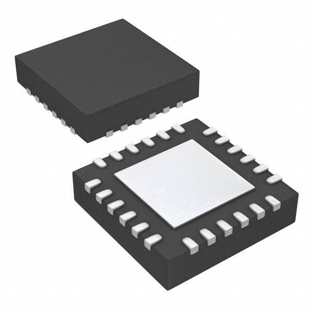


 工商网监
湘ICP备2023018690号
工商网监
湘ICP备2023018690号
