Product
Folder
Order
Now
Support &
Community
Tools &
Software
Technical
Documents
Reference
Design
TMP112
SBOS473I – MARCH 2009 – REVISED DECEMBER 2018
TMP112x High-Accuracy, Low-Power, Digital Temperature Sensors With SMBus and TwoWire Serial Interface in SOT563
1 Features
3 Description
•
The TMP112 family of devices are digital temperature
sensors designed for high-accuracy, low-power,
NTC/PTC thermistor replacements where high
accuracy is required. The TMP112A and TMP112B
offers 0.5°C accuracy and are optimized to provide
the best PSR performance for 3.3V and 1.8V
operation respectively, while TMP112N offers 1°C
accuracy. These temperature sensors are highly
linear and do not require complex calculations or
lookup tables to derive the temperature. The on-chip
12-bit ADC offers resolutions down to 0.0625°C.
1
•
•
•
•
•
•
•
•
TMP112A Accuracy Without Calibration :
– 0.5°C (Maximum) From 0°C to +65°C (3.3 V)
– 1.0°C (Maximum) From –40°C to +125°C
TMP112B Accuracy Without Calibration :
– 0.5°C (Maximum) From 0°C to +65°C (1.8 V)
– 1.0°C (Maximum) From –40°C to +125°C
TMP112N Accuracy Without Calibration:
– 1.0°C (Maximum) From –40°C to +125°C
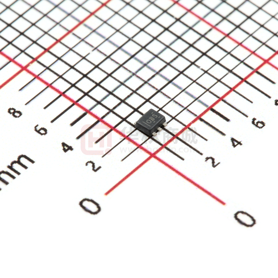
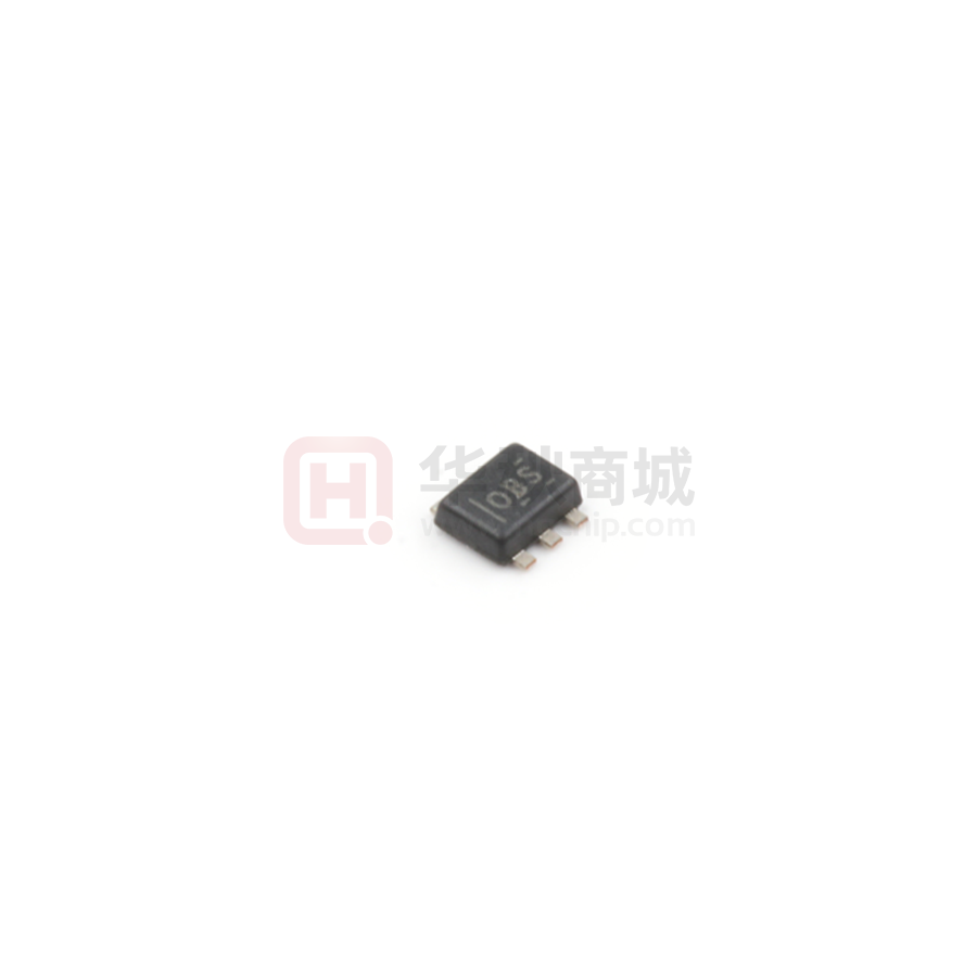
SOT563 Package (1.6 mm × 1.6 mm)
Low Quiescent Current:
– 10-μA Active (Maximum), 1-μA Shutdown
(Maximum)
Supply Range: 1.4 V to 3.6 V
Resolution: 12 Bits
Digital Output: SMBus™, Two-Wire, and I2C
Interface Compatibility
NIST Traceable
2 Applications
•
•
•
•
•
•
•
•
•
Portable and Battery-Powered Applications
Power-Supply Temperature Monitoring
Computer Peripheral Thermal Protection
Notebook Computers
Battery Management
Office Machines
Thermostat Controls
Electromechanical Device Temperatures
General Temperature Measurements:
– Industrial Controls
– Test Equipment
– Medical Instrumentation
The 1.6-mm × 1.6-mm SOT563 package is 68%
smaller footprint than an SOT23 package. The
TMP112 family features SMBus, two-wire and I2C
interface compatibility, and allows up to four devices
on one bus. The device also features an SMBus alert
function. The device is specified to operate over
supply voltages from 1.4 to 3.6 V with the maximum
quiescent current of 10 µA over the full operating
range.
The TMP112 family is designed for extended
temperature
measurement
in
communication,
computer, consumer, environmental, industrial, and
instrumentation applications. The device is specified
for operation over a temperature range of –40°C to
+125°C.
The TMP112 family production units are 100% tested
against sensors that are NIST-traceable and are
verified with equipment that are NIST-traceable
through ISO/IEC 17025 accredited calibrations.
Device Information(1)
PART NUMBER
TMP112x
PACKAGE
SOT563 (6)
BODY SIZE (NOM)
1.60 mm × 1.20 mm
(1) For all available packages, see the orderable addendum at
the end of the data sheet.
Block Diagram
Temperature
SCL
GND
ALERT
1
2
3
Diode
Temp.
Sensor
Control
Logic
6
DS
A/D
Converter
Serial
Interface
5
OSC
Config.
and Temp.
Register
4
SDA
V+
ADD0
TMP112
1
An IMPORTANT NOTICE at the end of this data sheet addresses availability, warranty, changes, use in safety-critical applications,
intellectual property matters and other important disclaimers. PRODUCTION DATA.
�TMP112
SBOS473I – MARCH 2009 – REVISED DECEMBER 2018
www.ti.com
Table of Contents
1
2
3
4
5
6
7
Features ..................................................................
Applications ...........................................................
Description .............................................................
Revision History.....................................................
Pin Configuration and Functions .........................
Specifications.........................................................
1
1
1
2
3
5
6.1
6.2
6.3
6.4
6.5
6.6
6.7
5
5
5
5
6
7
8
Absolute Maximum Ratings .....................................
ESD Ratings..............................................................
Recommended Operating Conditions.......................
Thermal Information ..................................................
Electrical Characteristics...........................................
Timing Requirements ................................................
Typical Characteristics ..............................................
Detailed Description ............................................ 10
7.1 Overview ................................................................. 10
7.2 Functional Block Diagrams ..................................... 10
7.3 Feature Description................................................. 11
7.4 Device Functional Modes........................................ 18
7.5 Programming .......................................................... 19
8
Application and Implementation ........................ 23
8.1 Application Information............................................ 23
8.2 Typical Application ................................................. 23
9 Power Supply Recommendations...................... 24
10 Layout................................................................... 25
10.1 Layout Guidelines ................................................. 25
10.2 Layout Example .................................................... 25
11 Device and Documentation Support ................. 26
11.1
11.2
11.3
11.4
11.5
Documentation Support .......................................
Community Resources..........................................
Trademarks ...........................................................
Electrostatic Discharge Caution ............................
Glossary ................................................................
26
26
26
26
26
12 Mechanical, Packaging, and Orderable
Information ........................................................... 26
4 Revision History
NOTE: Page numbers for previous revisions may differ from page numbers in the current version.
Changes from Revision H (October 2018) to Revision I
Page
•
Changed input voltage maximum to voltage maximum for SCL, ADD0 and SDA pins ......................................................... 5
•
Deleted Absolute Maximum Ratings for output voltage and replaced with pin level information........................................... 5
•
Added voltage at ALERT pin Absolute Maximum Ratings .................................................................................................... 5
Changes from Revision G (May 2018) to Revision H
Page
•
Added content to the ADD0 pin description in the Pin Functions table ................................................................................. 3
•
Changed the supply voltage maximum value in the Absolute Maximum Ratings table from: 5 V to: 4 V ............................. 5
•
Changed input voltage maximum value for the SCL, ADD0, and SDA pins in the Absolute Maximum Ratings table
from: 5 V to: 4 V ..................................................................................................................................................................... 5
•
Changed input voltage maximum value for the ALERT pin in the Absolute Maximum Ratings table from: (V+) + 0.5
V to: ((V+) + 0.5) and ≤ 4 V .................................................................................................................................................... 5
•
Changed Junction-to-ambient thermal resistance from 200 °C/W to 210.3 °C/W ................................................................ 5
•
Changed Junction-to-case (top) thermal resistance from 73.7 °C/W to 105.0 °C/W ............................................................ 5
•
Changed Junction-to-board thermal resistance from 34.4 °C/W to 87.5 °C/W ..................................................................... 5
•
Changed Junction-to-top characterization parameter from 3.1 °C/W to 6.1 °C/W ................................................................ 5
•
Changed Junction-to-board characterization parameter from 34.2 °C/W to 87.0 °C/W ........................................................ 5
Changes from Revision F (February 2018) to Revision G
Page
•
Changed long-term stability parameter to long-term drift ...................................................................................................... 6
•
Changed long-term drift test condition from: 3000 hours to: 3000 hours at 125°C................................................................ 6
•
Changed long-term drift typical value from: < 1 LSB to: ±0.0625°C ...................................................................................... 6
2
Submit Documentation Feedback
Copyright © 2009–2018, Texas Instruments Incorporated
Product Folder Links: TMP112
�TMP112
www.ti.com
SBOS473I – MARCH 2009 – REVISED DECEMBER 2018
Changes from Revision E (December 2015) to Revision F
Page
•
Added TMP112N and TMP112B orderables to the data sheet.............................................................................................. 1
•
Removed duplicate specified and operating temperature ranges from the Electrical Characteristics table .......................... 6
•
Removed Calibrating for Improved Accuracy and Using the Slope Specifications With a 1-Point Calibration sections...... 23
Changes from Revision D (April 2015) to Revision E
Page
•
Added TI Design .................................................................................................................................................................... 1
•
Added NIST Features bullet .................................................................................................................................................. 1
•
Added last paragraph to Description section ......................................................................................................................... 1
Changes from Revision C (October 2014) to Revision D
Page
•
Changed MIN, TYP, and MAX values for the Temperature Accuracy (temperature error) parameter .................................. 6
•
Changed the frequency from 2.85 to 3.4 MHz in the POWER SUPPLY section of the Electrical Characteristics table ...... 6
•
Changed the Temperature Error at 25°C graph in the Typical Characteristics section ......................................................... 8
•
Changed the Temperature Error vs Temperature graph in the Typical Characteristics section ............................................ 8
Changes from Revision B (June 2009) to Revision C
Page
•
Added Handling Rating table, Feature Description section, Device Functional Modes, Application and
Implementation section, Power Supply Recommendations section, Layout section, Device and Documentation
Support section, and Mechanical, Packaging, and Orderable Information section ............................................................... 5
•
Changed parameters in Timing Requirements ...................................................................................................................... 7
Changes from Revision A (March 2009) to Revision B
Page
•
Changed footnote 1 of Specifications for User-Calibrated Systems table .......................................................................... 23
•
Clarified Example 1; extended worst-case accuracy to be from –15°C to +50°C................................................................ 23
•
Changed equation in Using the Slope Specifications With a 1-Point Calibration ................................................................ 23
5 Pin Configuration and Functions
DRL Package
6-Pin SOT563
Top View
1
GND
2
ALERT
3
OBS
SCL
6
SDA
5
V+
4
ADD0
Pin Functions
PIN
NO.
NAME
I/O
DESCRIPTION
1
SCL
I
2
GND
—
Serial clock. Open-drain output; requires a pullup resistor.
Ground
3
ALERT
O
Overtemperature alert. Open-drain output; requires a pullup resistor.
4
ADD0
I
Address Select. Connect to V+, GND, SDA or SCL
Submit Documentation Feedback
Copyright © 2009–2018, Texas Instruments Incorporated
Product Folder Links: TMP112
3
�TMP112
SBOS473I – MARCH 2009 – REVISED DECEMBER 2018
www.ti.com
Pin Functions (continued)
PIN
NO.
NAME
I/O
5
V+
I
6
SDA
I/O
4
DESCRIPTION
Supply voltage, 1.4 V to 3.6 V
Serial data. Open-drain output; requires a pullup resistor.
Submit Documentation Feedback
Copyright © 2009–2018, Texas Instruments Incorporated
Product Folder Links: TMP112
�TMP112
www.ti.com
SBOS473I – MARCH 2009 – REVISED DECEMBER 2018
6 Specifications
6.1 Absolute Maximum Ratings
over operating free-air temperature range (unless otherwise noted) (1)
MIN
MAX
UNIT
4
V
–0.5
4
V
Voltage at ALERT
–0.5
((V+) + 0.3) and
≤4
V
Operating temperature
–55
150
°C
150
°C
150
°C
Supply voltage
V+
Voltage at SCL, ADD0, and SDA
Junction temperature, TJ
Storage temperature, Tstg
(1)
–60
Stresses beyond those listed under Absolute Maximum Ratings may cause permanent damage to the device. These are stress ratings
only, which do not imply functional operation of the device at these or any other conditions beyond those indicated under Recommended
Operating Conditions. Exposure to absolute-maximum-rated conditions for extended periods may affect device reliability.
6.2 ESD Ratings
VALUE
V(ESD)
(1)
(2)
Electrostatic discharge
Human body model (HBM), per ANSI/ESDA/JEDEC JS-001 (1)
±2000
Charged device model (CDM), per JEDEC specification JESD22-C101 (2)
±1000
UNIT
V
JEDEC document JEP155 states that 500-V HBM allows safe manufacturing with a standard ESD control process.
JEDEC document JEP157 states that 250-V CDM allows safe manufacturing with a standard ESD control process.
6.3 Recommended Operating Conditions
over operating free-air temperature range (unless otherwise noted)
MIN
NOM
MAX
V+
Supply voltage
1.4
3.3
3.6
UNIT
V
TA
Operating free-air temperature
–40
125
°C
6.4 Thermal Information
TMP112
THERMAL METRIC (1)
DRL (SOT563)
UNIT
6 PINS
RθJA
Junction-to-ambient thermal resistance
210.3
°C/W
RθJC(top)
Junction-to-case (top) thermal resistance
105.0
°C/W
RθJB
Junction-to-board thermal resistance
87.5
°C/W
ψJT
Junction-to-top characterization parameter
6.1
°C/W
ψJB
Junction-to-board characterization parameter
87.0
°C/W
RθJC(bot)
Junction-to-case (bottom) thermal resistance
N/A
°C/W
(1)
For more information about traditional and new thermal metrics, see the IC Package Thermal Metrics application report.
Submit Documentation Feedback
Copyright © 2009–2018, Texas Instruments Incorporated
Product Folder Links: TMP112
5
�TMP112
SBOS473I – MARCH 2009 – REVISED DECEMBER 2018
www.ti.com
6.5 Electrical Characteristics
At TA = +25°C and VS = +1.4V to +3.6V, unless otherwise noted.
PARAMETER
TEST CONDITIONS
MIN
TYP
MAX
UNIT
+125
°C
TEMPERATURE INPUT
Temperature range
–40
+25°C, V+ = 3.3 V
TMP112A
Accuracy
(temperature
error)
TMP112B
0°C to +65°C, V+ = 3.3 V
DC power-supply sensitivity
Long-term drift
(1)
±0.5
±0.25
±0.5
–40°C to +125°C
±0.5
±1
+25°C, V+ = 1.8 V
±0.1
±0.5
±0.25
±0.5
±0.5
±1
0.0625
±0.25
0°C to +65°C, V+ = 1.8 V
–40°C to +125°C
TMP112N
±0.1
–40°C to +125°C
°C
±1
–40°C to +125°C
3000 hours at 125°C
Resolution (LSB)
°C/V
±0.0625
°C
0.0625
°C
DIGITAL INPUT/OUTPUT
Input capacitance
VIH
3
Input logic level
VIL
IIN
Input current
VOL SDA
Output logic level
VOL ALERT
pF
0.7 (V+)
3.6
–0.5
0.3 (V+)
0 < VIN < 3.6 V
1
V+ > 2 V, IOL = 3 mA
0
0.4
V+ < 2 V, IOL = 3 mA
0
0.2 (V+)
V+ > 2 V, IOL = 3 mA
0
0.4
V+ < 2 V, IOL = 3 mA
0
0.2 (V+)
Resolution
12
Conversion time
26
Conversion modes
CR1 = 0, CR0 = 0
0.25
CR1 = 0, CR0 = 1
1
CR1 = 1, CR0 = 0 (default)
4
CR1 = 1, CR0 = 1
8
Timeout time
V
μA
V
V
Bits
35
ms
Conv/s
30
40
ms
POWER SUPPLY
Operating supply range
+1.4
Serial bus inactive, CR1 = 1, CR0 = 0
(default)
IQ
ISD
(1)
6
Average quiescent current
Shutdown current
+3.6
7
Serial bus active, SCL frequency = 400 kHz
15
Serial bus active, SCL frequency = 3.4 MHz
85
Serial bus inactive
0.5
Serial bus active, SCL frequency = 400 kHz
10
Serial bus active, SCL frequency = 3.4 MHz
80
V
10
μA
1
μA
Long-term drift is determined using accelerated operational life testing at a junction temperature of 150°C for 1000 hours.
Submit Documentation Feedback
Copyright © 2009–2018, Texas Instruments Incorporated
Product Folder Links: TMP112
�TMP112
www.ti.com
SBOS473I – MARCH 2009 – REVISED DECEMBER 2018
6.6 Timing Requirements
See the Two-Wire Timing Diagrams section for timing diagrams.
FAST MODE
V+
HIGH-SPEED
MODE
MIN
MAX
MIN
MAX
0.001
0.4
0.001
2.85
UNIT
ƒ(SCL)
SCL operating frequency
t(BUF)
Bus-free time between STOP and START
condition
600
160
ns
t(HDSTA)
Hold time after repeated START condition.
After this period, the first clock is generated.
600
160
ns
t(SUSTA)
repeated start condition setup time
600
160
ns
t(SUSTO)
STOP condition setup time
600
t(HDDAT)
Data hold time
100
t(SUDAT)
Data setup time
100
25
ns
t(LOW)
SCL-clock low period
V+ , see Figure 10
1300
210
ns
t(HIGH)
SCL-clock high period
See Figure 10
600
60
tFD
Data fall time
See Figure 10
tRD
Data rise time
tFC
Clock fall time
See Figure 10
300
40
ns
tRC
Clock rise time
See Figure 10
300
40
ns
See Figure 10
See Figure 10
SCLK ≤ 100 kHz, see Figure 10
160
900
300
25
ns
105
Product Folder Links: TMP112
ns
ns
80
300
ns
ns
1000
ns
Submit Documentation Feedback
Copyright © 2009–2018, Texas Instruments Incorporated
MHz
7
�TMP112
SBOS473I – MARCH 2009 – REVISED DECEMBER 2018
www.ti.com
6.7 Typical Characteristics
At TA = +25°C and V+ = 3.3 V, unless otherwise noted.
30
25
Population
Population
20
15
10
-0.250
-0.225
-0.200
-0.175
-0.150
-0.125
-0.100
-0.075
-0.050
-0.025
0
0.025
0.050
0.075
0.100
0.125
0.150
0.175
0.200
0.225
0.250
0.3
0.35
0.2
0.25
0.1
0.15
0
0.05
-0.1
-0.05
-0.2
-0.15
-0.3
-0.25
0
-0.35
5
D001
Accuracy vs Supply (°C/V)
Temperature Error (qC)
Figure 2. Accuracy vs Supply
1
20
0.8
18
0.6
16
14
0.4
IQ (µA)
Temperature Error (qC)
Figure 1. Temperature Error at 25°C
0.2
0
10
3.6V Supply
8
-0.2
6
-0.4
4
-0.6
Mean
Mean + 3 V
Mean 3 V
-0.8
-1
-60
-40
-20
0
0
-60
20
40
60
80
Temperature (qC)
100
120
0
D002
90
8
80
7
70
6
60
100 120 140 160
+125°C
30
1.4V Supply
80
50
40
3
60
Figure 4. Average Quiescent Current vs Temperature
100
4
40
Four Conversions
per Second
9
3.6V Supply
20
Temperature (°C)
10
5
-40 -20
140
IQ (µA)
ISD (µA)
1.4V Supply
2
Figure 3. Temperature Error vs Temperature
2
20
1
10
+25°C
-55°C
0
0
-60
8
12
-40 -20
0
20
40
60
80
100 120 140 160
1k
10k
100k
1M
10M
Temperature (°C)
Bus Frequency (Hz)
Figure 5. Shutdown Current vs Temperature
Figure 6. Quiescent Current vs Bus Frequency
(Temperature at 3.3-V Supply)
Submit Documentation Feedback
Copyright © 2009–2018, Texas Instruments Incorporated
Product Folder Links: TMP112
�TMP112
www.ti.com
SBOS473I – MARCH 2009 – REVISED DECEMBER 2018
Typical Characteristics (continued)
At TA = +25°C and V+ = 3.3 V, unless otherwise noted.
40
Conversion Time (ms)
38
36
34
32
1.4V Supply
30
28
26
3.6V Supply
24
22
20
-60
-40 -20
0
20
40
60
80
100 120 140 160
Temperature (°C)
Figure 7. Conversion Time vs Temperature
Submit Documentation Feedback
Copyright © 2009–2018, Texas Instruments Incorporated
Product Folder Links: TMP112
9
�TMP112
SBOS473I – MARCH 2009 – REVISED DECEMBER 2018
www.ti.com
7 Detailed Description
7.1 Overview
The TMP112 family of devices are digital temperature sensors that are optimal for thermal-management and
thermal-protection applications. The TMP112 family is two-wire, SMBus, and I2C interface-compatible. The
device is specified over an operating temperature range of –40°C to 125°C. Figure 8 shows a block diagram of
the TMP112 family. Figure 9 shows the ESD protection circuitry contained in the TMP112 family.
The temperature sensor in the TMP112 family is the chip itself. Thermal paths run through the package leads as
well as the plastic package. The package leads provide the primary thermal path because of the lower thermal
resistance of the metal.
An alternative version of the TMP112 family is available. The TMP102 device has reduced accuracy, the same
micro-package, and is pin-to-pin compatible.
Table 1. Advantages of TMP112 family Versus TMP102
DEVICE
COMPATIBLE
INTERFACES
PACKAGE
SUPPLY
CURRENT
SUPPLY
VOLTAGE
(MIN)
SUPPLY
VOLTAGE
(MAX)
RESOLUTION
LOCAL SENSOR
ACCURACY (MAX)
SPECIFIED
CALIBRATION
DRIFT SLOPE
TMP112
family
I2C
SMBus
SOT563
1.2 × 1.6 × 0.6
10 µA
1.4 V
3.6 V
12 Bit
0.0625°C
0.5°C: (0°C to 65°C)
1°C: (-40°C to 125°C)
Yes
TMP102
I2C
SMBus
SOT563
1.2 × 1.6 × 0.6
10 µA
1.4 V
3.6 V
12 Bit
0.0625°C
2°C: (25°C to 85°C)
3°C: (-40°C to 125°C)
No
7.2 Functional Block Diagrams
Temperature
SCL
GND
ALERT
1
2
3
Diode
Temp.
Sensor
Control
Logic
6
DS
A/D
Converter
Serial
Interface
5
OSC
Config.
and Temp.
Register
SDA
V+
4
ADD0
TMP112
Figure 8. Internal Block Diagram
10
Submit Documentation Feedback
Copyright © 2009–2018, Texas Instruments Incorporated
Product Folder Links: TMP112
�TMP112
www.ti.com
SBOS473I – MARCH 2009 – REVISED DECEMBER 2018
Functional Block Diagrams (continued)
TMP112
SCL
SDA
V+
GND
Core
V+
ALERT
A0
Figure 9. Equivalent Internal ESD Circuitry
7.3 Feature Description
7.3.1 Digital Temperature Output
The digital output from each temperature measurement conversion is stored in the read-only temperature
register. The temperature register of the TMP112 family is configured as a 12-bit read-only register (setting the
EM bit to 0 in the configuration register; see the Extended Mode (EM) section), or as a 13-bit read-only register
(setting the EM bit to 1 in the configuration register) that stores the output of the most recent conversion. Two
bytes must be read to obtain data and are listed in Table 8 and Table 9. Byte 1 is the most significant byte
(MSB), followed by byte 2, the least significant byte (LSB). The first 12 bits (13 bits in extended mode) are used
to indicate temperature. The least significant byte does not have to be read if that information is not needed. The
data format for temperature is listed in Table 2 and Table 3. One LSB equals 0.0625°C. Negative numbers are
represented in binary twos complement format. Following power up or reset, the temperature register reads 0°C
until the first conversion is complete. Bit D0 of byte 2 indicates normal mode (EM bit equals 0) or extended mode
(EM bit equals 1), and can be used to distinguish between the two temperature register data formats. The
unused bits in the temperature register always read 0.
Table 2. 12-Bit Temperature Data Format (1)
(1)
TEMPERATURE (°C)
DIGITAL OUTPUT (BINARY)
HEX
128
0111 1111 1111
7FF
127.9375
0111 1111 1111
7FF
100
0110 0100 0000
640
80
0101 0000 0000
500
75
0100 1011 0000
4B0
50
0011 0010 0000
320
25
0001 1001 0000
190
0.25
0000 0000 0100
004
0
0000 0000 0000
000
–0.25
1111 1111 1100
FFC
–25
1110 0111 0000
E70
–55
1100 1001 0000
C90
The resolution for the Temperature ADC in Internal Temperature mode is 0.0625°C/count.
Submit Documentation Feedback
Copyright © 2009–2018, Texas Instruments Incorporated
Product Folder Links: TMP112
11
�TMP112
SBOS473I – MARCH 2009 – REVISED DECEMBER 2018
www.ti.com
Table 2 does not list all temperatures. Use the following rules to obtain the digital data format for a given
temperature or the temperature for a given digital data format.
To convert positive temperatures to a digital data format:
1. Divide the temperature by the resolution
2. Convert the result to binary code with a 12-bit, left-justified format, and MSB = 0 to denote a positive sign.
Example: (50°C) / (0.0625°C / LSB) = 800 = 320h = 0011 0010 0000
To convert a positive digital data format to temperature:
1. Convert the 12-bit, left-justified binary temperature result, with the MSB = 0 to denote a positive sign, to a
decimal number.
2. Multiply the decimal number by the resolution to obtain the positive temperature.
Example: 0011 0010 0000 = 320h = 800 × (0.0625°C / LSB) = 50°C
To convert negative temperatures to a digital data format:
1. Divide the absolute value of the temperature by the resolution, and convert the result to binary code with a
12-bit, left-justified format.
2. Generate the twos complement of the result by complementing the binary number and adding one. Denote a
negative number with MSB = 1.
Example: (|–25°C|) / (0.0625°C / LSB) = 400 = 190h = 0001 1001 0000
Two's complement format: 1110 0110 1111 + 1 = 1110 0111 0000
To convert a negative digital data format to temperature:
1. Generate the twos compliment of the 12-bit, left-justified binary number of the temperature result (with MSB
= 1, denoting negative temperature result) by complementing the binary number and adding one. This
represents the binary number of the absolute value of the temperature.
2. Convert to decimal number and multiply by the resolution to get the absolute temperature, then multiply by
–1 for the negative sign.
Example: 1110 0111 0000 has twos compliment of 0001 1001 0000 = 0001 1000 1111 + 1
Convert to temperature: 0001 1001 0000 = 190h = 400; 400 × (0.0625°C / LSB) = 25°C = (|–25°C|);
(|–25°C|) × (–1) = –25°C
Table 3. 13-Bit Temperature Data Format
12
TEMPERATURE (°C)
DIGITAL OUTPUT (BINARY)
HEX
150
0 1001 0110 0000
0960
128
0 1000 0000 0000
0800
127.9375
0 0111 1111 1111
07FF
100
0 0110 0100 0000
0640
80
0 0101 0000 0000
0500
75
0 0100 1011 0000
04B0
50
0 0011 0010 0000
0320
25
0 0001 1001 0000
0190
0.25
0 0000 0000 0100
0004
0
0 0000 0000 0000
0000
–0.25
1 1111 1111 1100
1FFC
–25
1 1110 0111 0000
1E70
–55
1 1100 1001 0000
1C90
Submit Documentation Feedback
Copyright © 2009–2018, Texas Instruments Incorporated
Product Folder Links: TMP112
�TMP112
www.ti.com
SBOS473I – MARCH 2009 – REVISED DECEMBER 2018
7.3.2 Serial Interface
The TMP112 family operates as a slave device only on the SMBus, two-wire, and I2C interface-compatible bus.
Connections to the bus are made through the open-drain I/O lines, SDA and SCL. The SDA and SCL pins
feature integrated spike suppression filters and Schmitt triggers to minimize the effects of input spikes and bus
noise. The TMP112 family supports the transmission protocol for both fast (1 kHz to 400 kHz) and high-speed (1
kHz to 2.85 MHz) modes. All data bytes are transmitted MSB first..
7.3.2.1 Bus Overview
The device that initiates the transfer is called a master, and the devices controlled by the master are slaves. The
bus must be controlled by a master device that generates the serial clock (SCL), controls the bus access, and
generates the START and STOP conditions.
To address a specific device, a START condition is initiated, indicated by pulling the data-line (SDA) from a highto low-logic level when the SCL pin is high. All slaves on the bus shift in the slave address byte on the rising
edge of the clock, with the last bit indicating whether a read or write operation is intended. During the ninth clock
pulse, the slave being addressed responds to the master by generating an acknowledge and pulling the SDA pin
low.
A data transfer is then initiated and sent over eight clock pulses followed by an acknowledge bit. During the data
transfer the SDA pin must remain stable when the SCL pin is high, because any change in the SDA pin when the
SCL pin is high is interpreted as a START or STOP signal.
When all data have been transferred, the master generates a STOP condition indicated by pulling the SDA pin
from low to high when the SCL pin is high.
7.3.2.2 Serial Bus Address
To communicate with the device, the master must first address slave devices through a slave-address byte. The
slave-address byte consists of seven address bits and a direction bit indicating the intent of executing a read or
write operation.
The TMP112 family features an address pin to allow up to four devices to be addressed on a single bus. Table 4
describes the pin logic levels used to properly connect up to four devices.
Table 4. Address Pin and Slave Addresses
DEVICE TWO-WIRE ADDRESS
A0 PIN CONNECTION
1001000
Ground
1001001
V+
1001010
SDA
1001011
SCL
7.3.2.3 Writing and Reading Operation
Accessing a particular register on the TMP112 family is accomplished by writing the appropriate value to the
pointer register. The value for the pointer register is the first byte transferred after the slave address byte with the
R/W bit low. Every write operation to the TMP112 family requires a value for the pointer register (see Figure 11).
When reading from the TMP112 family, the last value stored in the pointer register by a write operation is used to
determine which register is read by a read operation. To change the register pointer for a read operation, a new
value must be written to the pointer register. This action is accomplished by issuing a slave-address byte with the
R/W bit low, followed by the pointer register byte. No additional data are required. The master can then generate
a START condition and send the slave address byte with the R/W bit high to initiate the read command. See
Figure 12 for details of this sequence. If repeated reads from the same register are desired, continuously sending
the pointer register bytes is not necessary because the TMP112 family retains the pointer register value until the
value is changed by the next write operation.
Register bytes are sent with the most significant byte first, followed by the least significant byte.
Submit Documentation Feedback
Copyright © 2009–2018, Texas Instruments Incorporated
Product Folder Links: TMP112
13
�TMP112
SBOS473I – MARCH 2009 – REVISED DECEMBER 2018
www.ti.com
7.3.2.4 Slave Mode Operations
The TMP112 family can operate as a slave receiver or slave transmitter. As a slave device, the TMP112 family
never drives the SCL line.
7.3.2.4.1 Slave Receiver Mode
The first byte transmitted by the master is the slave address with the R/W bit low. The TMP112 family then
acknowledges reception of a valid address. The next byte transmitted by the master is the pointer register. The
TMP112 family then acknowledges reception of the pointer register byte. The next byte or bytes are written to the
register addressed by the pointer register. The TMP112 family acknowledges reception of each data byte. The
master can terminate data transfer by generating a START or STOP condition.
7.3.2.4.2 Slave Transmitter Mode
The first byte transmitted by the master is the slave address with the R/W bit high. The slave acknowledges
reception of a valid slave address. The next byte is transmitted by the slave and is the most significant byte of
the register indicated by the pointer register. The master acknowledges reception of the data byte. The next byte
transmitted by the slave is the least significant byte. The master acknowledges reception of the data byte. The
master can terminate data transfer by generating a not-acknowledge on reception of any data byte or by
generating a START or STOP condition.
7.3.2.5 SMBus Alert Function
The TMP112 family supports the SMBus alert function. When the TMP112 family operates in interrupt mode (TM
= 1), the ALERT pin can be connected as an SMBus alert signal. When a master senses that an alert condition
is present on the alert line, the master sends an SMBus ALERT command (0001 1001) to the bus. If the ALERT
pin is active, the device acknowledges the SMBus ALERT command and responds by returning the slave
address on the SDA line. The eighth bit (LSB) of the slave address byte indicates if the alert condition is caused
by the temperature exceeding T(HIGH) or falling below T(LOW). The LSB is high if the temperature is greater than
T(HIGH), or low if the temperature is less than T(LOW). Refer to the Figure 13 section for details of this sequence.
If multiple devices on the bus respond to the SMBus ALERT command, arbitration during the slave address
portion of the SMBus ALERT command determines which device clears the alert status of that device. The
device with the lowest two-wire address wins the arbitration. If the TMP112 family wins the arbitration, the
TMP112 family ALERT pin becomes inactive at the completion of the SMBus ALERT command. If the TMP112
family loses the arbitration, the TMP112 family ALERT pin remains active.
7.3.2.6 General Call
The TMP112 family responds to a two-wire general-call address (0000 000) if the eighth bit is 0. The device
acknowledges the general-call address and responds to commands in the second byte. If the second byte is
0000 0110, the TMP112 family internal registers are reset to power-up values. The TMP112 family does not
support the general-address acquire command.
7.3.2.7 High-Speed (Hs) Mode
For the two-wire bus to operate at frequencies above 400 kHz, the master device must issue an Hs-mode master
code (0000 1xxx) as the first byte after a START condition to switch the bus to high-speed operation. The
TMP112 family does not acknowledge this byte, but switches the input filters on the SDA and SCL pins and the
output filters on the SDA pin to operate in Hs-mode, thus allowing transfers at up to 2.85 MHz. After the Hsmode master code has been issued, the master transmits a two-wire slave address to initiate a data-transfer
operation. The bus continues to operate in Hs-mode until a STOP condition occurs on the bus. Upon receiving
the STOP condition, the TMP112 family switches the input and output filters back to fast-mode operation.
7.3.2.8 Timeout Function
The TMP112 family resets the serial interface if the SCL pin is held low for 30 ms (typical) between a start and
stop condition. The TMP112 family releases the SDA line if the SCL pin is pulled low and waits for a start
condition from the host controller. To avoid activating the timeout function, maintain a communication speed of at
least 1 kHz for SCL operating frequency.
14
Submit Documentation Feedback
Copyright © 2009–2018, Texas Instruments Incorporated
Product Folder Links: TMP112
�TMP112
www.ti.com
SBOS473I – MARCH 2009 – REVISED DECEMBER 2018
7.3.2.9 Timing Diagrams
The TMP112 family is two-wire, SMBus and I2C interface-compatible. Figure 10 to Figure 13 describe the various
operations on the TMP112 family. Parameters for Figure 10 are defined in Timing Requirements. Bus definitions
are:
Bus Idle: Both SDA and SCL lines remain high.
Start Data Transfer: A change in the state of the SDA line, from high to low, when the SCL line is high, defines
a START condition. Each data transfer is initiated with a START condition.
Stop Data Transfer: A change in the state of the SDA line from low to high when the SCL line is high defines a
STOP condition. Each data transfer is terminated with a repeated START or STOP condition.
Data Transfer: The number of data bytes transferred between a START and a STOP condition is not limited and
is determined by the master device. The TMP112 family can also be used for single byte updates. To update
only the MS byte, terminate the communication by issuing a START or STOP communication on the bus.
Acknowledge: Each receiving device, when addressed, is obliged to generate an Acknowledge bit. A device
that acknowledges must pull down the SDA line during the Acknowledge clock pulse in such a way that the SDA
line is stable low during the high period of the Acknowledge clock pulse. Setup and hold times must be taken into
account. On a master receive, the termination of the data transfer can be signaled by the master generating a
Not-Acknowledge ('1') on the last byte that has been transmitted by the slave.
7.3.2.9.1 Two-Wire Timing Diagrams
See the Timing Requirements.
t(LOW)
tFC
t(HDSTA)
tRC
SCL
t(HDSTA)
t(HIGH)
t(HDDAT)
t(SUSTO)
t(SUSTA)
t(SUDAT)
SDA
t(BUF)
P
tRD
tFD
S
S
P
Figure 10. Two-Wire Timing Diagram
Submit Documentation Feedback
Copyright © 2009–2018, Texas Instruments Incorporated
Product Folder Links: TMP112
15
�TMP112
SBOS473I – MARCH 2009 – REVISED DECEMBER 2018
www.ti.com
1
9
1
9
SCL
¼
1
SDA
0
0
1
0
A1(1)
A0(1)
R/W
Start By
Master
0
0
0
0
0
0
P1
P0
ACK By
TMP112
¼
ACK By
TMP112
Frame 2 Pointer Register Byte
Frame 1 Two-Wire Slave Address Byte
9
1
1
9
SCL
(Continued)
SDA
(Continued)
D7
D6
D5
D4
D3
D2
D1
D0
D7
D6
D5
D4
D3
D2
D1
D0
ACK By
TMP112
ACK By
TMP112
Stop By
Master
Frame 4 Data Byte 2
Frame 3 Data Byte 1
NOTE: (1) The values of A0 and A1 are determined by the ADD0 pin.
Figure 11. Two-Wire Timing Diagram for Write Word Format
16
Submit Documentation Feedback
Copyright © 2009–2018, Texas Instruments Incorporated
Product Folder Links: TMP112
�TMP112
www.ti.com
SBOS473I – MARCH 2009 – REVISED DECEMBER 2018
1
9
1
9
SCL
¼
SDA
1
0
0
1
0
A1
(1)
A0
(1)
R/W
Start By
Master
0
0
0
0
0
0
P1
P0
ACK By
TMP112
Stop By
Master
ACK By
TMP112
Frame 1 Two-Wire Slave Address Byte
Frame 2 Pointer Register Byte
1
9
1
9
SCL
(Continued)
¼
SDA
(Continued)
1
0
0
1
0
A1
(1)
A0
(1)
R/W
Start By
Master
D7
D6
D5
D4
D3
ACK By
TMP112
D1
D0
¼
ACK By
From
TMP112
Frame 3 Two-Wire Slave Address Byte
1
D2
Master
(2)
Frame 4 Data Byte 1 Read Register
9
SCL
(Continued)
SDA
(Continued)
D7
D6
D5
D4
D3
D2
D1
D0
From
TMP112
ACK By
Master
Stop By
Master
(3)
Frame 5 Data Byte 2 Read Register
NOTE: (1) The values of A0 and A1 are determined by the ADD0 pin.
(2) Master should leave SDA high to terminate a single-byte read operation.
(3) Master should leave SDA high to terminate a two-byte read operation.
Figure 12. Two-Wire Timing Diagram for Read Word Format
ALERT
1
9
1
9
SCL
SDA
0
0
0
1
1
Start By
Master
0
0
1
R/W
0
0
1
A1
ACK By
TMP112
Frame 1 SMBus ALERT Response Address Byte
A0
From
TMP112
Status
NACK By
Master
Stop By
Master
Frame 2 Slave Address From TMP112
NOTE: (1) The values of A0 and A1 are determined by the ADD0 pin.
Figure 13. Timing Diagram for SMBus ALERT
Submit Documentation Feedback
Copyright © 2009–2018, Texas Instruments Incorporated
Product Folder Links: TMP112
17
�TMP112
SBOS473I – MARCH 2009 – REVISED DECEMBER 2018
www.ti.com
7.4 Device Functional Modes
7.4.1 Continuos-Conversion Mode
The default mode of the TMP112 family is continuos conversion mode. During continuous-conversion mode, the
ADC performs continuos temperature conversions and stores each results to the temperature register,
overwriting the result from the previous conversion. The conversion rate bits, CR1 and CR0, configure the
TMP112 family for conversion rates of 0.25 Hz, 1 Hz, 4 Hz, or 8 Hz. The default rate is 4 Hz. The TMP112 family
has a typical conversion time of 26 ms. To achieve different conversion rates, the TMP112 family makes a
conversion and then powers down and waits for the appropriate delay set by CR1 and CR0. Table 5 lists the
settings for CR1 and CR0.
Table 5. Conversion Rate Settings
CR1
CR0
CONVERSION RATE
0
0
0.25 Hz
0
1
1 Hz
1
0
4 Hz (default)
1
1
8 Hz
After a power-up or general-call reset, the TMP112 family immediately begins a conversion as shown in
Figure 14. The first result is available after 26 ms (typical). The active quiescent current during conversion is 40
μA (typical at +27°C). The quiescent current during delay is 2.2 μA (typical at +27°C).
Delay
(1)
26ms
26ms
Startup
Start of
Conversion
(1) Delay is set by CR1 and CR0.
Figure 14. Conversion Start
7.4.2 Extended Mode (EM)
The extended mode bit configures the device for normal mode operation (EM = 0) or extended mode operation
(EM = 1). In normal mode, the temperature register and the high and low limit registers use a 12-bit data format.
Normal mode is used to make the TMP112 family compatible with the TMP75 device.
Extended mode (EM = 1) allows measurement of temperatures above 128°C by configuring the temperature
register and the high and low limit registers for 13-bit data format.
7.4.3 One-Shot/Conversion Ready Mode (OS)
The TMP112 family features a one-shot temperature-measurement mode. When the device is in shutdown
mode, writing a 1 to the OS bit begins a single temperature conversion. During the conversion, the OS bit reads
0. The device returns to the SHUTDOWN state at the completion of the single conversion. After the conversion,
the OS bit reads 1. This feature is useful for reducing power consumption in the TMP112 family when continuous
temperature monitoring is not required.
As a result of the short conversion time, the TMP112 family can achieve a higher conversion rate. A single
conversion typically occurs for 26 ms and a read can occur in less than 20 μs. When using one-shot mode, 30 or
more conversions per second are possible.
7.4.4 Thermostat Mode (TM)
The thermostat mode bit indicates to the device whether to operate in comparator mode (TM = 0 ) or interrupt
mode (TM = 1).
18
Submit Documentation Feedback
Copyright © 2009–2018, Texas Instruments Incorporated
Product Folder Links: TMP112
�TMP112
www.ti.com
SBOS473I – MARCH 2009 – REVISED DECEMBER 2018
7.4.4.1 Comparator Mode (TM = 0)
In Comparator mode (TM = 0), the Alert pin is activated when the temperature equals or exceeds the value in the
T(HIGH) register and remains active until the temperature falls below the value in the T(LOW)register. For more
information on the comparator mode, see the High- and Low-Limit Register section.
7.4.4.2 Interrupt Mode (TM = 1)
In Interrupt mode (TM = 1), the Alert pin is activated when the temperature exceeds T(HIGH) or goes below T(LOW)
registers. The Alert pin is cleared when the host controller reads the temperature register. For more information
on the interrupt mode, see the High- and Low-Limit Register section.
7.5 Programming
7.5.1 Pointer Register
Figure 15 shows the internal register structure of the TMP112 family. The 8-bit Pointer Register of the device is
used to address a given data register. The Pointer Register uses the two LSBs (see Table 13) to identify which
of the data registers must respond to a read or write command. The power-up reset value of P1/P0 is '00'. By
default, the TMP112 family reads the temperature on power-up.
Pointer
Register
Temperature
Register
SCL
Configuration
Register
I/O
Control
Interface
TLOW
Register
SDA
THIGH
Register
Figure 15. Internal Register Structure
Table 6 lists the pointer address of the registers available in the TMP112 family. Table 7 lists the bits of the
Pointer Register byte. During a write command, bytes P2 through P7 must always be 0.
Table 6. Pointer Addresses
P1
P0
REGISTER
0
0
Temperature Register (Read Only)
0
1
Configuration Register (Read/Write)
1
0
TLOW Register (Read/Write)
1
1
THIGH Register (Read/Write)
Table 7. Pointer Register Byte
P7
P6
P5
P4
P3
P2
0
0
0
0
0
0
P1
P0
Register Bits
Submit Documentation Feedback
Copyright © 2009–2018, Texas Instruments Incorporated
Product Folder Links: TMP112
19
�TMP112
SBOS473I – MARCH 2009 – REVISED DECEMBER 2018
www.ti.com
7.5.2 Temperature Register
The Temperature Register of the TMP112 family is configured as a 12-bit read-only register (setting the EM bit to
0 in the configuration register; see the Extended Mode section), or as a 13-bit read-only register (setting the EM
bit to 1 in the configuration register) that stores the output of the most recent conversion. Two bytes must be
read to obtain data and are listed in Table 8 and Table 9. Byte 1 is the most significant byte (MSB), followed by
byte 2, the least significant byte (LSB). The first 12 bits (13 bits in extended mode) are used to indicate
temperature. The least significant byte does not have to be read if that information is not needed.
Table 8. Byte 1 of Temperature Register
BYTE
D7
1
D6
D5
D4
D3
D2
D1
D0
T11
T10
T9
T8
T7
T6
T5
T4
(T12)
(T11)
(T10)
(T9)
(T8)
(T7)
(T6)
(T5)
D0
Table 9. Byte 2 of Temperature Register (1)
BYTE
2
(1)
D7
D6
D5
D4
D3
D2
D1
T3
T2
T1
T0
0
0
0
0
(T4)
(T3)
(T2)
(T1)
(T0)
(0)
(0)
(1)
Extended mode 13-bit configuration shown in parentheses.
7.5.3 Configuration Register
The Configuration Register is a 16-bit read/write register used to store bits that control the operational modes of
the temperature sensor. Read/write operations are performed MSB first. Table 10 lists the format and power-up
and reset values of the configuration register. For compatibility, the first byte corresponds to the Configuration
Register in the TMP75 and TMP275 devices. All registers are updated byte by byte.
Table 10. Configuration and Power-Up/Reset Formats
BYTE
1
2
D7
D6
D5
D4
D3
D2
D1
D0
OS
R1
R0
F1
F0
POL
TM
SD
0
1
1
0
0
0
0
0
CR1
CR0
AL
EM
0
0
0
0
1
0
1
0
0
0
0
0
7.5.3.1 Shutdown Mode (SD)
The Shutdown mode bit saves maximum power by shutting down all device circuitry other than the serial
interface, reducing current consumption to typically less than 0.5 μA. Shutdown mode is enabled when the SD bit
= 1; the device shuts down when current conversion is completed. When SD = 0, the device maintains a
continuous conversion state.
7.5.3.2 Thermostat Mode (TM)
The Thermostat mode bit indicates to the device whether to operate in Comparator mode (TM = 0) or Interrupt
mode (TM = 1). For more information on Comparator and Interrupt modes, see the High- and Low-Limit
Registers section.
7.5.3.3 Polarity (POL)
The polarity bit allows the user to adjust the polarity of the ALERT pin output. If the POL bit is set to 0 (default),
the ALERT pin becomes active low . When the POL bit is set to 1, the ALERT pin becomes active high and the
state of the ALERT pin is inverted. The operation of the ALERT pin in various modes is illustrated in Figure 16.
20
Submit Documentation Feedback
Copyright © 2009–2018, Texas Instruments Incorporated
Product Folder Links: TMP112
�TMP112
www.ti.com
SBOS473I – MARCH 2009 – REVISED DECEMBER 2018
THIGH
Measured
Temperature
TLOW
SN1511004 ALERT PIN
(Comparator Mode)
POL = 0
SN1511004 ALERT PIN
(Interrupt Mode)
POL = 0
SN1511004 ALERT PIN
(Comparator Mode)
POL = 1
SN1511004 ALERT PIN
(Interrupt Mode)
POL = 1
Read
Read
Read
Time
Figure 16. Output Transfer Function Diagrams
7.5.3.4 Fault Queue (F1/F0)
A fault condition exists when the measured temperature exceeds the user-defined limits set in the THIGH and
TLOW registers. Additionally, the number of fault conditions required to generate an alert may be programmed
using the fault queue. The fault queue is provided to prevent a false alert as a result of environmental noise. The
fault queue requires consecutive fault measurements in order to trigger the alert function. Table 11 lists the
number of measured faults that may be programmed to trigger an alert condition in the device. For THIGH and
TLOW register format and byte order, see the High- and Low-Limit Registers section.
Table 11. TMP112 family Fault Settings
F1
F0
CONSECUTIVE FAULTS
0
0
1
0
1
2
1
0
4
1
1
6
7.5.3.5 Converter Resolution (R1 and R0)
The converter resolution bits, R1 and R0, are read-only bits. The TMP112 family converter resolution is set on
start up to 11 which sets the temperature register to a 12-bit resolution.
7.5.3.6 One-Shot (OS)
When the device is in shutdown mode, writing a 1 to the OS bit begins a single temperature conversion. During
the conversion, the OS bit reads 0. The device returns to the SHUTDOWN state at the completion of the single
conversion. For more information on the one-shot conversion mode, see the One-Shot/Conversion Ready Mode
(OS) section.
7.5.3.7 Extended Mode (EM)
The extended mode bit configures the device for normal mode operation (EM = 0) or extended mode operation
(EM = 1). In normal mode, the temperature register and the high and low limit registers use a 12-bit data format.
For more information on the extended mode, see the Extended Mode (EM) section.
Submit Documentation Feedback
Copyright © 2009–2018, Texas Instruments Incorporated
Product Folder Links: TMP112
21
�TMP112
SBOS473I – MARCH 2009 – REVISED DECEMBER 2018
www.ti.com
7.5.3.8 Alert (AL)
The AL bit is a read-only function. Reading the AL bit provides information about the comparator mode status.
The state of the POL bit inverts the polarity of data returned from the AL bit. When the POL bit equals 0, the AL
bit reads as 1 until the temperature equals or exceeds T(HIGH) for the programmed number of consecutive faults,
causing the AL bit to read as 0. The AL bit continues to read as 0 until the temperature falls below T(LOW) for the
programmed number of consecutive faults, when it again reads as 1. The status of the TM bit does not affect the
status of the AL bit.
7.5.4 High- and Low-Limit Register
The temperature limits are stored in the T(LOW) and T(HIGH) registers in the same format as the temperature result,
and their values are compared to the temperature result on every conversion. The outcome of the comparison
drives the behavior of the ALERT pin, which operates as a comparator output or an interrupt, and is set by the
TM bit in the configuration register.
In Comparator mode (TM = 0), the ALERT pin becomes active when the temperature equals or exceeds the
value in the T(HIGH) register and generates a consecutive number of faults according to fault bits F1 and F0. The
ALERT pin remains active until the temperature falls below the indicated T(LOW) value for the same number of
faults.
In interrupt mode (TM = 1), the ALERT pin becomes active when the temperature equals or exceeds the value in
T(HIGH) for a consecutive number of fault conditions (as shown in Table 11). The ALERT pin remains active until a
read operation of any register occurs, or the device successfully responds to the SMBus alert response address.
The ALERT pin is also cleared if the device is placed in shutdown mode. When the ALERT pin is cleared, it
becomes active again only when temperature falls below T(LOW), and remains active until cleared by a read
operation of any register or a successful response to the SMBus alert response address. When the ALERT pin is
cleared, the above cycle repeats, with the ALERT pin becoming active when the temperature equals or exceeds
T(HIGH). The ALERT pin can also be cleared by resetting the device with the general-call Reset command. This
action also clears the state of the internal registers in the device, returning the device to comparator mode
(TM = 0).
Both operating modes are represented in Figure 16. Table 12 and Table 13 list the format for the THIGH and TLOW
registers. The most significant byte is sent first, followed by the least significant byte. The power-up reset values
for T(HIGH) and T(LOW) are:
• THIGH = +80°C
• TLOW = +75°C
The format of the data for THIGH and TLOW is the same as for the Temperature Register.
Table 12. Bytes 1 and 2 of THIGH Register (1)
BYTE
1
BYTE
2
(1)
D7
D6
D5
D4
D3
D2
D1
H11
H10
H9
H8
H7
H6
H5
D0
H4
(H12)
(H11)
(H10)
(H9)
(H8)
(H7)
(H6)
(H5)
D7
D6
D5
D4
D3
D2
D1
D0
H3
H2
H1
H0
0
0
0
0
(H4)
(H3)
(H2)
(H1)
(H0)
(0)
(0)
(0)
Extended mode 13-bit configuration shown in parenthesis.
Table 13. Bytes 1 and 2 of TLOW Register (1)
BYTE
1
BYTE
2
(1)
22
D7
D6
D5
D4
D3
D2
D1
D0
L11
L10
L9
L8
L7
L6
L5
L4
(L12)
(L11)
(L10)
(L9)
(L8)
(L7)
(L6)
(L5)
D7
D6
D5
D4
D3
D2
D1
D0
L3
L2
L1
L0
0
0
0
0
(L4)
(L3)
(L2)
(L1)
(L0)
(0)
(0)
(0)
Extended mode 13-bit configuration shown in parenthesis.
Submit Documentation Feedback
Copyright © 2009–2018, Texas Instruments Incorporated
Product Folder Links: TMP112
�TMP112
www.ti.com
SBOS473I – MARCH 2009 – REVISED DECEMBER 2018
8 Application and Implementation
NOTE
Information in the following applications sections is not part of the TI component
specification, and TI does not warrant its accuracy or completeness. TI’s customers are
responsible for determining suitability of components for their purposes. Customers should
validate and test their design implementation to confirm system functionality.
8.1 Application Information
The TMP112 family is used to measure the PCB temperature of the board location where the device is mounted.
The programmable address options allow up to four locations on the board to be monitored on a single serial
bus.
8.2 Typical Application
Supply Voltage
1.4 V to 3.6 V
Supply Bypass
Capacitor
0.01 µF
Pullup Resistors
5k
TMP112
Two-Wire
Host Controller
1
2
3
SCL
SDA
GND
V+
ALERT
6
5
4
ADD0
NOTE: The SCL, SDA, and ALERT pins require pullup resistors.
Figure 17. Typical Connections
8.2.1 Design Requirements
The TMP112 family requires pullup resistors on the SCL, SDA, and ALERT pins. The recommended value for the
pullup resistors is 5 kΩ. In some applications the pullup resistor can be lower or higher than 5 kΩ but must not
exceed 3 mA of current on any of those pins. A 0.01-μF bypass capacitor on the supply is recommended as
shown in Figure 17. The SCL and SDA lines can be pulled up to a supply that is equal to or higher than V+
through the pullup resistors. To configure one of four different addresses on the bus, connect the ADD0 pin to
either the GND, V+, SDA, or SCL pin.
8.2.2 Detailed Design Procedure
Place the device in close proximity to the heat source that must be monitored, with a proper layout for good
thermal coupling. This placement ensures that temperature changes are captured within the shortest possible
time interval. To maintain accuracy in applications that require air or surface temperature measurement, take
care to isolate the package and leads from ambient air temperature. A thermally-conductive adhesive is helpful in
achieving accurate surface temperature measurement.
Submit Documentation Feedback
Copyright © 2009–2018, Texas Instruments Incorporated
Product Folder Links: TMP112
23
�TMP112
SBOS473I – MARCH 2009 – REVISED DECEMBER 2018
www.ti.com
Typical Application (continued)
The TMP112 family is a very low-power device and generates very low noise on the supply bus. Applying an RC
filter to the V+ pin of the TMP112 family can further reduce any noise that the device might propagate to other
components. R(F) in Figure 18 must be less than 5 kΩ and C(F) must be greater than 10 nF.
Supply Voltage
R(F) ≤ 5 kΩ
Device
SCL
SDA
GND
V+
ALERT
C(F) ≥ 10 nF
ADD0
Figure 18. Noise Reduction Techniques
8.2.3 Application Curves
Temperature (qC)
Figure 19 shows the step response of the TMP112 family to a submersion in an oil bath of 100ºC from room
temperature (27ºC). The time-constant, or the time for the output to reach 63% of the input step, is 0.8 s. The
time-constant result depends on the printed-circuit board (PCB) that the TMP112 family is mounted. For this test,
the TMP112 family was soldered to a two-layer PCB that measured 0.375 inches × 0.437 inches.
100
95
90
85
80
75
70
65
60
55
50
45
40
35
30
25
-1
1
3
5
7
9
11
Time (s)
13
15
17
19
Figure 19. Temperature Step Response
9 Power Supply Recommendations
The TMP112 family operates with power supply in the range of 1.4 to 3.6 V. The device is optimized for
operation at 3.3-V supply but can measure temperature accurately in the full supply range.
A power-supply bypass capacitor is required for proper operation. Place this capacitor as close as possible to the
supply and ground pins of the device. A typical value for this supply bypass capacitor is 0.01 μF. Applications
with noisy or high-impedance power supplies may require additional decoupling capacitors to reject power-supply
noise.
24
Submit Documentation Feedback
Copyright © 2009–2018, Texas Instruments Incorporated
Product Folder Links: TMP112
�TMP112
www.ti.com
SBOS473I – MARCH 2009 – REVISED DECEMBER 2018
10 Layout
10.1 Layout Guidelines
Place the power-supply bypass capacitor as close as possible to the supply and ground pins. The recommended
value of this bypass capacitor is 0.01 μF. Additional decoupling capacitance can be added to compensate for
noisy or high-impedance power supplies. Pull up the open-drain output pins (SDA , SCL and ALERT) through 5kΩ pullup resistors.
10.2 Layout Example
Via to Power or Ground Plane
Via to Internal Layer
Pull-Up Resistors
SCL
SDA
GND
V+
Supply Voltage
ALERT
ADD0
Supply Bypass
Capacitor
Ground Plane for
Thermal Coupling
to Heat Source
Serial Bus Traces
Heat Source
Figure 20. Layout Example
Submit Documentation Feedback
Copyright © 2009–2018, Texas Instruments Incorporated
Product Folder Links: TMP112
25
�TMP112
SBOS473I – MARCH 2009 – REVISED DECEMBER 2018
www.ti.com
11 Device and Documentation Support
11.1 Documentation Support
11.1.1 Related Documentation
For related documentation see the following:
• TMP102 Low-Power Digital Temperature Sensor With SMBus and Two-Wire Serial Interface in SOT563
(SBOS397)
• TMPx75 Temperature Sensor With I2C and SMBus Interface in Industry Standard LM75 Form Factor and
Pinout (SBOS288)
• TMP275 ±0.5°C Temperature Sensor With I2C and SMBus Interface in Industry Standard LM75 Form Factor
and Pinout (SBOS363)
• Ultralow Power Multi-Sensor Data Logger With NFC Interface Design Guide
• Capacitive-Based Human Proximity Detection for System Wake-Up & Interrupt Design Guide
11.2 Community Resources
The following links connect to TI community resources. Linked contents are provided "AS IS" by the respective
contributors. They do not constitute TI specifications and do not necessarily reflect TI's views; see TI's Terms of
Use.
TI E2E™ Online Community TI's Engineer-to-Engineer (E2E) Community. Created to foster collaboration
among engineers. At e2e.ti.com, you can ask questions, share knowledge, explore ideas and help
solve problems with fellow engineers.
Design Support TI's Design Support Quickly find helpful E2E forums along with design support tools and
contact information for technical support.
11.3 Trademarks
E2E is a trademark of Texas Instruments.
SMBus is a trademark of Intel, Inc.
All other trademarks are the property of their respective owners.
11.4 Electrostatic Discharge Caution
These devices have limited built-in ESD protection. The leads should be shorted together or the device placed in conductive foam
during storage or handling to prevent electrostatic damage to the MOS gates.
11.5 Glossary
SLYZ022 — TI Glossary.
This glossary lists and explains terms, acronyms, and definitions.
12 Mechanical, Packaging, and Orderable Information
The following pages include mechanical, packaging, and orderable information. This information is the most
current data available for the designated devices. This data is subject to change without notice and revision of
this document. For browser-based versions of this data sheet, refer to the left-hand navigation.
26
Submit Documentation Feedback
Copyright © 2009–2018, Texas Instruments Incorporated
Product Folder Links: TMP112
�PACKAGE OPTION ADDENDUM
www.ti.com
6-Feb-2020
PACKAGING INFORMATION
Orderable Device
Status
(1)
Package Type Package Pins Package
Drawing
Qty
Eco Plan
Lead/Ball Finish
MSL Peak Temp
(2)
(6)
(3)
Op Temp (°C)
Device Marking
(4/5)
TMP112AIDRLR
ACTIVE
SOT-5X3
DRL
6
4000
Green (RoHS
& no Sb/Br)
NIPDAU | NIPDAUAG
Level-1-260C-UNLIM
-40 to 125
OBS
TMP112AIDRLT
ACTIVE
SOT-5X3
DRL
6
250
Green (RoHS
& no Sb/Br)
NIPDAU | NIPDAUAG
Level-1-260C-UNLIM
-40 to 125
OBS
TMP112BIDRLR
ACTIVE
SOT-5X3
DRL
6
4000
Green (RoHS
& no Sb/Br)
NIPDAUAG
Level-1-260C-UNLIM
-40 to 125
1B8
TMP112BIDRLT
ACTIVE
SOT-5X3
DRL
6
250
Green (RoHS
& no Sb/Br)
NIPDAUAG
Level-1-260C-UNLIM
-40 to 125
1B8
TMP112NAIDRLR
ACTIVE
SOT-5X3
DRL
6
4000
Green (RoHS
& no Sb/Br)
NIPDAUAG
Level-1-260C-UNLIM
-40 to 125
1AB
TMP112NAIDRLT
ACTIVE
SOT-5X3
DRL
6
250
Green (RoHS
& no Sb/Br)
NIPDAUAG
Level-1-260C-UNLIM
-40 to 125
1AB
(1)
The marketing status values are defined as follows:
ACTIVE: Product device recommended for new designs.
LIFEBUY: TI has announced that the device will be discontinued, and a lifetime-buy period is in effect.
NRND: Not recommended for new designs. Device is in production to support existing customers, but TI does not recommend using this part in a new design.
PREVIEW: Device has been announced but is not in production. Samples may or may not be available.
OBSOLETE: TI has discontinued the production of the device.
(2)
RoHS: TI defines "RoHS" to mean semiconductor products that are compliant with the current EU RoHS requirements for all 10 RoHS substances, including the requirement that RoHS substance
do not exceed 0.1% by weight in homogeneous materials. Where designed to be soldered at high temperatures, "RoHS" products are suitable for use in specified lead-free processes. TI may
reference these types of products as "Pb-Free".
RoHS Exempt: TI defines "RoHS Exempt" to mean products that contain lead but are compliant with EU RoHS pursuant to a specific EU RoHS exemption.
Green: TI defines "Green" to mean the content of Chlorine (Cl) and Bromine (Br) based flame retardants meet JS709B low halogen requirements of


 工商网监
湘ICP备2023018690号
工商网监
湘ICP备2023018690号