Product
Folder
Order
Now
Technical
Documents
Support &
Community
Tools &
Software
Reference
Design
TPA2012D2
SLOS438F – DECEMBER 2004 – REVISED MARCH 2017
TPA2012D2 2.1-W/Channel Stereo Filter-Free Class-D Audio Power Amplifier
1 Features
3 Description
•
The TPA2012D2 is a stereo, filter-free, Class-D audio
amplifier (Class-D amp) available in a DSBGA or
WQFN package. The TPA2012D2 only requires two
external components for operation.
1
•
•
•
•
•
•
•
•
•
•
•
Output Power By Package:
– WQFN:
– 2.1 W/Ch Into 4 Ω at 5 V
– 1.4 W/Ch Into 8 Ω at 5 V
– 720 mW/Ch Into 8 Ω at 3.6 V
– DSBGA:
– 1.2 W/Ch Into 4 Ω at 5 V
(Thermally Limited)
– 1.3 W/Ch Into 8 Ω at 5 V
– 720 mW/Ch Into 8 Ω at 3.6 V
Only Two External Components Required
Power Supply Range: 2.5 V to 5.5 V
Independent Shutdown Control for Each Channel
Selectable Gain of 6, 12, 18, and 24 dB
Internal Pulldown Resistor on Shutdown Pins
High PSRR: 77 dB at 217 Hz
Fast Start-Up Time (3.5 ms)
Low Supply Current
Low Shutdown Current
Short-Circuit and Thermal Protection
Space-Saving Packages
– 2.01-mm × 2.01-mm NanoFree™ DSBGA
(YZH)
– 4-mm × 4-mm Thin WQFN (RTJ) With
PowerPAD™
2 Applications
•
•
•
•
•
•
•
The TPA2012D2 features independent shutdown
controls for each channel. The gain can be selected
to 6, 12, 18, or 24 dB using the G0 and G1 gain
select pins. High PSRR and differential architecture
provide increased immunity to noise and RF
rectification. In addition to these features, a fast startup time and small package size make the
TPA2012D2 class-D amp an ideal choice for both
cellular handsets and PDAs.
The TPA2012D2 is capable of driving 1.4 W/Ch at
5 V or 720 mW/Ch at 3.6 V into 8 Ω. The TPA2012D2
is also capable of driving 4 Ω. The TPA2012D2 is
thermally limited in DSBGA and may not achieve
2.1 W/Ch for 4 Ω. The maximum output power in the
DSBGA is determined by the ability of the circuit
board to remove heat. Figure 33 shows thermally
limited region of the DSBGA in relation to the WQFN
package. The TPA2012D2 provides thermal and
short-circuit protection.
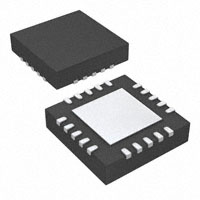
Device Information(1)
PART NUMBER
TPA2012D2
PACKAGE
BODY SIZE (NOM)
DSBGA (16)
2.01 mm × 2.01 mm
WQFN (20)
4.00 mm × 4.00 mm
(1) For all available packages, see the orderable addendum at
the end of the data sheet.
Simplified Application Schematic
Wireless or Cellular Handsets and PDAs
Portable DVD Players
Notebook PCs
Portable Radios
Portable Gaming
Educational Toys
USB Speakers
Copyright © 2016, Texas Instruments Incorporated
1
An IMPORTANT NOTICE at the end of this data sheet addresses availability, warranty, changes, use in safety-critical applications,
intellectual property matters and other important disclaimers. PRODUCTION DATA.
�TPA2012D2
SLOS438F – DECEMBER 2004 – REVISED MARCH 2017
www.ti.com
Table of Contents
1
2
3
4
5
6
7
8
9
Features ..................................................................
Applications ...........................................................
Description .............................................................
Revision History.....................................................
Device Comparison Table.....................................
Pin Configuration and Functions .........................
Specifications.........................................................
1
1
1
2
3
3
4
7.1
7.2
7.3
7.4
7.5
7.6
7.7
4
4
4
4
5
5
6
Absolute Maximum Ratings ......................................
ESD Ratings..............................................................
Recommended Operating Conditions.......................
Thermal Information ..................................................
Electrical Characteristics...........................................
Dissipation Rating Table ...........................................
Typical Characteristics ..............................................
Parameter Measurement Information ................ 12
Detailed Description ............................................ 13
9.1 Overview ................................................................. 13
9.2 Functional Block Diagram ....................................... 13
9.3 Feature Description................................................. 13
9.4 Device Functional Modes........................................ 15
10 Application and Implementation........................ 16
10.1 Application Information.......................................... 16
10.2 Typical Applications .............................................. 16
11 Power Supply Recommendations ..................... 19
11.1 Power Supply Decoupling Capacitor .................... 19
12 Layout................................................................... 19
12.1 Layout Guidelines ................................................. 19
12.2 Layout Examples................................................... 21
12.3 Efficiency and Thermal Considerations ................ 23
13 Device and Documentation Support ................. 24
13.1
13.2
13.3
13.4
13.5
Receiving Notification of Documentation Updates
Community Resources..........................................
Trademarks ...........................................................
Electrostatic Discharge Caution ............................
Glossary ................................................................
24
24
24
24
24
14 Mechanical, Packaging, and Orderable
Information ........................................................... 24
4 Revision History
NOTE: Page numbers for previous revisions may differ from page numbers in the current version.
Changes from Revision E (September 2016) to Revision F
•
Page
Switched the BODY SIZE values in the Device Information table: DSBGA From: 4.00 mm × 4.00 mm To: 2.01 mm ×
2.01 mm and WQFN From: 2.01 mm × 2.01 mm To: 4.00 mm × 4.00 mm........................................................................... 1
Changes from Revision D (June 2008) to Revision E
Page
•
Added ESD Ratings table, Feature Description section, Device Functional Modes, Application and Implementation
section, Power Supply Recommendations section, Layout section, Device and Documentation Support section, and
Mechanical, Packaging, and Orderable Information section .................................................................................................. 1
•
Deleted Available-Options table; see POA at the end of the data sheet ............................................................................... 1
•
Deleted previous application schematics: Typical Application Circuit (previously Figure 33), TPA2012D2 Application
Schematic With Differential Input and Input Capacitors (previously Figure 34), and TPA2012D2 Application
Schematic With Single-Ended Input (previously Figure 35) ................................................................................................. 16
2
Submit Documentation Feedback
Copyright © 2004–2017, Texas Instruments Incorporated
Product Folder Links: TPA2012D2
�TPA2012D2
www.ti.com
SLOS438F – DECEMBER 2004 – REVISED MARCH 2017
5 Device Comparison Table
DEVICE NO.
SPEAKER AMP TYPE
SPECIAL FEATURE
OUTPUT POWER (M)
PSRR (dB)
TPA2012D2
Class D
—
2.1
71
TPA2016D2
Class D
AGC/DRC
2.8
80
TPA2026D2
Class D
AGC/DRC
3.2
80
6 Pin Configuration and Functions
YZH Package
16-Pin DSBGA
Top View
INL±
G1
SDR
SDL
A
INL+
PVDD
OUTL+
OUTL±
2
PVDD
3
PGND
OUTL±
AGND
INR±
INR+
18
17
16
14
OUTR+
13
PVDD
4
12
PGND
5
11
OUTR±
Thermal Pad
10
B
OUTL+
NC
PGND
G0
9
AGND
15
AVDD
G0
1
8
INR±
G1
SDR
OUTR±
INL±
OUTR+
19
AVDD
7
INR+
SDL
4
INL+
3
20
2
6
C
1
NC
D
RTJ Package
20-Pin WQFN
Top View
Not to scale
Not to scale
Pin Functions
PIN
I/O
DESCRIPTION
NAME
DSBGA
WQFN
AGND
C3
18
I
Analog ground
AVDD
D2
9
I
Analog supply (must be same voltage as PVDD)
G0
C2
15
I
Gain select (LSB)
G1
B2
1
I
Gain select (MSB)
INL–
B1
19
I
Left channel negative input
INL+
A1
20
I
Left channel positive input
INR–
C1
17
I
Right channel negative input
INR+
D1
16
I
Right channel positive input
NC
—
6, 10
—
No internal connection
OUTL–
A4
5
O
Left channel negative differential output
OUTL+
A3
2
O
Left channel positive differential output
OUTR–
D4
11
O
Right channel negative differential output
OUTR+
D3
14
O
Right channel positive differential output
PGND
C4
4, 12
I
Power ground
PVDD
A2
3, 13
I
Power supply (must be same voltage as AVDD)
SDL
B4
7
I
Left channel shutdown terminal (active low)
SDR
B3
8
I
Right channel shutdown terminal (active low)
Thermal Pad
—
—
—
Connect the thermal pad of WQFN package to PCB GND
Submit Documentation Feedback
Copyright © 2004–2017, Texas Instruments Incorporated
Product Folder Links: TPA2012D2
3
�TPA2012D2
SLOS438F – DECEMBER 2004 – REVISED MARCH 2017
www.ti.com
7 Specifications
7.1 Absolute Maximum Ratings
over operating free-air temperature range (unless otherwise noted) (1)
Supply voltage, VSS (AVDD, PVDD)
MIN
MAX
Active mode
–0.3
6
Shutdown mode
–0.3
7
–0.3
VDD + 0.3
Input voltage, VI
Continuous total power dissipation
UNIT
V
V
See Dissipation Rating Table
Operating junction temperature, TJ
–40
150
°C
Storage temperature, Tstg
–65
150
°C
(1)
Stresses beyond those listed under Absolute Maximum Ratings may cause permanent damage to the device. These are stress ratings
only, which do not imply functional operation of the device at these or any other conditions beyond those indicated under Recommended
Operating Conditions. Exposure to absolute-maximum-rated conditions for extended periods may affect device reliability.
7.2 ESD Ratings
VALUE
V(ESD)
(1)
(2)
Electrostatic discharge
Human-body model (HBM), per ANSI/ESDA/JEDEC JS-001 (1)
±2000
Charged-device model (CDM), per JEDEC specification JESD22-C101 (2)
±1500
UNIT
V
JEDEC document JEP155 states that 500-V HBM allows safe manufacturing with a standard ESD control process.
JEDEC document JEP157 states that 250-V CDM allows safe manufacturing with a standard ESD control process.
7.3 Recommended Operating Conditions
over operating free-air temperature range (unless otherwise noted)
MIN
MAX
5.5
VSS
Supply voltage, AVDD, PVDD
2.5
VIH
High-level input voltage, SDL, SDR, G0, G1
1.3
VIL
Low-level input voltage, SDL, SDR, G0, G1
TA
Operating free-air temperature
UNIT
V
V
0.35
V
85
°C
–40
7.4 Thermal Information
TPA2012D2
THERMAL METRIC
(1)
YZH (DSBGA)
RTJ (WQFN)
16 PINS
20 PINS
UNIT
RθJA
Junction-to-ambient thermal resistance
71.4
34.6
°C/W
RθJC(top)
Junction-to-case (top) thermal resistance
0.4
34.3
°C/W
RθJB
Junction-to-board thermal resistance
14
11.5
°C/W
ψJT
Junction-to-top characterization parameter
1.8
0.4
°C/W
ψJB
Junction-to-board characterization parameter
13.3
11.6
°C/W
RθJC(bot)
Junction-to-case (bottom) thermal resistance
—
3.2
°C/W
(1)
4
For more information about traditional and new thermal metrics, see the Semiconductor and IC Package Thermal Metrics application
report.
Submit Documentation Feedback
Copyright © 2004–2017, Texas Instruments Incorporated
Product Folder Links: TPA2012D2
�TPA2012D2
www.ti.com
SLOS438F – DECEMBER 2004 – REVISED MARCH 2017
7.5 Electrical Characteristics
TA = 25°C (unless otherwise noted)
PARAMETER
TEST CONDITIONS
MIN
|VOO|
Output offset voltage (measured
differentially)
Inputs ac grounded, AV = 6 dB, VDD = 2.5 to 5.5 V
PSRR
Power supply rejection ratio
VDD = 2.5 to 5.5 V
Vicm
Common-mode input voltage
CMRR
Common-mode rejection ration
Inputs shorted together, VDD = 2.5 to 5.5 V
|IIH|
High-level input current
|IIL|
Low-level input current
IDD
TYP
MAX
5
25
mV
–55
dB
–75
0.5
Supply current
VDD – 0.8
V
–50
dB
VDD = 5.5 V, VI = VDD
50
µA
VDD = 5.5 V, VI = 0 V
5
µA
–69
VDD = 5.5 V, no load or output filter
6
9
VDD = 3.6 V, no load or output filter
5
7.5
VDD = 2.5 V, no load or output filter
4
6
Shutdown mode
rDS(on)
f(sw)
Static drain-source on-state resistance
1.5
VDD = 5.5 V
500
VDD = 3.6 V
570
VDD = 2.5 V
700
Output impedance in shutdown mode
V(SDR, SDL)= 0.35 V
Switching frequency
VDD = 2.5 V to 5.5 V
300
mA
µA
mΩ
2
250
G0, G1 = 0.35 V
Closed-loop voltage gain
UNIT
kΩ
350
5.5
6
6.5
G0 = VDD, G1 = 0.35 V
11.5
12
12.5
G0 = 0.35 V, G1 = VDD
17.5
18
18.5
G0, G1 = VDD
23.5
24
24.5
kHz
dB
OPERATING CHARACTERISTICS, RL = 8 Ω
VDD = 5 V, f = 1 kHz,
THD = 10%
RL = 8 Ω
PO
VDD = 3.6 V, f = 1 kHz,
THD = 10%
Output power (per channel)
Total harmonic distortion plus noise
Channel crosstalk
kSVR
Supply ripple rejection ratio
CMRR
Common mode rejection ratio
Input impedance
Vn
0.72
VDD = 5 V, f = 1 kHz,
THD = 10%
RL = 4 Ω
THD+N
1.4
2.1
PO = 1 W, VDD = 5 V, AV = 6 dB, f = 1 kHz
0.14%
PO = 0.5 W, VDD = 5 V, AV = 6 dB, f = 1 kHz
0.11%
f = 1 kHz
–85
VDD = 5 V, AV = 6 dB, f = 217 Hz
–77
VDD = 3.6 V, AV = 6 dB, f = 217 Hz
–73
VDD = 3.6 V, VIC = 1 Vpp, f = 217 Hz
–69
Av = 6 dB
28.1
Av = 12 dB
17.3
Av = 18 dB
9.8
Av = 24 dB
5.2
Start-up time from shutdown
VDD = 3.6 V
Output voltage noise
VDD = 3.6 V, f = 20 to 20 kHz,
inputs are ac grounded,
AV = 6 dB
W
dB
dB
dB
kΩ
3.5
No weighting
35
A weighting
27
ms
µV
7.6 Dissipation Rating Table
(1)
PACKAGE
TA = 25°C
POWER RATING (1)
DERATING
FACTOR
TA = 75°C
POWER RATING
TA = 85°C
POWER RATING
RTJ
5.2 W
41.6 mW/°C
3.12 W
2.7 W
YZH
1.2 W
9.12 mW/°C
690 mW
600 mW
This data was taken using 2-oz trace and copper pad that is soldered directly to a JEDEC standard 4-layer 3 in × 3 in PCB.
Submit Documentation Feedback
Copyright © 2004–2017, Texas Instruments Incorporated
Product Folder Links: TPA2012D2
5
�TPA2012D2
SLOS438F – DECEMBER 2004 – REVISED MARCH 2017
www.ti.com
7.7 Typical Characteristics
20
RL = 8 W,
f = 1 kHz,
AV 24 dB
THD+N − Total Harmonic Distortion + Noise − %
THD+N − Total Harmonic Distortion + Noise − %
20
10
2.5 V
1
3.6 V
0.1
5V
0.01
0.01
0.1
PO − Output Power − W
1
10
2.5 V
1
3.6 V
0.1
5V
0.01
0.01
3
20
RL = 4 W,
f = 1 kHz,
AV = 24 dB
2.5 V
1
3.6 V
0.1
5V
0.01
0.01
0.1
1
0.1
PO − Output Power − W
10
RL = 4 W,
f = 1 kHz,
AV = 6 dB
2.5 V
1
3.6 V
0.1
5V
0.01
0.01
4
0.1
4
Figure 4. Total Harmonic Distortion
vs Output Power
1
VDD = 2.5 V,
RL = 4 W,
CI = 1 mF,
AV = 6 dB
120 mW
350 mW
0.1
240 mW
100
1k
f − Frequency − Hz
10 k 20 k
Figure 5. Total Harmonic Distortion vs Frequency
THD+N − Total Harmonic Distortion + Noise − %
1
THD+N − Total Harmonic Distortion + Noise − %
1
PO − Output Power − W
Figure 3. Total Harmonic Distortion
vs Output Power
6
3
20
PO − Output Power − W
0.01
20
1
Figure 2. Total Harmonic Distortion
vs Output Power
THD+N − Total Harmonic Distortion + Noise − %
THD+N − Total Harmonic Distortion + Noise − %
Figure 1. Total Harmonic Distortion
vs Output Power
10
RL = 8 W,
f = 1 kHz,
AV 6 dB
VDD = 2.5 V,
RL = 8 W,
CI = 1 mF,
AV = 6 dB
90 mW
260 mW
0.1
180 mW
0.01
20
100
1k
f − Frequency − Hz
10 k 20 k
Figure 6. Total Harmonic Distortion vs Frequency
Submit Documentation Feedback
Copyright © 2004–2017, Texas Instruments Incorporated
Product Folder Links: TPA2012D2
�TPA2012D2
www.ti.com
SLOS438F – DECEMBER 2004 – REVISED MARCH 2017
Typical Characteristics (continued)
1
VDD = 3.6 V,
RL = 4 W,
CI = 1 mF,
AV = 6 dB
THD+N − Total Harmonic Distortion + Noise − %
THD+N − Total Harmonic Distortion + Noise − %
1
275 mW
825 mW
0.1
550 mW
0.01
20
100
1k
f − Frequency − Hz
0.1
375 mW
100
1k
f − Frequency − Hz
10 k 20 k
Figure 8. Total Harmonic Distortion vs Frequency
1
VDD = 5 V,
RL = 4 W,
CI = 1 mF,
AV = 6 dB
THD+N − Total Harmonic Distortion + Noise − %
1
THD+N − Total Harmonic Distortion + Noise − %
190 mW
560 mW
0.01
20
10 k 20 k
Figure 7. Total Harmonic Distortion vs Frequency
VDD = 3.6 V,
RL = 8 W,
CI = 1 mF,
AV = 6 dB
550 mW
0.1
1.65 W
1.1 W
0.01
20
100
1k
f − Frequency − Hz
10 k 20 k
Figure 9. Total Harmonic Distortion vs Frequency
VDD = 5 V,
RL = 8 W,
CI = 1 mF,
AV = 6 dB
380 mW
1.16 W
0.1
775 mW
0.01
20
100
1k
f − Frequency − Hz
10 k
20 k
Figure 10. Total Harmonic Distortion vs Frequency
6
I DD − Supply Current − mA
VDD = 5 V
5
VDD = 3.6 V
4
VDD = 2.5 V
3
2
1
No Output Filter
0
0
1
2
3
4
VSD − Shutdown Voltage − V
5
Figure 11. Supply Current vs Shutdown Voltage
Figure 12. Supply Current vs Supply Voltage
Submit Documentation Feedback
Copyright © 2004–2017, Texas Instruments Incorporated
Product Folder Links: TPA2012D2
7
�TPA2012D2
SLOS438F – DECEMBER 2004 – REVISED MARCH 2017
www.ti.com
Typical Characteristics (continued)
800
1200
IDD is for Both Channels
IDD is for Both Channels
700
I DD − Supply Current − mA
I DD − Supply Current − mA
1000
600
500
400
300
VDD = 5 V, RL = 8 W, 33 mH
200
VDD = 3.6 V, RL = 8 W, 33 mH
0
0
0.2
0.4
0.6
0.8
1
600
VDD = 5 V, RL = 4 W, 33 mH
400
VDD = 3.6 V, RL = 4 W, 33 mH
200
VDD = 2.5 V, RL = 8 W, 33 mH
100
800
VDD = 2.5 V, RL = 4 W, 33 mH
1.2
1.4
0
1.6
0
0.2 0.4 0.6 0.8 1 1.2 1.4 1.6 1.8
PO − Output Power/Channel − W
PO − Output Power/Channel − W
Figure 13. Supply Current vs Output Power
2
2.2
Figure 14. Supply Current vs Output Power
0
0
RI = 8
−20
RI = 4
−20
Crosstalk − dB
Crosstalk − dB
−40
−60
2.5 V R to L
−80
2.5 V L to R
5 V R to L
−40
−60
2.5 V R to L
−80
−100
−120
−140
20
100
5 V L to R
5 V L to R
1k
f − Frequency − Hz
−120
10 k 20 k
20
100
Inputs AC, Grounded,
CI = 1 mF,
RI = 4 W
AV = 6 dB
−50
VDD = 2.7 V
−60
−70
−80
VDD = 3.6 V
−90
−100
20
VDD = 5 V
1k
f − Frequency − Hz
10 k
10 k 20 k
Inputs AC Grounded,
CI = 1 mF,
RI = 8 W,
AV = 6 dB
−50
VDD = 2.7 V
−60
−70
−80
VDD = 3.6 V
−90
20 k
VDD = 5 V
20
100
1k
10 k 20 k
f − Frequency − Hz
Figure 17. Power Supply Rejection Ratio
vs Frequency
8
−40
−100
100
1k
f − Frequency − Hz
Figure 16. Crosstalk vs Frequency
−30
PSRR − Power Supply Rejection Ratio − dB
PSRR − Power Supply Rejection Ratio − dB
−40
5 V R to L
3.6 V R to L
Figure 15. Crosstalk vs Frequency
−30
3.6 V L to R
−100
3.6 V L to R
3.6 V R to L
2.5 V L to R
Figure 18. Power Supply Rejection Ratio
vs Frequency
Submit Documentation Feedback
Copyright © 2004–2017, Texas Instruments Incorporated
Product Folder Links: TPA2012D2
�TPA2012D2
www.ti.com
SLOS438F – DECEMBER 2004 – REVISED MARCH 2017
20
−50
VDD = 3.6 V
0
VIC = 1 VPP,
RL = 8 W,
AV = 6 dB
−20
VDD = 5.5 V
−40
−60
−80
−55
−60
−65
VDD = 3.6 V
−70
VDD = 5 V
−100
0
−75
1
2
3
4
5
VICR − Common-Mode Input Voltage Range − V
100
20
Figure 19. Common-Mode Rejection Ratio
vs Common-Mode Input Voltage
1k
f − Frequency − Hz
0
CI = 1 mF,
Inputs AC Grounded,
AV = 6 dB
VDD = 3.6 V
Input
Supply Signal Ripple − V
−20
VOUT
20 mV/div
10 k 20 k
Figure 20. Common-Mode Rejection Ratio
vs Frequency
C1 − High, 3.6 V
C1 − Amp, 512 mV
C1 − Duty, 12%
VDD
200 mV/div
VDD = 2.5 V
−40
−60
−60
−80
−80
−100
−100
−120
−120
−140
Output
−160
0
500
1000
2000
−160
2500
Figure 22. Power Supply Rejection vs Frequency
0.7
0
RL = 4 W
RL = 8 ,
VIN = 200 mVPP
f = 217 Hz
Class-AB,
VDD = 3.6 V
0.6
PD − Power Dissipation − W
k SVR − Supply Voltage Rejection Ratio − dB
1500
f − Frequency − Hz
t − Time − 2 ms/div
Figure 21. GSM Power Supply Rejection vs Time
−20
VDD = 3.6 V
−30
VDD = 5 V
−40
VDD = 2.7 V
−50
−60
−70
0.5
Class-AB,
VDD = 3.6 V
0.4
RL = 8 W
QFN
0.2
0.1
RL = 8 W
Powers are per Channel
0
0.5
1
1.5
2
2.5
3
3.5
4
4.5
RL = 4 W
0.3
−80
−90
0
−20
−40
−140
−10
0
Power-Supply Rejection Output − V
VDD = 2.5 V
CMRR − Common-Mode Rejection Ratio − dB
CMRR − Common-Mode Rejection Ratio − dB
Typical Characteristics (continued)
0
5
0.2
0.4
0.6
0.8
1
1.2
1.4
PO − Output Power − W
DC Common Mode Voltage − V
Figure 23. Supply Voltage Rejection Ratio
vs DC Common-Mode Voltage
Figure 24. Power Dissipation vs Output Power
Submit Documentation Feedback
Copyright © 2004–2017, Texas Instruments Incorporated
Product Folder Links: TPA2012D2
9
�TPA2012D2
SLOS438F – DECEMBER 2004 – REVISED MARCH 2017
www.ti.com
Typical Characteristics (continued)
1.4
100
RL = 4 W
Class-AB, VDD = 5 V
80
1
Class-AB, VDD = 5 V
RL = 8 W
0.8
RL = 4 W
0.6
VDD = 3.6 V
60
VDD = 2.5 V
50
40
Class-AB
30
QFN
0.4
VDD = 5 V
70
Efficiency − %
PD − Power Dissipation − W
RL = 4 W
90
1.2
QFN
20
0.2
RL = 8 W
10
Powers are per Channel
Powers are per Channel
0
0
0.5
1
1.5
2
0
2.5
0
0.5
PO − Output Power − W
Figure 25. Power Dissipation vs Output Power
2.5
RL = 4 W
VDD = 5 V
0.6
PD − Power Dissipation − W
80
VDD = 3.6 V
70
VDD = 2.5 V
60
50
Class-AB
40
30
QFN
20
Class-AB, VDD = 3.6 V
0.5
Class-AB,
VDD = 3.6 V
RL = 8 W
0.4
RL = 4 W
0.3
0.2
WCSP
RL = 8 W
0.1
10
Powers are per Channel
Powers are per Channel
0
0
0
0.2
0.4
0.6
0.8
1
1.2
1.4
0
0.2
0.4
0.6
0.8
1
1.2
1.4
PO − Output Power − W
PO − Output Power − W
Figure 27. Efficiency vs Output Power
Figure 28. Power Dissipation vs Output Power
1.4
100
Class-AB, VDD = 5 V
1.2
RL = 4 W
90
RL = 4 W
80
1
VDD = 3.6 V
Efficiency − %
70
Class-AB, VDD = 5 V
RL = 8 W
0.8
WCSP
0.6
0.4
VDD = 5 V
60
50
40
Class-AB, VDD = 5 V
30
RL = 4 W
20
RL = 8 W
0.2
WCSP
10
Powers are per Channel
0
0
0
10
2
Figure 26. Efficiency vs Output Power
RL = 8 W
90
Efficiency − %
1.5
0.7
100
PD − Power Dissipation − W
1
PO − Output Power − W
0.5
1
1.5
2
2.5
0
0.2
0.4
0.6
0.8
1
1.2
1.4
1.6
PO − Output Power − W
PO − Output Power − W
Figure 29. Power Dissipation vs Output Power
Figure 30. Efficiency vs Output Power
Submit Documentation Feedback
Copyright © 2004–2017, Texas Instruments Incorporated
Product Folder Links: TPA2012D2
�TPA2012D2
www.ti.com
SLOS438F – DECEMBER 2004 – REVISED MARCH 2017
Typical Characteristics (continued)
2
100
RL = 8 W
VDD = 5 V
90
1.6
VDD = 3.6 V
70
PO − Output Power − W
Efficiency − %
80
60
50
40
Class-AB, VDD = 5 V
30
RL = 4 W
THD+N = 1%
1.4
RL = 8 W
THD+N = 10%
1.2
1
0.8
0.6
WCSP
20
0.4
10
0
RL = 4 W
THD+N = 10%
1.8
RL = 8 W
THD+N = 1%
0.2
0
0.2
0.4
0.6
0.8
1
1.2
0
2.5
1.4
3
PO − Output Power − W
3.5
4
4.5
VDD − Supply Voltage − V
5
Figure 32. Output Power vs Supply Voltage
Figure 31. Efficiency vs Output Power
2.50
PO − Output Power − W
WCSP Thermally Limited Region
VDD = 2.5 V, 1%
2
VDD = 2.5 V, 10%
VDD = 3.6 V, 1%
1.50
VDD = 3.6 V, 10%
VDD = 5 V, 1%
VDD = 3.6 V, 10%
1
0.50
0
4
9
14
19
24
29
34
RL − Load Resistance − W
Figure 33. Output Power vs Load Resistance
Submit Documentation Feedback
Copyright © 2004–2017, Texas Instruments Incorporated
Product Folder Links: TPA2012D2
11
�TPA2012D2
SLOS438F – DECEMBER 2004 – REVISED MARCH 2017
www.ti.com
8 Parameter Measurement Information
All parameters are measured according to the conditions described in the Specifications. Figure 34 shows the
setup used for the typical characteristics of the test device.
CI
TPA2012D2
RI
IN+
+
Measurement
Output
OUT+
+
Load
CI
RI
-
INVDD
+
OUT-
30 kHz
Low Pass
Filter
Measurement
Input
-
GND
1 µF
VDD
-
Copyright © 2016, Texas Instruments Incorporated
(1)
CI was shorted for any common-mode input voltage measurement.
(2)
A 33-µH inductor was placed in series with the load resistor to emulate a small speaker for efficiency measurements.
(3)
The 30-kHz low-pass filter is required even if the analyzer has an internal low-pass filter. An RC low-pass filter
(100 Ω, 47 nF) is used on each output for the data sheet graphs.
Figure 34. Test Setup For Graphs (Per Channel)
12
Submit Documentation Feedback
Copyright © 2004–2017, Texas Instruments Incorporated
Product Folder Links: TPA2012D2
�TPA2012D2
www.ti.com
SLOS438F – DECEMBER 2004 – REVISED MARCH 2017
9 Detailed Description
9.1 Overview
The TPA2012D2 is capable of driving 1.4 W/Ch at 5-V or 720 mW/Ch at 3.6-V into 8 Ω. The TPA2012D2 is also
capable of driving a load of 4 Ω.
The TPA2012D2 feature independent shutdown controls for each channel. High PSRR and differential
architecture provide increased immunity to noise and RF rectification. The TPA2012D2 provides thermal and
short-circuit protection.
9.2 Functional Block Diagram
V DD
to Battery
CS
INR+
OUTR+
Gain
Adjust
Right Input
PWM
Hí
Bridge
OUTRí
INRí
Internal
Oscillator
GND
OUTL+
INL+
Gain
Adjust
Left Input
PWM
Hí
Bridge
OUTLí
INLí
G0
G1
SDR
300 kŸ
Bias
Circuitry
ShortíCircuit
Protection
SDL
300 kŸ
Copyright © 2016, Texas Instruments Incorporated
9.3 Feature Description
9.3.1 Fixed Gain Setting
The TPA2012D2 has 4 selectable fixed gains: 6 dB, 12 dB, 18 dB, and 24 dB. Connect the G0 and G1 pins as
shown in Table 1.
Submit Documentation Feedback
Copyright © 2004–2017, Texas Instruments Incorporated
Product Folder Links: TPA2012D2
13
�TPA2012D2
SLOS438F – DECEMBER 2004 – REVISED MARCH 2017
www.ti.com
Table 1. Gain Setting
G1
G0
GAIN
(V/V)
GAIN
(dB)
INPUT IMPEDANCE
(RI, kΩ)
0
0
2
6
28.1
0
1
4
12
17.3
1
0
8
18
9.8
1
1
16
24
5.2
9.3.2 Short-Circuit Protection
TPA2012D2 goes to low duty cycle mode when a short-circuit event happens. To return to normal duty cycle
mode, the device must be reset. The shutdown mode can be set through the SDL and SDR pins, or the device
can be turned off and turned on to return to normal duty cycle mode. This feature protects the device without
affecting long-term reliability.
9.3.3 Operation With DACs and CODECs
In using Class-D amplifiers with CODECs and DACs, sometimes there is an increase in the output noise floor
from the audio amplifier. This occurs when mixing of the output frequencies of the CODEC and DAC mix with the
switching frequencies of the audio amplifier input stage. The noise increase can be solved by placing a low-pass
filter between the CODEC, DAC, and audio amplifier. This filters off the high frequencies that cause the problem
and allow proper performance. The recommended resistor value is 100 Ω and the capacitor value of 47 nF.
Figure 35 shows the typical input filter.
CI
INLINL+
CI
DAC or CODEC
TPA2012D2
CI
INRINR+
CI
Copyright © 2016, Texas Instruments Incorporated
Figure 35. Reducing Out-of-Band DAC Noise With External Input Filter
9.3.4 Filter-Free Operation and Ferrite Bead Filters
A ferrite bead filter can often be used if the design is failing radiated emissions without an LC filter and the
frequency sensitive circuit is greater than 1 MHz. This filter functions well for circuits that just have to pass FCC
and CE because FCC and CE only test radiated emissions greater than 30 MHz. When choosing a ferrite bead,
choose one with high impedance at high frequencies, and very low impedance at low frequencies. In addition,
select a ferrite bead with adequate current rating to prevent distortion of the output signal.
Use an LC output filter if there are low frequency (< 1 MHz) EMI sensitive circuits and/or there are long leads
from amplifier to speaker.
Figure 36 shows typical ferrite bead and LC output filters.
14
Submit Documentation Feedback
Copyright © 2004–2017, Texas Instruments Incorporated
Product Folder Links: TPA2012D2
�TPA2012D2
www.ti.com
SLOS438F – DECEMBER 2004 – REVISED MARCH 2017
Ferrite
Chip Bead
OUTP
1 nF
Ferrite
Chip Bead
OUTN
1 nF
Figure 36. Typical Ferrite Chip Bead Filter (Chip Bead Example: TDK – MPZ1608S221A)
9.4 Device Functional Modes
9.4.1 Shutdown Mode
The TPA2012D2 amplifier can be put in shutdown mode when asserting SDR and SDL pins to a logic LOW.
While in shutdown mode, the device output stage is turned off and the current consumption is very low.
Submit Documentation Feedback
Copyright © 2004–2017, Texas Instruments Incorporated
Product Folder Links: TPA2012D2
15
�TPA2012D2
SLOS438F – DECEMBER 2004 – REVISED MARCH 2017
www.ti.com
10 Application and Implementation
NOTE
Information in the following applications sections is not part of the TI component
specification, and TI does not warrant its accuracy or completeness. TI’s customers are
responsible for determining suitability of components for their purposes. Customers should
validate and test their design implementation to confirm system functionality.
10.1 Application Information
These typical connection diagrams highlight the required external components and system level connections for
proper operation of the device. Each of these configurations can be realized using the evaluation modules
(EVMs) for the device. These flexible modules allow full evaluation of the device in the most common modes of
operation. Any design variation can be supported by TI through schematic and layout reviews. Visit e2e.ti.com for
design assistance and join the audio amplifier discussion forum for additional information.
10.2 Typical Applications
10.2.1 TPA2012D2 With Differential Input Signal
To power supply
0.1 µF
10 µF
CI
PVdd
AVdd
TPA2012D2
INLOUTL+
CI
1 µF
INL+
DAC or CODEC
CI
CI
OUTLINR-
G0
G1
INR+
OUTR+
1 µF
1 µF
Shutdown
Control
SDL
SDR
AGND
OUTRPGND
1 µF
Copyright © 2016, Texas Instruments Incorporated
Figure 37. Typical Application Schematic With Differential Input Signals
16
Submit Documentation Feedback
Copyright © 2004–2017, Texas Instruments Incorporated
Product Folder Links: TPA2012D2
�TPA2012D2
www.ti.com
SLOS438F – DECEMBER 2004 – REVISED MARCH 2017
Typical Applications (continued)
10.2.1.1 Design Requirements
For this design example, use the parameters listed in Table 2.
Table 2. Design Parameters
PARAMETER
VALUE
Power supply
Enable inputs
Speaker
5V
High > 1.3 V
Low < 0.35 V
8Ω
10.2.1.2 Detailed Design Procedure
10.2.1.2.1 Surface Mount Capacitors
Temperature and applied DC voltage influence the actual capacitance of high-K materials. Table 3 shows the
relationship between the different types of high-K materials and their associated tolerances, temperature
coefficients, and temperature ranges. Notice that a capacitor made with X5R material can lose up to 15% of its
capacitance within its working temperature range.
In an application, the working capacitance of components made with high-K materials is generally much lower
than nominal capacitance. A worst-case result with a typical X5R material might be –10% tolerance, –15%
temperature effect, and –45% DC voltage effect at 50% of the rated voltage. This particular case would result in
a working capacitance of 42% (0.9 × 0.85 × 0.55) of the nominal value.
Select high-K ceramic capacitors according to the following rules:
1. Use capacitors made of materials with temperature coefficients of X5R, X7R, or better.
2. Use capacitors with DC voltage ratings of at least twice the application voltage. Use minimum 10-V
capacitors for the TPA2012D2.
3. Choose a capacitance value at least twice the nominal value calculated for the application. Multiply the
nominal value by a factor of 2 for safety. If a 10-µF capacitor is required, use 20 µF.
The preceding rules and recommendations apply to capacitors used in connection with the TPA2012D2. The
TPA2012D2 cannot meet its performance specifications if the rules and recommendations are not followed.
Table 3. Typical Tolerance and Temperature Coefficient of Capacitance by Material
MATERIAL
COG/NPO
X7R
X5R
Typical tolerance
±5%
±10%
80% to –20%
Temperature
±30 ppm
±15%
22% to –82%
Temperature range (°C)
–55°C to 125°C
–55°C to 125°C
–30°C to 85°C
10.2.1.2.2 Decoupling Capacitor (CS)
The TPA2012D2 is a high-performance Class-D audio amplifier that requires adequate power supply decoupling
to ensure the efficiency is high and total harmonic distortion (THD) is low. For higher frequency transients,
spikes, or digital hash on the line a good low equivalent-series-resistance (ESR) ceramic capacitor, typically
1 µF, placed as close as possible to the device PVDD lead works best. Placing this decoupling capacitor close to
the TPA2012D2 is important for the efficiency of the Class-D amplifier, because any resistance or inductance in
the trace between the device and the capacitor can cause a loss in efficiency. For filtering lower-frequency noise
signals, a 4.7 µF or greater capacitor placed near the audio power amplifier would also help, but it is not required
in most applications because of the high PSRR of this device.
10.2.1.2.3 Input Capacitors (CI)
The TPA2012D2 does not require input coupling capacitors if the design uses a differential source that is biased
from 0.5 V to VDD – 0.8 V. If the input signal is not biased within the recommended common-mode input range, if
high-pass filtering is needed (see Figure 37), or if using a single-ended source (see Figure 38), input coupling
capacitors are required.
Submit Documentation Feedback
Copyright © 2004–2017, Texas Instruments Incorporated
Product Folder Links: TPA2012D2
17
�TPA2012D2
SLOS438F – DECEMBER 2004 – REVISED MARCH 2017
www.ti.com
The input capacitors and input resistors form a high-pass filter with the corner frequency, fc, determined in
Equation 1.
1
fC =
(2p RI CI )
(1)
The value of the input capacitor is important to consider as it directly affects the bass (low frequency)
performance of the circuit. Speakers in wireless phones cannot usually respond well to low frequencies, so the
corner frequency can be set to block low frequencies in this application. Not using input capacitors can increase
output offset.
Equation 2 is used to solve for the input coupling capacitance.
1
CI =
(2p RI fC )
(2)
If the corner frequency is within the audio band, the capacitors should have a tolerance of ±10% or better,
because any mismatch in capacitance causes an impedance mismatch at the corner frequency and below.
10.2.1.3 Application Curves
For application curves, see the figures listed in Table 4.
Table 4. Table of Graphs
(1)
DESCRIPTION
FIGURE NO. (1)
THD+N vs Output power
Figure 1
THD+N vs Frequency
Figure 5
Power dissipation vs Output power
Figure 24
Output power vs Supply voltage
Figure 32
All figure numbers have a hyperlink to a figure in the Typical Characteristics.
10.2.2 TPA2012D2 With Single-Ended Input Signal
To power supply
0.1 µF
10 µF
PVdd
AVdd
TPA2012D2
INLOUTL+
INL+
CI
1 µF
CI
DAC or CODEC
OUTLCI
INRINR+
CI
G0
G1
1 µF
OUTR+
1 µF
Shutdown
Control
SDL
SDR
AGND
OUTRPGND
1 µF
Copyright © 2016, Texas Instruments Incorporated
Figure 38. Typical Application Schematic With Single-Ended Input Signal
18
Submit Documentation Feedback
Copyright © 2004–2017, Texas Instruments Incorporated
Product Folder Links: TPA2012D2
�TPA2012D2
www.ti.com
SLOS438F – DECEMBER 2004 – REVISED MARCH 2017
10.2.2.1 Design Requirements
For this design example, use the parameters listed in Table 2.
10.2.2.2 Detailed Design Procedure
For the design procedure, see Detailed Design Procedure from the previous example.
10.2.2.3 Application Curves
For application curves, see the figures listed in Table 4.
11 Power Supply Recommendations
The TPA2012D2 is designed to operate from an input voltage supply range from 2.5 V to 5.5 V. Therefore, the
output voltage range of the power supply must be within this range. The current capability of upper power must
not exceed the maximum current limit of the power switch.
11.1 Power Supply Decoupling Capacitor
The TPA2012D2 requires adequate power supply decoupling to ensure a high efficiency operation with low total
harmonic distortion (THD). Place a low equivalent-series-resistance (ESR) ceramic capacitor, typically 0.1-µF,
within 2 mm of the PVDD/AVDD pins. This choice of capacitor and placement helps with higher frequency
transients, spikes, or digital hash on the line. In addition to the 0.1-µF ceramic capacitor, TI recommends placing
a 2.2-µF to 10-µF capacitor on the PVDD/AVDD supply trace. This larger capacitor acts as a charge reservoir,
providing energy faster than the board supply, thus helping to prevent any droop in the supply voltage.
12 Layout
12.1 Layout Guidelines
12.1.1 Pad Side
In making the pad size for the DSBGA balls, TI recommends that the layout use non-solder mask defined
(NSMD) land. With this method, the solder mask opening is made larger than the desired land area, and the
opening size is defined by the copper pad width. Figure 39 and Table 5 shows the appropriate diameters for a
DSBGA layout. The TPA2012D2 evaluation module (EVM) layout is shown in the next section as a layout
example.
Table 5. Land Pattern Dimensions (1) (2) (3) (4)
SOLDER PAD
DEFINITIONS
COPPER
PAD
SOLDER MASK (5)
OPENING
COPPER
THICKNESS
STENCIL (6) (7)
OPENING
STENCIL
THICKNESS
Nonsolder mask
defined (NSMD)
275 µm
(+0.0, –25 µm)
375 µm (+0.0, –25 µm)
1 oz max (32 µm)
275 µm × 275 µm
(square)
(rounded corners)
125 µm
(1)
(2)
(3)
(4)
(5)
(6)
(7)
Circuit traces from NSMD defined PWB lands should be 75 µm to 100 µm wide in the exposed area inside the solder mask opening.
Wider trace widths reduce device stand off and impact reliability.
Best reliability results are achieved when the PWB laminate glass transition temperature is above the operating the range of the
intended application.
Recommend solder paste is Type 3 or Type 4.
For a PWB using a Ni/Au surface finish, the gold thickness should be less 0.5 mm to avoid a reduction in thermal fatigue performance.
Solder mask thickness should be less than 20 µm on top of the copper circuit pattern
Best solder stencil performance is achieved using laser cut stencils with electro polishing. Use of chemically etched stencils results in
inferior solder paste volume control.
Trace routing away from DSBGA device should be balanced in X and Y directions to avoid unintentional component movement due to
solder wetting forces.
Submit Documentation Feedback
Copyright © 2004–2017, Texas Instruments Incorporated
Product Folder Links: TPA2012D2
19
�TPA2012D2
SLOS438F – DECEMBER 2004 – REVISED MARCH 2017
www.ti.com
Copper
Trace Width
Solder
Pad Width
Solder Mask
Opening
Copper Trace
Thickness
Solder Mask
Thickness
Figure 39. Land Pattern Dimensions
12.1.2 Component Location
Place all the external components very close to the TPA2012D2. Placing the decoupling capacitor, CS, close to
the TPA2012D2 is important for the efficiency of the Class-D amplifier. Any resistance or inductance in the trace
between the device and the capacitor can cause a loss in efficiency.
12.1.3 Trace Width
Recommended trace width at the solder balls is 75 µm to 100 µm to prevent solder wicking onto wider PCB
traces.
For high current pins (PVDD, PGND, and audio output pins) of the TPA2012D2, use 100-µm trace widths at the
solder balls and at least 500-µm PCB traces to ensure proper performance and output power for the device.
For the remaining signals of the TPA2012D2, use 75-µm to 100-µm trace widths at the solder balls. The audio
input pins (INR± and INL±) must run side-by-side to maximize common-mode noise cancellation.
20
Submit Documentation Feedback
Copyright © 2004–2017, Texas Instruments Incorporated
Product Folder Links: TPA2012D2
�TPA2012D2
www.ti.com
SLOS438F – DECEMBER 2004 – REVISED MARCH 2017
12.2 Layout Examples
Decoupling Capacitor
Placed As Close As
Possible to the Device
OUTL+ OUTL10µF
1µF
CI
G1
INL+
A1
A2
A3
A4
B1
B2
B3
B4
C1
C2
C3
C4
D1
D2
D3
D4
SDR
INLCI
SDL
INRG0
INR+
1µF TPA2012D2
CI
10µF
Input Capacitors
Placed As Close As
Possible to the Device
OUTR+ OUTR-
Top Layer Ground Plane
Top Layer Traces
Pad to Top Layer Ground Plane
Bottom Layer Traces
Via to Ground Plane
Via to Bottom Layer
Via to Power Supply Plane
Figure 40. TPA2012D2 DSBGA Layout Example
Submit Documentation Feedback
Copyright © 2004–2017, Texas Instruments Incorporated
Product Folder Links: TPA2012D2
21
�TPA2012D2
SLOS438F – DECEMBER 2004 – REVISED MARCH 2017
www.ti.com
Layout Examples (continued)
INL+ INL- INR- INR+
CI
CI
G1
20
OUTL+
1µF
10µF
19
18
Input Capacitors
Placed As Close As
Possible to the Device
CI
17
G0
16
1
15
2
14
3
13
4
12
5
11
OUTR+
10µF
1µF
6
7
8
9
10
TPA2012D2
OUTL-
Decoupling Capacitor
Placed As Close As
Possible to the Device
OUTR-
10µF
Decoupling Capacitor
Placed As Close As
Possible to the Device
1µF
SDL SDR
Top Layer Ground Plane
Top Layer Traces
Pad to Top Layer Ground Plane
Thermal Pad
Via to Bottom Ground Plane
Via to Power Supply Plane
Figure 41. TPA2012D2 WQFN Layout Example
22
Submit Documentation Feedback
Copyright © 2004–2017, Texas Instruments Incorporated
Product Folder Links: TPA2012D2
�TPA2012D2
www.ti.com
SLOS438F – DECEMBER 2004 – REVISED MARCH 2017
12.3 Efficiency and Thermal Considerations
The maximum ambient temperature depends on the heat-sinking ability of the PCB system. The derating factor
for the packages are shown in the dissipation rating table. Converting this to θJA for the WQFN package with
Equation 3.
1
1
qJA =
=
= 24°C / W
Derating Factor 0.041
(3)
Given θJA of 24°C/W, the maximum allowable junction temperature of 150°C, and the maximum internal
dissipation of 1.5 W (0.75 W per channel) for 2.1 W per channel, 4-Ω load, 5-V supply, from Figure 25, the
maximum ambient temperature can be calculated with Equation 4.
TAMax = TJMax - qJAPDmax = 150 - 24(1.5) = 114°C
(4)
Equation 4 shows that the calculated maximum ambient temperature is 114°C at maximum power dissipation
with a 5-V supply and a 4-Ω load. The TPA2012D2 is designed with thermal protection that turns the device off
when the junction temperature surpasses 150°C to prevent damage to the IC. Also, using speakers more
resistive than 4-Ω dramatically increases the thermal performance by reducing the output current and increasing
the efficiency of the amplifier.
Submit Documentation Feedback
Copyright © 2004–2017, Texas Instruments Incorporated
Product Folder Links: TPA2012D2
23
�TPA2012D2
SLOS438F – DECEMBER 2004 – REVISED MARCH 2017
www.ti.com
13 Device and Documentation Support
13.1 Receiving Notification of Documentation Updates
To receive notification of documentation updates, navigate to the device product folder on ti.com. In the upper
right corner, click on Alert me to register and receive a weekly digest of any product information that has
changed. For change details, review the revision history included in any revised document.
13.2 Community Resources
The following links connect to TI community resources. Linked contents are provided "AS IS" by the respective
contributors. They do not constitute TI specifications and do not necessarily reflect TI's views; see TI's Terms of
Use.
TI E2E™ Online Community TI's Engineer-to-Engineer (E2E) Community. Created to foster collaboration
among engineers. At e2e.ti.com, you can ask questions, share knowledge, explore ideas and help
solve problems with fellow engineers.
Design Support TI's Design Support Quickly find helpful E2E forums along with design support tools and
contact information for technical support.
13.3 Trademarks
NanoFree, PowerPAD, E2E are trademarks of Texas Instruments.
All other trademarks are the property of their respective owners.
13.4 Electrostatic Discharge Caution
These devices have limited built-in ESD protection. The leads should be shorted together or the device placed in conductive foam
during storage or handling to prevent electrostatic damage to the MOS gates.
13.5 Glossary
SLYZ022 — TI Glossary.
This glossary lists and explains terms, acronyms, and definitions.
14 Mechanical, Packaging, and Orderable Information
The following pages include mechanical, packaging, and orderable information. This information is the most
current data available for the designated devices. This data is subject to change without notice and revision of
this document. For browser-based versions of this data sheet, refer to the left-hand navigation.
24
Submit Documentation Feedback
Copyright © 2004–2017, Texas Instruments Incorporated
Product Folder Links: TPA2012D2
�PACKAGE OPTION ADDENDUM
www.ti.com
19-Oct-2022
PACKAGING INFORMATION
Orderable Device
Status
(1)
Package Type Package Pins Package
Drawing
Qty
Eco Plan
(2)
Lead finish/
Ball material
MSL Peak Temp
Op Temp (°C)
Device Marking
(3)
Samples
(4/5)
(6)
TPA2012D2RTJR
ACTIVE
QFN
RTJ
20
3000
RoHS & Green
NIPDAU
Level-2-260C-1 YEAR
-40 to 85
AKS
Samples
TPA2012D2RTJT
ACTIVE
QFN
RTJ
20
250
RoHS & Green
NIPDAU
Level-2-260C-1 YEAR
-40 to 85
AKS
Samples
TPA2012D2RTJTG4
ACTIVE
QFN
RTJ
20
250
RoHS & Green
NIPDAU
Level-2-260C-1 YEAR
-40 to 85
AKS
Samples
TPA2012D2YZHR
ACTIVE
DSBGA
YZH
16
3000
RoHS & Green
SNAGCU
Level-1-260C-UNLIM
-40 to 85
AKR
Samples
TPA2012D2YZHT
ACTIVE
DSBGA
YZH
16
250
RoHS & Green
SNAGCU
Level-1-260C-UNLIM
-40 to 85
AKR
Samples
(1)
The marketing status values are defined as follows:
ACTIVE: Product device recommended for new designs.
LIFEBUY: TI has announced that the device will be discontinued, and a lifetime-buy period is in effect.
NRND: Not recommended for new designs. Device is in production to support existing customers, but TI does not recommend using this part in a new design.
PREVIEW: Device has been announced but is not in production. Samples may or may not be available.
OBSOLETE: TI has discontinued the production of the device.
(2)
RoHS: TI defines "RoHS" to mean semiconductor products that are compliant with the current EU RoHS requirements for all 10 RoHS substances, including the requirement that RoHS substance
do not exceed 0.1% by weight in homogeneous materials. Where designed to be soldered at high temperatures, "RoHS" products are suitable for use in specified lead-free processes. TI may
reference these types of products as "Pb-Free".
RoHS Exempt: TI defines "RoHS Exempt" to mean products that contain lead but are compliant with EU RoHS pursuant to a specific EU RoHS exemption.
Green: TI defines "Green" to mean the content of Chlorine (Cl) and Bromine (Br) based flame retardants meet JS709B low halogen requirements of