Product
Folder
Order
Now
Tools &
Software
Technical
Documents
Support &
Community
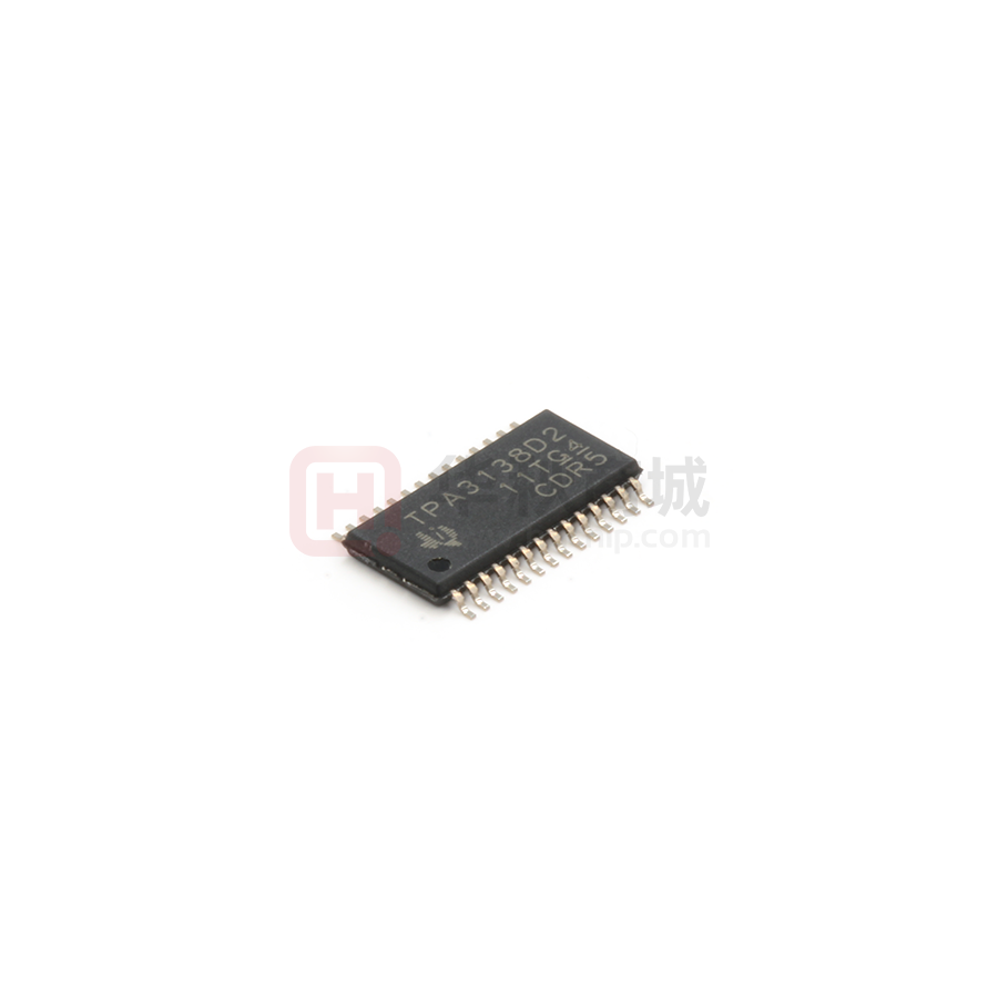
TPA3138D2
ZHCSHR9A – MARCH 2018 – REVISED JUNE 2018
TPA3138D2 10W、
、3.5V 至 14.4V、
、无电感器、立体声 D 类扬声器放大器
1 特性
•
1
•
•
•
•
•
2 应用
宽电源电压范围 3.5V 至 14.4V
– 6Ω、1% THD+N、12V 电源条件下,功率为 2
× 10W
– 4Ω、10% THD+N、12V 电源条件下,功率为 1
x 18.5W
– 1W、1kHz 输入、6Ω 条件下,THD+N 为
0.04%
电池寿命更长,适用于便携式 应用:
– 1SPW 模式下,空闲电流为 20mA (12V)
– >90% D 类效率
降低了解决方案尺寸和成本:
– 无电感器运行
– 不使用电感器时,符合 EN55013 和 EN55022
EMC 标准
– 无需外部散热器
灵活的音频解决方案:
– 单端或差动模拟输入
– 可选增益:20dB 和 26dB
– 启动时无喀哒声
综合保护和自动恢复:
– 引脚对引脚、引脚对地、引脚对电源短路保护
– 热保护、欠压保护和过压保护
– 功率限制器和直流扬声器保护
与 TPA3110D2、TPA3136D2 和 TPA3136AD2 引
脚对引脚兼容
•
•
•
•
•
电视和监控器
Bluetooth®扬声器和无线扬声器
智能设备中的音频放大器
物联网中的音频扬声器
消费类音频设备
3 说明
TPA3138D2 是一款每通道功率为 10W 的高效率、低
空闲电流 D 类立体声音频放大器。它可驱动负载低至
3.2Ω 的立体声扬声器。在 1SPW 模式下,它仅消耗
21mA (12V) 的低空闲电流,且可在低至 3.5V 条件下
运行,从而可实现更长的音频播放时间并改善蓝牙扬声
器、电池供电设备和其他功率敏感性应用中的 热性能
范围内实现精确性能。
利用扩频控制实现先进的 EMI 抑制功能,允许在满足
EMC 降低系统成本要求的同时,使用价格低廉的铁氧
体磁珠滤波器。
为了进一步简化设计,TPA3138D2 集成了重要的保护
特性, 包括欠压、过压、功率限制、短路、过热以及
直流扬声器保护。所有这些保护都可以自动恢复。
客户可以利用现有设计中的每个 TPA3138D2 特性,
因为它与 TI 的 TPA3110D2、TPA3136D2 和
TPA3136AD2 完全引脚对引脚兼容。
器件信息(1)
器件型号
封装
TPA3138D2
HTSSOP (28)
封装尺寸(标称值)
9.70mm × 4.40mm
(1) 如需了解所有可用封装,请参阅产品说明书末尾的可订购产品
附录。
简化原理图
采用铁氧体磁珠的 TPA3138 布局
TPA3138D2
Audio
Source
And Control
LEFT
PBTL
DETECT
FB
SD/FAULT
PVCC/AVCC
20dB/26dB GAIN Select
GAIN_SEL
Modulation Schemes/UV Level Select
MOD_SEL
Power Limit
Power Supply
3.5V t 14.4V
20.75 mm
FB
RIGHT
PLIMIT
20.50 mm
1
An IMPORTANT NOTICE at the end of this data sheet addresses availability, warranty, changes, use in safety-critical applications,
intellectual property matters and other important disclaimers. PRODUCTION DATA.
English Data Sheet: SLOS993
�TPA3138D2
ZHCSHR9A – MARCH 2018 – REVISED JUNE 2018
www.ti.com.cn
目录
1
2
3
4
5
6
7
8
9
特性 ..........................................................................
应用 ..........................................................................
说明 ..........................................................................
修订历史记录 ...........................................................
Device Comparison Table.....................................
Pin Configuration and Functions .........................
Specifications.........................................................
1
1
1
2
3
3
5
7.1
7.2
7.3
7.4
7.5
7.6
7.7
5
5
6
6
7
7
8
Absolute Maximum Ratings ......................................
ESD Ratings ............................................................
Recommended Operating Conditions.......................
Thermal Information ..................................................
Electrical Characteristics...........................................
Switching Characteristics ..........................................
Typical Characteristics ..............................................
Parameter Measurement Information ................ 10
Detailed Description ............................................ 11
9.1 Overview ................................................................. 11
9.2 Functional Block Diagram ....................................... 12
9.3 Feature Description................................................. 13
9.4 Device Functional Modes........................................ 16
10 Application and Implementation........................ 18
10.1 Application Information.......................................... 18
10.2 Typical Applications ............................................. 18
11 Power Supply Recommendations ..................... 25
11.1 Power Supply Decoupling, CS ............................. 25
12 Layout................................................................... 26
12.1 Layout Guidelines ................................................. 26
12.2 Layout Example .................................................... 27
13 器件和文档支持 ..................................................... 28
13.1
13.2
13.3
13.4
13.5
13.6
13.7
器件支持 ...............................................................
文档支持 ...............................................................
接收文档更新通知 .................................................
社区资源................................................................
商标 .......................................................................
静电放电警告.........................................................
术语表 ...................................................................
28
28
28
28
28
28
28
14 机械、封装和可订购信息 ....................................... 28
4 修订历史记录
注:之前版本的页码可能与当前版本有所不同。
Changes from Original (March 2018) to Revision A
Page
•
更改了器件状态:将“预告信息”更改成了“生产数据” ............................................................................................................... 1
2
Copyright © 2018, Texas Instruments Incorporated
�TPA3138D2
www.ti.com.cn
ZHCSHR9A – MARCH 2018 – REVISED JUNE 2018
5 Device Comparison Table
Product
Supply Voltage
Modulation Scheme
Package
Rdson
Gain
Inductor Free
TPA3138D2
3.5-V to 14.4-V
BD, 1SPW
HTSSOP-28
180-mΩ
20-dB, 26-dB
YES
TPA3110D2
8-V to 26-V
BD
HTSSOP-28
240-mΩ
20-dB, 26-dB, 32-dB, 36-dB
NO
TPA3136D2
4.5-V to 14.4-V
BD
HTSSOP-28
240-mΩ
26-dB
YES
TPA3136AD2
8-V to 14.4-V
BD
HTSSOP-28
240-mΩ
26-dB
YES
6 Pin Configuration and Functions
PWP Package
28-Pin HTSSOP
(Top View)
NC
1
28
PVCCL
SD/FAULT
2
27
PVCCL
LINP
3
26
BSPL
LINN
4
25
OUTPL
GAIN_SEL
5
24
GND
MODE_SEL
6
23
OUTNL
AVCC
7
22
BSNL
21
BSNR
Thermal
GND
8
GVDD
9
20
OUTNR
PLIMIT
10
19
GND
RINN
11
18
OUTPR
RINP
12
17
BSPR
NC
13
16
PVCCR
AGND
14
15
PVCCR
Pad
Not to scale
Pin Functions
PIN
NAME
NC
NO.
1
I/O/P (1)
DESCRIPTION
–
No Connect Pin. Can be shorted to PVCC or shorted to GND or left open.
TTL logic levels with compliance to AVCC. Shutdown logic input for audio amp (LOW , outputs Hi-Z;
HIGH , outputs enabled). General fault reporting including Over-Temp, Over-Current, DC Detect.
SD/FAULT= High, normal operation, SD/FAULT= Low, fault condition Device will auto-recover once
the OT/OC/DC Fault has been removed.
SD/FAULT
2
IO
LINP
3
I
Positive audio input for left channel. Biased at 2.5 V. Connect to GND for PBTL mode.
LINN
4
I
Negative audio input for left channel. Biased at 2.5 V. Connect to GND for PBTL mode.
GAIN_SEL
5
I
Gain select least significant bit. TTL logic levels with compliance to AVDD. Low = 20 dB Gain, High =
26 dB Gain, Floating = 26 dB Gain.
(1)
I = Input, O = Output, IO = Input and Output, P = Power
Copyright © 2018, Texas Instruments Incorporated
3
�TPA3138D2
ZHCSHR9A – MARCH 2018 – REVISED JUNE 2018
www.ti.com.cn
Pin Functions (continued)
PIN
NAME
NO.
I/O/P (1)
DESCRIPTION
MODE_SEL
6
I
Mode select least significant bit. TTL logic levels with compliance to AVDD. Low = BD Mode/UV
Threshold = 7.5 V, High = Low-Idle-Current 1SPW Mode/UV Threshold = 3.4V, Floating = Low-IdleCurrent 1SPW Mode/UV threshold = 3.4V
AVCC
7
P
Analog supply.
GND
8
–
Analog signal ground.
GVDD
9
O
FET gate drive supply. Nominal voltage is 5 V.
PLIMIT
10
I
Power limiter level control. Connect a resistor divider from GVDD to GND to set power limit. Connect
directly to GVDD for no power limit.
RINN
11
I
Negative audio input for right channel. Biased at 2.5 V.
RINP
12
I
Positive audio input for right channel. Biased at 2.5 V.
NC
13
–
No Connect Pin. Can be shorted to PVCC or shorted to GND or left open.
AGND
14
–
Analog signal ground. Connect to the thermal pad.
15, 16
P
Power supply for right channel H-bridge. Right channel and left channel power supply inputs are
connected internally.
PVCCR
BSPR
17
P
Bootstrap supply (BST) for right channel, positive high-side FET.
OUTPR
18
O
Class-D H-bridge positive output for right channel.
GND
19
–
Power ground for the H-bridges.
OUTNR
20
O
Class-D H-bridge negative output for right channel.
BSNR
21
P
Bootstrap supply (BST) for right channel, negative high-side FET.
BSNL
22
P
Bootstrap supply (BST) for left channel, negative high-side FET.
OUTNL
23
O
Class-D H-bridge negative output for left channel.
GND
24
–
Power ground for the H-bridges.
OUTPL
25
O
Class-D H-bridge positive output for left channel.
BSPL
26
P
Bootstrap supply (BST) for left channel, positive high-side FET.
27, 28
P
Power supply for left channel H-bridge. Right channel and left channel power supply inputs are
connected internally.
–
Connect to GND for best thermal and electrical performance
PVCCL
Thermal Pad
4
Copyright © 2018, Texas Instruments Incorporated
�TPA3138D2
www.ti.com.cn
ZHCSHR9A – MARCH 2018 – REVISED JUNE 2018
7 Specifications
7.1 Absolute Maximum Ratings
over operating free-air temperature range (unless otherwise noted) (1)
Supply voltage
AVCC to GND, PVCC to GND
Input current
To any pin except supply pins
SD/FAULT to GND (2), GAIN_SEL, MODE_SEL
Interface pin voltage
Minimum load resistance, RL
MIN
MAX
UNIT
–0.3
20
V
10
mA
–0.3
AVCC + 0.3
V
10
V/ms
PLIMIT
-0.3
GVDD + 0.3
V
RINN, RINP, LINN, LINP
–0.3
5.5
V
BTL, (10 V < PVCC < 14.4 V)
4.8
BTL, (3.5 V < PVCC < 10 V)
3.2
PBTL, (10 V < PVCC < 14.4 V)
2.4
PBTL, (3.5 V < PVCC < 10 V)
1.6
Ω
Continuous total power dissipation
See the Thermal
Information Table
Operating Juncation Temperature range
–25
150
°C
Storage temperature range, Tstg
–40
125
°C
(1)
(2)
Stresses beyond those listed under Absolute Maximum Ratings may cause permanent damage to the device. These are stress ratings
only, which do not imply functional operation of the device at these or any other conditions beyond those indicated under Recommended
Operating Conditions. Exposure to absolute-maximum-rated conditions for extended periods may affect device reliability.
The voltage slew rate of these pins must be restricted to no more than 10 V/ms. For higher slew rates, use a 100 kΩ resister in series
with the pins.
7.2 ESD Ratings
VALUE
V(ESD)
(1)
(2)
Electrostatic discharge
Human body model (HBM), per ANSI/ESDA/JEDEC JS-001
(1)
Charged device model (CDM), per JEDEC specification JESD22-C101
±1000
(2)
±250
UNIT
V
JEDEC document JEP155 states that 500-V HBM allows safe manufacturing with a standard ESD control process.
JEDEC document JEP157 states that 250-V CDM allows safe manufacturing with a standard ESD control process.
Copyright © 2018, Texas Instruments Incorporated
5
�TPA3138D2
ZHCSHR9A – MARCH 2018 – REVISED JUNE 2018
www.ti.com.cn
7.3 Recommended Operating Conditions
over operating free-air temperature range (unless otherwise noted)
PARAMETER
TEST CONDITIONS
MIN
MAX
UNIT
3.5
14.4
V
2
AVCC
V
VCC
Supply voltage
PVCC, AVCC
VIH
High-level input voltage
SD/FAULT
VIL
Low-level input voltage
SD/FAULT, GAIN_SEL, MODE_SEL (2)
0.8
V
VOL
Low-level output voltage
SD/FAULT, RPULL-UP =100 kΩ, PVCC = 14.4 V
0.8
V
IIH
High-level input current
SD/FAULT, GAIN_SEL, MODE_SEL, VI = 2 V, AVCC = 12 V
50
µA
IIL
Low-level input current
SD/FAULT, GAIN_SEL, MODE_SEL, VI = 0.8 V, AVCC = 12
V
5
µA
TA
Operating free-air temperature (3)
–10
85
°C
TJ
Operating junction temperature (3)
-10
150
°C
(1)
(2)
(3)
(1)
, GAIN_SEL, MODE_SEL
Set SD/FAULT to high level, make sure the pull-up resistor is larger than 4.7 kΩ and smaller than 500 kΩ
Set GAIN_SEL and MODE_SEL to low level, make sure pull down resistor


 工商网监
湘ICP备2023018690号
工商网监
湘ICP备2023018690号

