TPA6010A4
www.ti.com
SLOS268B – JUNE 2000 – REVISED AUGUST 2004
STEREO 2.7-W AUDIO POWER AMPLIFIER WITH BASS BOOST AND
DC VOLUME CONTROL
FEATURES
•
•
•
•
•
•
•
•
•
•
•
•
•
Compatible With PC 99 Desktop Line-Out Into
10-kΩ Load
Compatible With PC 99 Portable Into 8-Ω Load
Internal Gain Control, Which Eliminates
External Gain-Setting Resistors
DC Volume and Gain Control Adjustable From
34 dB to -86 dB
Bass Boost
Buffered Docking Station Outputs
2.7-W/Ch Output Power Into 3-Ω Load
PC-Beep Input
Depop Circuitry
Stereo Input MUX
Fully Differential Input
Low Supply Current and Shutdown Current
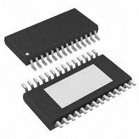
Surface-Mount Power Packaging 28-Pin
TSSOP PowerPAD™
PWP PACKAGE
(TOP VIEW)
GND
LOUT−
BBENABLE
BYPASS
LIN
LHPIN
LLINEIN
PC-BEEP
RLINEIN
RHPIN
RIN
SHUTDOWN
HP/LINE
ROUT−
1
2
3
4
5
6
7
8
9
10
11
12
13
14
28
27
26
25
24
23
22
21
20
19
18
17
16
15
LOUT+
CLK
LDOCKOUT
PVDD
BUFFGAIN
VOLUME
VDD
BBIN
BBOUT
PVDD
RDOCKOUT
SE/BTL
ROUT+
GND
DESCRIPTION
The TPA6010A4 is a stereo audio power amplifier in a 28-pin TSSOP thermally enhanced package capable of
delivering 2.7 W of continuous RMS output power into 3-Ω loads. When driving 1 W into 8-Ω speakers, the
TPA6010A4 has less than 0.22% THD+N across its specified frequency range.
The TPA6010A4 has several features optimized for notebook PCs including bass boost, docking station outputs,
dc volume control, and dc gain control.
The TPA6010A4 has a buffer and volume control gain stage that are set by dc voltages. The buffer has a
differential input and a differential output. The gain of the buffer, which is controlled by the dc voltage on the
BUFFGAIN terminal, is adjustable from -46 dB to 14 dB. The docking station output is 6 dB lower than the buffer
gain because the buffer has a differential output and the docking station output is taken from just one of the
buffer outputs. The volume control amplifier is adjustable from -34 dB to 20 dB in BTL mode and is 6 dB lower in
SE mode. The volume control stage is adjustable by dc voltage on the VOLUME terminal. The amplifier gain
from input-to-speaker is the sum of the volume control and the buffer gain. The input-to-speaker gain is
adjustable from -86 dB to 34 dB in BTL mode and -92 dB to 28 dB in the SE mode.
The bass boost of the amplifier sums the right and left inputs, adds gain, filters out the high frequencies, and
then adds the bass boost signal back into the output power amplifier. The frequency of the bass boost is
adjusted by adding an RC filter from BBOUT to BBIN. The gain of the bass boost is set to 12 dB if the same
bass is present in both the right and left channels. If the bass is present in just one of the channels, the gain of
the bass is set to 9.5 dB. The gain can be reduced by adding a voltage divider from BBIN to BBOUT. If not using
the bass boost, pull the BBENABLE pin low.
Please be aware that an important notice concerning availability, standard warranty, and use in critical applications of Texas
Instruments semiconductor products and disclaimers thereto appears at the end of this data sheet.
PowerPAD is a trademark of Texas Instruments.
PRODUCTION DATA information is current as of publication date.
Products conform to specifications per the terms of the Texas
Instruments standard warranty. Production processing does not
necessarily include testing of all parameters.
Copyright © 2000–2004, Texas Instruments Incorporated
�TPA6010A4
www.ti.com
SLOS268B – JUNE 2000 – REVISED AUGUST 2004
The PowerPAD package (PWP) delivers a level of thermal performance that was previously achievable only in
TO-220-type packages. Thermal impedances of approximately 35°C/W are truly realized in multilayer PCB
applications. This allows the TPA6010A4 to operate at full power into 8-Ω loads at ambient temperatures of
85°C.
FUNCTIONAL BLOCK DIAGRAM
BUFFGAIN
RHPIN
RLINEIN
RIN
R
MUX
RDOCKOUT
VOLUME
−
−
+
+
Σ
−
ROUT+
+
−
Σ
BUFFGAIN
VOLUME
CLK
VDD
ROUT−
DC GAIN
and Volume
Control
Σ
PVDD
BYPASS
+
−
BBOUT
+
Power
Management
Bass
Boost
Σ
SHUTDOWN
RBB
GND
−
PC-BEEP
SE/BTL
HP/LINE
LHPIN
LLINEIN
LIN
BBIN
+
PC
BEEP
CBB
MUX
CONTROL
L
MUX
BBENABLE
−
−
+
+
BUFFGAIN
Σ
−
+
LOUT+
VOLUME
−
Σ
LOUT−
+
LDOCKOUT
2
�TPA6010A4
www.ti.com
SLOS268B – JUNE 2000 – REVISED AUGUST 2004
These devices have limited built-in ESD protection. The leads should be shorted together or the device
placed in conductive foam during storage or handling to prevent electrostatic damage to the MOS gates.
AVAILABLE OPTIONS
PACKAGED DEVICE
TA
TSSOP (1) (PWP)
-40°C to 85°C
(1)
TPA6010A4PWP
The PWP package is available taped and reeled. To order a taped
and reeled part, add the suffix R to the part number (e.g.,
TPA6010A4PWPR).
Terminal Functions
TERMINAL
NAME
NO.
I/O
DESCRIPTION
BBENABLE
3
I
BBENABLE is the bass boost control input. When this terminal is held high, the extra bass from the bass
boost circuitry is added to the output signal. When this terminal is held low, no extra bass is added.
BBIN
21
I
BBIN is the buffered input to the power amplifier from the bass boost circuitry.
BBOUT
20
O
BBOUT is the bass boost output. A low pass filter must be placed from BBOUT to BBIN to select the low
frequencies to be boosted.
BYPASS
4
CLK
27
I
If a 47-nF capacitor is attached, the TPA6010A4 generates an internal clock. An external clock can
override the internal clock input to this terminal.
BUFFGAIN
24
I
The gain of the dockout buffer is adjustable from -52 dB to 8 dB to LDOCKOUT and RDOCKOUT, and is
set by a dc voltage from 0 V to 3.54 V. When the dc level is over 3.54 V, the device is muted.
GND
Tap to voltage divider for internal midsupply bias generator
1, 15
Ground connection for circuitry. Connected to thermal pad.
HP/LINE
13
I
MUX control input, hold high to select LHPIN or RHPIN, hold low to select LLINEIN or RLINEIN.
LHPIN
6
I
Left channel headphone input, selected when HP/LINE is held high
LIN
5
I
Common left input for fully differential input. AC ground for single-ended inputs
LLINEIN
7
I
Left channel line negative input, selected when HP/LINE is held low
LDOCKOUT
26
O
LDOCKOUT is the buffered output of LLINEIN or LHPIN. Use BUFFGAIN for volume adjustment of this
pin.
LOUT+
28
O
Left channel positive output in BTL mode and positive output in SE mode
LOUT-
2
O
Left channel negative output in BTL mode and high-impedance in SE mode
PC-BEEP
8
I
The input for PC Beep mode. PC-BEEP is enabled when a > 1.5-V (peak-to-peak) square wave is input to
PC-BEEP. AC ground if use is not desired.
PVDD
19, 25
I
Power supply for output stage
RHPIN
10
I
Right channel headphone input, selected when HP/LINE is held high
RIN
11
I
Common right input for fully differential input. AC ground for single-ended inputs
RLINEIN
9
I
Right channel line input, selected when HP/LINE is held low
RDOCKOUT
18
O
RDOCKOUT is the buffered output of RLINEIN or RHPIN. Use BUFFGAIN for volume adjustment of this
pin.
ROUT+
16
O
Right channel positive output in BTL mode and positive output in SE mode
ROUT-
14
O
Right channel negative output in BTL mode and high-impedance in SE mode
SE/BTL
17
I
Output MUX control. When this terminal is high, SE outputs are selected. When this terminal is low, the
BTL outputs are selected.
SHUTDOWN
12
I
When held low, this terminal places the entire device, except PC-BEEP detect circuitry, in shutdown mode.
VDD
22
I
Analog VDD input supply. This terminal needs to be isolated from PVDD to achieve highest performance.
VOLUME
23
I
VOLUME detects the dc level at the terminal and sets the gain for 31 discrete steps covering a range of 20
dB to -40 dB for dc levels of 0.15 V to 3.54. When the dc level is over 3.54 V, the device is muted.
Thermal Pad
Connect to GND. The pad must be soldered down in all applications in order to properly secure the device
to the PCB.
3
�TPA6010A4
www.ti.com
SLOS268B – JUNE 2000 – REVISED AUGUST 2004
ABSOLUTE MAXIMUM RATINGS
over operating free-air temperature range (unless otherwise noted) (1)
UNIT
VDD
Supply voltage
VI
Input voltage
6V
-0.3 V to VDD +0.3 V
Continuous total power dissipation
Internally Limited (see Dissipation Rating Table)
TA
Operating free-air temperature range
-40°C to 85°C
TJ
Operating junction temperature range
-40°C to 150°C
Tstg
Storage temperature range
-65°C to 85°C
Lead temperature 1,6 mm (1/16 inch) from case for 10 seconds
(1)
260°C
Stresses beyond those listed under "absolute maximum ratings" may cause permanent damage to the device. These are stress ratings
only, and functional operation of the device at these or any other conditions beyond those indicated under "recommended operating
conditions" is not implied. Exposure to absolute-maximum-rated conditions for extended periods may affect device reliability.
DISSIPATION RATING TABLE
PACKAGE
TA ≤ 25°C
DERATING FACTOR
TA = 70°C
TA = 85°C
PWP
2.7 W (1)
21.8 mW/°C
1.7 W
1.4 W
(1)
See the Texas Instruments document, PowerPAD Thermally Enhanced Package Application Report (SLMA002), for more information on
the PowerPAD™ package. The thermal data was measured on a PCB layout based on the information in the section entitled Texas
Instruments Recommended Board for PowerPAD on page 33 of the before mentioned document.
RECOMMENDED OPERATING CONDITIONS
VDD
Supply voltage
High-level input voltage
VIL
Low-level input voltage
TA
Operating free-air temperature
MAX
4.5
5.5
0.8 × VDD
SE/BTL, HP/LINE
VIH
MIN
SHUTDOWN, BBENABLE
0.6 × VDD
SHUTDOWN, BBENABLE
0.8
-40
V
V
2
SE/BTL, HP/LINE
UNIT
85
V
°C
ELECTRICAL CHARACTERISTICS
at specified free-air temperature, VDD = 5 V, TA = 25°C (unless otherwise noted)
PARAMETER
|VOS|
Output offset voltage (measured differentially)
PSRR Power supply rejection ratio
|IIH|
High-level input current
SHUTDOWN, SE/BTL, HP/LINE,
VOLUME, BUFFGAIN, BBENABLE
|IIL|
Low-level input current
SHUTDOWN, SE/BTL, HP/LINE,
VOLUME, BUFFGAIN, BBENABLE
IDD
Supply current
IDD(SD) Supply current, shutdown mode
4
TEST CONDITIONS
MIN
TYP
AV = 6 dB
VDD = 4.9 V to 5.1 V
MAX
35
67
UNIT
mV
dB
VDD = 5.5 V, VI = VDD
1
µA
VDD = 5.5 V, VI = 0 V
1
µA
BTL mode, SHUTDOWN = 2 V,
SE/BTL = 0.6 × VDD
12
18
SE mode, SHUTDOWN = 2 V,
SE/BTL = 0.8 × VDD
6.5
10
PC-BEEP = 2.5 V,
SHUTDOWN = 0 V
95
250
PC-BEEP = 0 V,
SHUTDOWN = 0 V
62
200
mA
µA
�TPA6010A4
www.ti.com
SLOS268B – JUNE 2000 – REVISED AUGUST 2004
OPERATING CHARACTERISTICS
VDD = 5 V, TA = 25°C, RL = 4 Ω, Gain = 6 dB, BTL mode (unless otherwise noted)
PARAMETER
TEST CONDITIONS
PO
Output power
RL = 3 Ω, f = 1 kHz
THD + N
Total harmonic distortion plus noise
PO = 1 W,
BOM
Bandwidth, maximum output power
THD = 1%
kSVR
Supply ripple rejection ratio
f = 20 Hz to 20 kHz,
CBypass = 1 µF, Vripple = 200 mVpp
Vn
Output noise voltage
xtalk
Crosstalk
MIN
TYP MAX
THD = 10%
2.7
THD = 1%
2.2
f = 20 Hz to 15 kHz
UNIT
W
0.45%
>15
kHz
BTL mode
56
dB
CBypass = 1 µF,
f = 20 Hz to 20 kHz
BTL mode
50
SE mode
32
f = 20 Hz to 20 kHz
BTL mode
-80
µVRMS
dB
OPERATING CHARACTERISTICS
VDD = 5 V, TA = 25°C, RL = 8 Ω, Gain = 6 dB, BTL mode (unless otherwise noted)
PARAMETER
TEST CONDITIONS
MIN
TYP
1
MAX
UNIT
PO
Output power
THD = 0.06%,
f = 1 kHz
THD + N
Total harmonic distortion plus noise
PO = 0.5 W,
f = 20 Hz to 15 kHz
W
BOM
Bandwidth, maximum output power
THD = 1%
>15
kHz
kSVR
Supply ripple rejection ratio
f = 20 Hz to 20 kHz,
BTL mode
CBypass = 1 µF, Vripple = 200 mVpp
56
dB
Vn
Output noise voltage
CB = 1 µF,
f = 20 Hz to 20 kHz
BTL mode
50
SE mode
32
xtalk
Crosstalk
f = 20 Hz to 20 kHz
BTL mode
-80
0.5%
µVRMS
dB
5
�TPA6010A4
www.ti.com
SLOS268B – JUNE 2000 – REVISED AUGUST 2004
TYPICAL CHARACTERISTICS
Table of Graphs
FIGURE
vs Output power
THD + N
Total harmonic distortion + noise
1,2
vs Dockout voltage
3
vs Frequency
4, 5, 6
TOTAL HARMONIC DISTORTION + NOISE
vs
OUTPUT POWER
TOTAL HARMONIC DISTORTION + NOISE
vs
OUTPUT POWER
10
VDD = 5 V,
f = 1 kHz
Bridge-Tied Load
Gain = 6 dB
1
RL = 3 Ω
RL = 4 Ω
0.1
RL = 8 Ω
0.01
0.01
0.1
PO − Output Power − W
Figure 1.
6
THD+N − Total Harmonic Distortion + Noise − %
THD+N − Total Harmonic Distortion + Noise − %
10
1
2
3
VDD = 5 V,
f = 1 kHz
RL = 32 Ω
Single-Ended
Gain = 6 dB
1
0.1
0.01
10
100
50
PO − Output Power − mW
Figure 2.
200
�TPA6010A4
www.ti.com
SLOS268B – JUNE 2000 – REVISED AUGUST 2004
TOTAL HARMONIC DISTORTION + NOISE
vs
DOCKOUT VOLTAGE
TOTAL HARMONIC DISTORTION + NOISE
vs
FREQUENCY
THD+N − Total Harmonic Distortion + Noise − %
1
0.1
0.01
THD+N − Total Harmonic Distortion + Noise − %
10
VDD = 5 V,
RL = 10 kΩ
f = 1 kHz
Gain = 6 dB
0.1
0.5
1
VO − Dockout Voltage − V
VDD = 5 V,
Bridge-Tied Load
Gain = 6 dB
RL = 3 Ω,
PO = 2 W
RL = 4 Ω,
PO = 1.5 W
1
RL = 8 Ω,
PO = 1 W
0.1
0.01
2
20
100
1k
f − Frequency − Hz
10 k 20 k
Figure 3.
Figure 4.
TOTAL HARMONIC DISTORTION + NOISE
vs
FREQUENCY
TOTAL HARMONIC DISTORTION + NOISE
vs
FREQUENCY
1
1
THD+N − Total Harmonic Distortion + Noise − %
THD+N − Total Harmonic Distortion + Noise − %
10
VDD = 5 V,
Gain = 6 dB
Single-Ended
RL = 32 Ω
PO = 75 mW
0.1
0.01
0.001
20
100
1k
f − Frequency − Hz
Figure 5.
10 k 20 k
VDD = 5 V,
CI = 0.47 µF,
RL = 10 kΩ
Gain = 6 dB,
Dockout
VO = 1 Vrms
0.1
VO = 500 mVrms
0.01
20
100
1k
f − Frequency − Hz
10 k 20 k
Figure 6.
7
�TPA6010A4
www.ti.com
SLOS268B – JUNE 2000 – REVISED AUGUST 2004
APPLICATION INFORMATION
INTERNAL BUFFER GAIN AND VOLUME GAIN
The typical voltage and gain levels are shown in Table 1 and Table 2.
Table 1. BUFFGAIN Voltage and Gain Values
TYPICAL GAIN OF AMPLIFIER (VOLUME Stage) (1)
BUFFGAIN (Terminal 24)
Inceasing Voltage
(1)
(2)
(3)
8
(V) (2) (3)
Decreasing Voltage
(V) (2) (3)
Internal Gain (dB)
DOCKOUT Gain (dB)
0.00 – 0.20
0.16 – 0.00
14
8
0.21 – 0.31
0.27 – 0.17
12
6
0.32 – 0.42
0.38 – 0.28
10
4
0.43 – 0.54
0.50 – 0.39
8
2
0.55 – 0.65
0.61 – 0.51
6
0
0.66 – 0.76
0.72 – 0.62
4
-2
0.77 – 0.88
0.84 – 0.73
2
-4
0.89 – 0.99
0.96 – 0.85
0
-6
1.00 – 1.11
1.07 – 0.97
-2
-8
1.12 – 1.22
1.19 – 1.08
-4
-10
1.23 – 1.34
1.30 – 1.20
-6
-12
1.35 – 1.45
1.42 – 1.31
-8
-14
1.46 – 1.56
1.53 – 1.43
-10
-16
1.57 – 1.68
1.64 – 1.54
-12
-18
1.69 – 1.79
1.76 – 1.65
-14
-20
1.80 – 1.91
1.88 – 1.77
-16
-22
1.92 – 2.02
1.99 – 1.89
-18
-24
2.03 – 2.14
2.11 – 2.00
-20
-26
2.15 – 2.25
2.23 – 2.12
-22
-28
2.26 – 2.37
2.34 – 2.24
-24
-30
2.38 – 2.48
2.47 – 2.35
-26
-32
2.49 – 2.60
2.57 – 2.46
-28
-34
2.61 – 2.71
2.69 – 2.58
-30
-36
2.72 – 2.83
2.81 – 2.70
-32
-38
2.84 – 2.95
2.92 – 2.82
-34
-40
2.96 – 3.06
3.04 – 2.93
-36
-42
3.07 – 3.18
3.15 – 3.05
-38
-44
3.19 – 3.29
3.27 – 3.16
-40
-46
3.30 – 3.41
3.39 – 3.28
-42
-48
3.42 – 3.52
3.50 – 3.40
-44
-50
3.53 – 3.63
3.62 – 3.51
-46
-52
3.64 – 5.00
5.00 – 3.63
-75
-81
Typical gain values can vary by ±2 dB.
To set the Internal and DOCKOUT gain to a fixed value upon power up, use the appropriate voltage range in the Decreasing Voltage
column.
For best results, set the voltage to the middle of the appropriate voltage range.
�TPA6010A4
www.ti.com
SLOS268B – JUNE 2000 – REVISED AUGUST 2004
Table 2. VOLUME Voltage and Gain Values
TYPICAL GAIN OF AMPLIFIER (VOLUME Stage) (1)
VOLUME (Terminal 23)
Inceasing Voltage
(1)
(2)
(3)
(V) (2) (3)
Decreasing Voltage
(V) (2) (3)
BTL Gain (dB)
SE Gain (dB)
0.00 – 0.20
0.16 – 0.00
20
14
0.21 – 0.31
0.27 – 0.17
18
12
0.32 – 0.42
0.38 – 0.28
16
10
0.43 – 0.54
0.50 – 0.39
14
8
0.55 – 0.65
0.61 – 0.51
12
6
0.66 – 0.76
0.72 – 0.62
10
4
0.77 – 0.88
0.84 – 0.73
8
2
0.89 – 0.99
0.96 – 0.85
6
0
1.00 – 1.11
1.07 – 0.97
4
-2
1.12 – 1.22
1.19 – 1.08
2
-4
1.23 – 1.34
1.30 – 1.20
0
-6
1.35 – 1.45
1.42 – 1.31
-2
-8
1.46 – 1.56
1.53 – 1.43
-4
-10
1.57 – 1.68
1.64 – 1.54
-6
-12
1.69 – 1.79
1.76 – 1.65
-8
-14
1.80 – 1.91
1.88 – 1.77
-10
-16
1.92 – 2.02
1.99 – 1.89
-12
-18
2.03 – 2.14
2.11 – 2.00
-14
-20
2.15 – 2.25
2.23 – 2.12
-16
-22
2.26 – 2.37
2.34 – 2.24
-18
-24
2.38 – 2.48
2.47 – 2.35
-20
-26
2.49 – 2.60
2.57 – 2.46
-22
-28
2.61 – 2.71
2.69 – 2.58
-24
-30
2.72 – 2.83
2.81 – 2.70
-26
-32
2.84 – 2.95
2.92 – 2.82
-28
-34
2.96 – 3.06
3.04 – 2.93
-30
-36
3.07 – 3.18
3.15 – 3.05
-32
-38
3.19 – 3.29
3.27 – 3.16
-34
-40
3.30 – 3.41
3.39 – 3.28
-36
-42
3.42 – 3.52
3.50 – 3.40
-38
-44
3.53 – 3.63
3.62 – 3.51
-40
-46
3.64 – 5.00
5.00 – 3.63
-95
-95
Typical gain values can vary by ±2 dB.
To set the Internal and DOCKOUT gain to a fixed value upon power up, use the appropriate voltage range in the Decreasing Voltage
column.
For best results, set the voltage to the middle of the appropriate voltage range.
The total gain of the amplifier can be determined using the following equations:
Total gain = Internal gain (dB) + BTL gain (dB), if outputs are bridge-tied.
Total gain = Internal gain (dB) + SE gain (dB), if outputs are single-ended.
9
�TPA6010A4
www.ti.com
SLOS268B – JUNE 2000 – REVISED AUGUST 2004
CRHP
0.47 µF
Right
Headphone
Input Signal
RDOCKOUT
CRLINE
Right Line
Input Signal
0.47 µF
CRIN
0.47 µF
VDD
50 kΩ
VDD
10
9
11
RHPIN
RLINEIN
RIN
24
BUFFGAIN
23
27
VOLUME
CLK
R
MUX
BUFFGAIN
VOLUME
−
−
+
+
Σ
−
Σ
DC GAIN
and Volume
Control
ROUT− 14
See Note A
CSR
0.1 µF
VDD
CSR
0.1 µF
CBYP
0.47 µF
VDD
Left
Headphone
Input Signal
1 kΩ
100 kΩ
19, 25 PVDD
22 VDD
4 BYPASS
12 SHUTDOWN
1, 15
Σ
−
BBOUT 20
+
Power
Management
Depop
Circuitry
Bass
Boost
Σ
RBB
GND
−
To System
Control
PC Beep
Input Signal
COUTR
100 µF
+
50 kΩ
VDD
To Right Docking
Station Input
See Note B
ROUT+ 16
+
−
CCLK
47 nF
18
CPCB
0.47 µF
CLHP
0.47 µF
CLLINE
0.47 µF
Left Line
Input Signal
8
PC-BEEP
17
13
SE/BTL
HP/LINE
6
7
5
LHPIN
LLINEIN
LIN
PC
BEEP
BBENABLE
−
+
BUFFGAIN
CLIN
0.47 µF
21
CBB
MUX
CONTROL
L
MUX
BBIN
+
Σ
−
+
−
3
1 kΩ
COUTL
100 µF
To System
Control
LOUT+ 28
+
VOLUME
−
Σ
LOUT− 2
+
LDOCKOUT
26
100 kΩ
To Left Docking
Station Input
See Note B
A.
A 0.1-µF ceramic capacitor should be placed as close as possible to the IC. For filtering lower-frequency noise
signals, a larger electrolytic capacitor of 10 µF or greater should be placed near the audio power amplifier.
B.
A DC-blocking capacitor should be placed at each input to the amplifier in the docking station, as the RDOCKOUT
and LDOCKOUT pins are biased to VDD/2.
Figure 7. Typical TPA6010A4 Application Circuit Using Single-Ended Inputs and Input MUX
10
�TPA6010A4
www.ti.com
SLOS268B – JUNE 2000 – REVISED AUGUST 2004
N/C
Right Positive
Differential
Input Signal
RDOCKOUT 18
CRIN−
0.47 µF
Right Negative
Differential
Input Signal
10 RHPIN
9 RLINEIN
11 RIN
R
MUX
BUFFGAIN
CRIN+
0.47 µF
VDD
50 kΩ
VDD
VOLUME
−
−
+
+
Σ
−
23 VOLUME
27 CLK
CCLK
47 nF
ROUT+ 16
+
−
24 BUFFGAIN
Σ
DC GAIN
and Volume
Control
ROUT− 14
See Note A
VDD
VDD
CSR
0.1 µF
CBYP
0.47 µF
BYPASS
SHUTDOWN
CPCB
0.47 µF
N/C
Left Positive
Differential
Input Signal
−
BBOUT
20
+
Power
Management
Depop
Circuitry
Bass
Boost
Σ
RBB
1, 15 GND
8 PC-BEEP
Left Negative
Differential
Input Signal
Σ
PVDD
VDD
−
To System
Control
PC Beep
Input Signal
1 kΩ
100 kΩ
19, 25
22
4
12
CSR
0.1 µF
COUTR
100 µF
+
50 kΩ
VDD
To Right Docking
Station Input
See Note B
CLIN−
0.47 µF
17 SE/BTL
13 HP/LINE
6 LHPIN
7 LLINEIN
5 LIN
BBIN
+
PC
BEEP
CBB
MUX
CONTROL
L
MUX
CLIN+
0.47 µF
21
BBENABLE
−
−
+
+
BUFFGAIN
Σ
−
3
1 kΩ
COUTL
100 µF
To System
Control
LOUT+ 28
+
VOLUME
−
Σ
LOUT− 2
+
LDOCKOUT 26
100 kΩ
To Left Docking
Station Input
See Note B
A.
A 0.1-µF ceramic capacitor should be placed as close as possible to the IC. For filtering lower-frequency noise
signals, a larger electrolytic capacitor of 10 µF or greater should be placed near the audio power amplifier.
B.
A DC-blocking capacitor should be placed at each input to the amplifier in the docking station, as the RDOCKOUT
and LDOCKOUT pins are biased to VDD/2.
Figure 8. Typical TPA6010A4 Application Circuit Using Differential Inputs
INPUT RESISTANCE
Each gain setting is achieved by varying the input resistance of the amplifier, which can range from its smallest
value to over 6 times that value. As a result, if a single capacitor is used in the input high pass filter, the -3 dB or
cut-off frequency also changes by over 6 times.
RF
C
Input Signal
IN
RI
Figure 9. Resistor-On Input for Cut-Off Frequency
11
�TPA6010A4
www.ti.com
SLOS268B – JUNE 2000 – REVISED AUGUST 2004
INPUT CAPACITOR, CI
In the typical application an input capacitor, CI, is required to allow the amplifier to bias the input signal to the
proper dc level for optimum operation. In this case, CI and the input resistance of the amplifier, RI, form a
high-pass filter with the corner frequency determined in Equation 1.
-3 dB
fc �
1
2 � RI C I
fc
(1)
The value of CI is important to consider as it directly affects the bass (low frequency) performance of the circuit.
Consider the example where RI is 70 kΩ and the specification calls for a flat bass response down to 40 Hz.
Equation 1 is reconfigured as Equation 2.
CI �
1
2 � RI f c
(2)
In this example, CI is 5.6 nF so one would likely choose a value in the range of 5.6 nF to 1 µF. A further
consideration for this capacitor is the leakage path from the input source through the input network (CI) and the
feedback network to the load. This leakage current creates a dc offset voltage at the input to the amplifier that
reduces useful headroom, especially in high gain applications. For this reason a low-leakage tantalum or ceramic
capacitor is the best choice. When polarized capacitors are used, the positive side of the capacitor should face
the amplifier input in most applications as the dc level there is held at VDD/2, which is likely higher than the
source dc level. Note that it is important to confirm the capacitor polarity in the application.
POWER SUPPLY DECOUPLING, CS
The TPA6010A4 is a high-performance CMOS audio amplifier that requires adequate power supply decoupling to
ensure the output total harmonic distortion (THD) is as low as possible. Power supply decoupling also prevents
oscillations for long lead lengths between the amplifier and the speaker. The optimum decoupling is achieved by
using two capacitors of different types that target different types of noise on the power supply leads. For higher
frequency transients, spikes, or digital hash on the line, a good low equivalent-series-resistance (ESR) ceramic
capacitor, typically 0.1 µF placed as close as possible to the device VDD lead works best. For filtering
lower-frequency noise signals, a larger aluminum electrolytic capacitor of 10 µF or greater placed near the audio
power amplifier is recommended.
MIDRAIL BYPASS CAPACITOR, CBYP
The midrail bypass capacitor, CBYP, is the most critical capacitor and serves several important functions. During
startup or recovery from shutdown mode, CBYP determines the rate at which the amplifier starts up. The second
function is to reduce noise produced by the power supply caused by coupling into the output drive signal. This
noise is from the midrail generation circuit internal to the amplifier, which appears as degraded PSRR and
THD+N.
For the bypass capacitor, CBYP, 0.47 µF to 1 µF ceramic or tantalum low-ESR capacitors are recommended for
the best THD and noise performance.
12
�TPA6010A4
www.ti.com
SLOS268B – JUNE 2000 – REVISED AUGUST 2004
BASS BOOST OPERATION
The bass boost feature of the TPA6010A4 sums the left and right inputs, adds gain, filters out the high
frequencies, and adds the bass-boosted signal back into the current-gain stage of the amplifier. The cutoff
frequency is set by RBB and CBB as shown in Equation 3.
-3 dB
fc �
1
2� R
C
BB BB
fc
(3)
The gain of the bass boost is set internally at 12 dB if bass is present in both the right and left channels. If bass
is only present in one of the channels, the boost is reduced to 9.5 dB.
The total bass boost gain may be determined by using Equation 4.
Bass Boost Gain � 12 dB � 20Log
�R1 R2
�
� R2
Bass Boost Gain � 9.5 dB � 20Log
(bass present on both channels)
�R1 R2
�
� R2
(bass present on only one channel)
(4)
Consider the following example application. The desired cutoff frequency for the bass boost is 300 Hz and the
desired bass boost gain is 6 dB. The filter components could be RBB = 1.1 kΩ and CBB = 0.47 µF.
If the bass boost feature is not to be used or if the user wishes to disable the boost, the BBENABLE pin should
be pulled low.
Finally, as illustrated in the functional block diagram, the bass boost is only applied to the speaker outputs, not to
the docking station outputs.
OUTPUT COUPLING CAPACITOR, CC
In the typical single-supply SE configuration, an output coupling capacitor (CC) is required to block the dc bias at
the output of the amplifier thus preventing dc currents in the load. As with the input coupling capacitor, the output
coupling capacitor and impedance of the load form a high-pass filter governed by Equation 5.
-3 dB
fc �
1
2 � RL C C
fc
(5)
The main disadvantage, from a performance standpoint, is the load impedances are typically small, which drives
the low-frequency corner higher degrading the bass response. Large values of CC are required to pass low
frequencies into the load. Consider the example where a CC of 330 µF is chosen and loads vary from 3 Ω, 4 Ω, 8
Ω, 32Ω , 10 kΩ, and 47 kΩ. Table 3 summarizes the frequency response characteristics of each configuration.
13
�TPA6010A4
www.ti.com
SLOS268B – JUNE 2000 – REVISED AUGUST 2004
Table 3. Common Load Impedances vs Low Frequency Output Characteristics
in SE Mode
RL
CC
LOWEST FREQUENCY
3Ω
330 µF
161 Hz
4Ω
330 µF
120 Hz
8Ω
330 µF
60 Hz
32 Ω
330 µF
15 Hz
10,000 Ω
330 µF
0.05 Hz
47,000 Ω
330 µF
0.01 Hz
As Table 3 indicates, most of the bass response is attenuated into a 4-Ω load, an 8-Ω load is adequate,
headphone response is good, and drive into line level inputs (a home stereo for example) is exceptional.
USING LOW-ESR CAPACITORS
Low-ESR capacitors are recommended throughout this applications section. A real (as opposed to ideal)
capacitor can be modeled simply as a resistor in series with an ideal capacitor. The voltage drop across this
resistor minimizes the beneficial effects of the capacitor in the circuit. The lower the equivalent value of this
resistance the more the real capacitor behaves like an ideal capacitor.
BRIDGED-TIED LOAD VERSUS SINGLE-ENDED MODE
Figure 10 shows a Class-AB audio power amplifier (APA) in a BTL configuration. The TPA6010A4 BTL amplifier
consists of two Class-AB amplifiers driving both ends of the load. There are several potential benefits to this
differential drive configuration but initially consider power to the load. The differential drive to the speaker means
that as one side is slewing up, the other side is slewing down, and vice versa. This in effect doubles the voltage
swing on the load as compared to a ground referenced load. Plugging 2 × VO(PP) into the power equation, where
voltage is squared, yields 4× the output power from the same supply rail and load impedance as in Equation 6.
V(rms) �
Power �
V O(PP)
2 �2
V(rms)
2
RL
(6)
VDD
VO(PP)
RL
2x VO(PP)
VDD
-VO(PP)
Figure 10. Bridge-Tied Load Configuration
14
�TPA6010A4
www.ti.com
SLOS268B – JUNE 2000 – REVISED AUGUST 2004
In a typical computer sound channel operating at 5 V, bridging raises the power into an 8-Ω speaker from a
singled-ended (SE, ground reference) limit of 250 mW to 1 W. In sound power that is a 6-dB improvement —
which is loudness that can be heard. In addition to increased power there are frequency response concerns.
Consider the single-supply SE configuration shown in Figure 11. A coupling capacitor is required to block the dc
offset voltage from reaching the load. These capacitors can be quite large (approximately 33 µF to 1000 µF) so
they tend to be expensive, heavy, occupy valuable PCB area, and have the additional drawback of limiting
low-frequency performance of the system. This frequency limiting effect is due to the high-pass filter network
created with the speaker impedance and the coupling capacitance and is calculated with Equation 7.
fc �
1
2 � RL C C
(7)
For example, a 68-µF capacitor with an 8-Ω speaker would attenuate low frequencies below 293 Hz. The BTL
configuration cancels the dc offsets, which eliminates the need for the blocking capacitors. Low-frequency
performance is then limited only by the input network and speaker response. Cost and PCB space are also
minimized by eliminating the bulky coupling capacitor.
VDD
-3 dB
VO(PP)
CC
RL
VO(PP)
fc
Figure 11. Single-Ended Configuration and Frequency Response
Increasing power to the load does carry a penalty of increased internal power dissipation. The increased
dissipation is understandable considering that the BTL configuration produces 4× the output power of the SE
configuration. Internal dissipation versus output power is discussed further in the CREST FACTOR and
THERMAL CONSIDERATIONS section.
SINGLE-ENDED OPERATION
In SE mode (see Figure 10 and Figure 11), the load is driven from the primary amplifier output for each channel
(OUT+, terminals 28 and 16).
The amplifier switches single-ended operation when the SE/BTL terminal is held high. This puts the negative
outputs in a high-impedance state, and reduces the amplifier's gain to 1 V/V.
BTL AMPLIFIER EFFICIENCY
Class-AB amplifiers are notoriously inefficient. The primary cause of these inefficiencies is voltage drop across
the output stage transistors. There are two components of the internal voltage drop. One is the headroom or dc
voltage drop that varies inversely to output power. The second component is due to the sinewave nature of the
output. The total voltage drop can be calculated by subtracting the RMS value of the output voltage from VDD.
The internal voltage drop multiplied by the RMS value of the supply current, IDDrms, determines the internal
power dissipation of the amplifier.
An easy-to-use equation to calculate efficiency starts out being equal to the ratio of power from the power supply
to the power delivered to the load. To accurately calculate the RMS and average values of power in the load and
in the amplifier, the current and voltage waveform shapes must first be understood (see Figure 12).
15
�TPA6010A4
www.ti.com
SLOS268B – JUNE 2000 – REVISED AUGUST 2004
IDD
VO
IDD(avg)
V(LRMS)
Figure 12. Voltage and Current Waveforms for BTL Amplifiers
Although the voltages and currents for SE and BTL are sinusoidal in the load, currents from the supply are very
different between SE and BTL configurations. In an SE application the current waveform is a half-wave rectified
shape whereas in BTL it is a full-wave rectified waveform. This means RMS conversion factors are different.
Keep in mind that for most of the waveform both the push and pull transistors are not on at the same time, which
supports the fact that each amplifier in the BTL device only draws current from the supply for half the waveform.
Equation 8 and Equation 9 are the basis for calculating amplifier efficiency.
Efficiency of a BTL amplifier �
PL
PSUP
(8)
Where:
2
PL �
V Lrms 2
V
V
, and VLRMS � P , therefore, P L � P
�2
RL
2 RL
PSUP � V DD IDDavg
and
and
IDDavg � 1
�
�
�
VP
2V
VP
1
[cos(t)] 0 � � RP
sin(t) dt � � � �
R
RL
L
L
0
�
Therefore,
PSUP �
2 V DD VP
� RL
Substituting PL and PSUP into equation 8,
2
Efficiency of a BTL amplifier �
Where:
VP �
�2 P L RL
Therefore,
�
�BTL �
�2 P L RL
4 VDD
VP
2 RL
2 VDD V P
� RL
�
� VP
4 V DD
PL = Power delivered to load
PSUP = Power drawn from power supply
VLRMS = RMS voltage on BTL load
RL = Load resistance
VP = Peak voltage on BTL load
IDDavg = Average current drawn from
the power supply
VDD = Power supply voltage
ηBTL = Efficiency of a BTL amplifier
(9)
Table 4 employs equation 9 to calculate efficiencies for four different output power levels. Note that the efficiency
of the amplifier is quite low for lower power levels and rises sharply as power to the load is increased, resulting in
a nearly flat internal power dissipation over the normal operating range. Note that the internal dissipation at full
output power is less than in the half power range. Calculating the efficiency for a specific system is the key to
proper power supply design. For a stereo 1-W audio system with 8-Ω loads and a 5-V supply, the maximum draw
on the power supply is almost 3.25 W.
16
�TPA6010A4
www.ti.com
SLOS268B – JUNE 2000 – REVISED AUGUST 2004
Table 4. Efficiency vs Output Power in 5-V 8-Ω BTL Systems
(1)
OUTPUT
POWER
(W)
EFFICIENCY
(%)
PEAK
VOLTAGE
(V)
INTERNAL
DISSIPATION
(W)
0.25
31.4
2.00
0.55
0.50
44.4
2.83
0.62
1.00
62.8
4.00
0.59
1.25
70.2
4.47 (1)
0.53
High peak voltages cause the THD to increase.
A final point to remember about Class-AB amplifiers (either SE or BTL) is how to manipulate the terms in the
efficiency equation to the utmost advantage when possible. Note that in Equation 9, VDD is in the denominator.
This indicates that as VDD goes down, efficiency goes up.
CREST FACTOR AND THERMAL CONSIDERATIONS
Class-AB power amplifiers dissipate a significant amount of heat in the package under normal operating
conditions. A typical music CD requires 12 dB to 15 dB of dynamic range, or headroom above the average power
output, to pass the loudest portions of the signal without distortion. In other words, music typically has a crest
factor between 12 dB and 15 dB. When determining the optimal ambient operating temperature, the internal
dissipated power at the average output power level must be used. From the TPA6010A4 data sheet, one can
see that when the TPA6010A4 is operating from a 5-V supply into a 3-Ω speaker that 4-W peaks are available.
Converting watts to dB as in Equation 10:
P
P dB � 10Log W � 10Log 4 W � 6 dB
1W
P ref
(10)
Subtracting the headroom restriction to obtain the average listening level without distortion yields:
6 dB � 15 dB � � 9 dB (15 dB crest factor)
6 dB � 12 dB � � 6 dB (12 dB crest factor)
6 dB � 9 dB � � 3 dB (9 dB crest factor)
6 dB � 6 dB � 0 dB (6 dB crest factor)
6 dB � 3 dB � 3 dB (3 dB crest factor)
Converting dB back into watts as in Equation 11:
P W � 10PdB�10 � Pref
� 63 mW (18 dB crest factor)
� 125 mW (15 dB crest factor)
� 250 mW (9 dB crest factor)
� 500 mW (6 dB crest factor)
� 1000 mW (3 dB crest factor)
� 2000 mW (15 dB crest factor)
(11)
This is valuable information to consider when attempting to estimate the heat dissipation requirements for the
amplifier system. Comparing the absolute worst case, which is 2 W of continuous power output with a 3 dB crest
factor, against 12 dB and 15 dB applications drastically affects maximum ambient temperature ratings for the
system. Using the power dissipation curves for a 5-V, 3-Ω system, the internal dissipation in the TPA6010A4 and
maximum ambient temperatures are shown in Table 5.
17
�TPA6010A4
www.ti.com
SLOS268B – JUNE 2000 – REVISED AUGUST 2004
Table 5. TPA6010A4 Power Rating, 5-V, 3-Ω, Stereo
PEAK OUTPUT
POWER (W)
AVERAGE OUTPUT
POWER
POWER DISSIPATION
(W/Channel)
4
2000 mW (3 dB)
1.7
-3°C
4
1000 mW (6 dB)
1.6
6°C
4
500 mW (9 dB)
1.4
24°C
4
250 mW (12 dB)
1.1
51°C
4
125 mW (15 dB)
0.8
78°C
4
63 mW (18 dB)
0.6
85°C (1)
(1)
MAXIMUM AMBIENT
TEMPERATURE
Package limited to 85°C ambient.
Table 6. TPA6010A4 Power Rating, 5-V, 8-Ω, Stereo
PEAK OUTPUT
POWER (W)
AVERAGE OUTPUT
POWER
POWER DISSIPATION
(W/Channel)
MAXIMUM AMBIENT
TEMPERATURE
2.5
1250 mW (3 dB crest factor)
0.55
85°C (1)
2.5
1000 mW (4 dB crest factor)
0.62
85°C (1)
2.5
500 mW (7 dB crest factor)
0.59
85°C (1)
2.5
250 mW (10 dB crest factor)
0.53
85°C (1)
(1)
Package limited to 85°C ambient.
The maximum dissipated power, PD(max), is reached at a much lower output power level for an 8-Ω load than for
a 3-Ω load. As a result, for calculating PD(max) for an 8-Ω application, use Equation 12:
2V2
DD
P D(max) �
� 2R L
(12)
However, in the case of a 3-Ω load, PD(max) occurs at a point well above the normal operating power level. The
amplifier may therefore be operated at a higher ambient temperature than required by the PD(max) formula for a
3-Ω load.
The maximum ambient temperature depends on the heat sinking ability of the PCB system. The derating factor
for the PWP package is shown in the Dissipation Rating Table. To convert this to θJA use Equation 13:
1
1
Θ JA �
�
� 45°C�W
0.022
Derating Factor
(13)
To calculate maximum ambient temperatures, first consider that the numbers from the dissipation graphs are per
channel so the dissipated power needs to be doubled for two channel operation. Given θJA, the maximum
allowable junction temperature, and the total internal dissipation, the maximum ambient temperature can be
calculated with Equation 14. The maximum recommended junction temperature for the TPA6010A4 is 150°C.
The internal dissipation figures are taken from the Power Dissipation vs Output Power graphs.
T A Max � T J Max � ΘJA P D
� 150 � 45(0.6 � 2) � 96°C (15 dB crest factor)
A.
(14)
Internal dissipation of 0.6 W is estimated for a 2-W system with 15 dB crest factor per channel. Due to package
limitations the actual TA Max is 85°C.
Table 5 and Table 6 show that for some applications no airflow is required to keep junction temperatures in the
specified range. The TPA6010A4 is designed with thermal protection that turns the device off when the junction
temperature surpasses 150°C to prevent damage to the IC. Table 5 and Table 6 were calculated for maximum
listening volume without distortion. When the output level is reduced the numbers in the table change
significantly. Also, using 8-Ω speakers dramatically increases the thermal performance by increasing amplifier
efficiency.
18
�TPA6010A4
www.ti.com
SLOS268B – JUNE 2000 – REVISED AUGUST 2004
SE/BTL OPERATION
The ability of the TPA6010A4 to easily switch between BTL and SE modes is one of its most important cost
saving features. This feature eliminates the requirement for an additional headphone amplifier in applications
where internal stereo speakers are driven in BTL mode but external headphone or speakers must be
accommodated. Internal to the TPA6010A4, two separate amplifiers drive OUT+ and OUT-. The SE/BTL input
(terminal 17) controls the operation of the follower amplifier that drives LOUT- and ROUT- (terminals 2 and 14).
When SE/BTL is held low, the amplifier is on and the TPA6010A4 is in the BTL mode. When SE/BTL is held
high, the OUT- amplifiers are in a high output impedance state, which configures the TPA6010A4 as an SE
driver from LOUT+ and ROUT+ (terminals 28 and 16). IDD is reduced by approximately one-half in SE mode.
Control of the SE/BTL input can be from a logic-level CMOS source or, more typically, from a resistor divider
network as shown in Figure 13.
RDOCKOUT 18
10 RHPIN
9 RLINEIN
11 RIN
R
MUX
−
−
+
+
Σ
−
ROUT+ 16
+
−
Σ
ROUT− 14
COUTR
100 µF
+
VDD
SE/BTL
1 kΩ
100 kΩ
17
100 kΩ
Figure 13. TPA6010A4 Resistor Divider Network Circuit
Using a readily available 1/8-in. (3.5 mm) stereo headphone jack, the control switch is closed when no plug is
inserted. When closed the 100-kΩ/1-kΩ divider pulls the SE/BTL input low. When a plug is inserted, the 1-kΩ
resistor is disconnected and the SE/BTL input is pulled high. When the input goes high, the OUT- amplifier is
shut down causing the speaker to mute (virtually open-circuits the speaker). The OUT+ amplifier then drives
through the output capacitor (CO) into the headphone jack.
PC BEEP OPERATION
The PC BEEP input allows a system beep to be sent directly from a computer through the amplifier to the
speakers with few external components. The input is activated automatically. When the PC BEEP input is active,
both of the LINEIN and HPIN inputs are deselected and both the left and right channels are driven in BTL mode
with the signal from PC BEEP. The gain from the PC BEEP input to the speakers is fixed at 0.3 V/V and is
independent of the volume setting. When the PC BEEP input is deselected, the amplifier returns to the previous
operating mode and volume setting. Furthermore, if the amplifier is in shutdown mode, activating PC BEEP takes
the device out of shutdown and outputs the PC BEEP signal, and then returns the amplifier to shutdown mode.
The amplifier automatically switches to PC BEEP mode after detecting a valid signal at the PC BEEP input. The
preferred input signal is a square wave or pulse train with an amplitude of 1.5 Vpp or greater. To be accurately
detected, the signal must have a minimum of 1.5-Vpp amplitude, rise and fall times of less than 0.1 µs, and a
minimum of 8 rising edges. When the signal is no longer detected, the amplifier returns to its previous operating
mode and volume setting.
If it is desired to ac-couple the PC BEEP input, the value of the coupling capacitor should be chosen to satisfy
Equation 15:
C
PCB
�
2� f
1
(100 k�)
PCB
(15)
The PC BEEP input can also be dc-coupled to avoid using this coupling capacitor. The pin normally sits at
midrail when no signal is present.
19
�TPA6010A4
www.ti.com
SLOS268B – JUNE 2000 – REVISED AUGUST 2004
INPUT MUX OPERATION
RDOCKOUT 18
10 RHPIN
9 RLINEIN
11 RIN
R
MUX
−
−
+
+
Σ
−
ROUT+
16
ROUT−
14
+
−
Σ
COUTR
100 µF
+
VDD
1 kΩ
100 kΩ
Figure 14. TPA6010A4 Example Input MUX Circuit
Another advantage of using the MUX feature is setting the gain of the headphone channel to -1. This provides
the optimum distortion performance into the headphones where clear sound is more important. Refer to the
SE/BTL OPERATION section for a description of the headphone jack control circuit.
SHUTDOWN MODES
The TPA6010A4 employs a shutdown mode of operation designed to reduce supply current, IDD, to the absolute
minimum level during periods of nonuse for battery-power conservation. The SHUTDOWN input terminal should
be held high during normal operation when the amplifier is in use. Pulling SHUTDOWN low causes the outputs to
mute and the amplifier to enter a low-current state. SHUTDOWN should never be left unconnected because
amplifier operation would be unpredictable.
Table 7. Shutdown and Mute Mode Functions
INPUTS (1)
(1)
(2)
20
AMPLIFIER STATE
SE/BTL
SHUTDOWN
INPUT
Low
High
Line
BTL
X
Low
X (2)
Mute
High
High
HP
SE
Inputs should never be left unconnected.
X = do not care
OUTPUT
�PACKAGE OPTION ADDENDUM
www.ti.com
10-Dec-2020
PACKAGING INFORMATION
Orderable Device
Status
(1)
Package Type Package Pins Package
Drawing
Qty
Eco Plan
(2)
Lead finish/
Ball material
MSL Peak Temp
Op Temp (°C)
Device Marking
(3)
(4/5)
(6)
TPA6010A4PWP
ACTIVE
HTSSOP
PWP
28
50
RoHS & Green
NIPDAU
Level-3-260C-168 HR
-40 to 85
TPA6010
TPA6010A4PWPR
ACTIVE
HTSSOP
PWP
28
2000
RoHS & Green
NIPDAU
Level-3-260C-168 HR
-40 to 85
TPA6010
(1)
The marketing status values are defined as follows:
ACTIVE: Product device recommended for new designs.
LIFEBUY: TI has announced that the device will be discontinued, and a lifetime-buy period is in effect.
NRND: Not recommended for new designs. Device is in production to support existing customers, but TI does not recommend using this part in a new design.
PREVIEW: Device has been announced but is not in production. Samples may or may not be available.
OBSOLETE: TI has discontinued the production of the device.
(2)
RoHS: TI defines "RoHS" to mean semiconductor products that are compliant with the current EU RoHS requirements for all 10 RoHS substances, including the requirement that RoHS substance
do not exceed 0.1% by weight in homogeneous materials. Where designed to be soldered at high temperatures, "RoHS" products are suitable for use in specified lead-free processes. TI may
reference these types of products as "Pb-Free".
RoHS Exempt: TI defines "RoHS Exempt" to mean products that contain lead but are compliant with EU RoHS pursuant to a specific EU RoHS exemption.
Green: TI defines "Green" to mean the content of Chlorine (Cl) and Bromine (Br) based flame retardants meet JS709B low halogen requirements of


 工商网监
湘ICP备2023018690号
工商网监
湘ICP备2023018690号
