TPA6040A4
www.ti.com
SLOS519A – APRIL 2007 – REVISED APRIL 2007
2-W STEREO AUDIO POWER AMPLIFIER
WITH DirectPath™ STEREO HEADPHONE DRIVE AND REGULATOR
FEATURES
•
•
•
•
•
•
•
•
DESCRIPTION
Microsoft™Windows Vista™ Compliant
Fully Differential Architecture and High PSRR
Provide Excellent RF Rectification Immunity
2-W, 10% THD+N Into 4-Ω Speakers and
85-mW, 1% THD+N Into 16-Ω Headphones
From 5-V Supply
DirectPath™ Headphone Amplifier Eliminates
Output Capacitors (1)
Internal 4-Step Speaker Gain Control: 6, 10,
15.6, 21.6 dB and Fixed –1.5-V/V Headphone
4.75-V Low Dropout Regulator for CODEC
Independent Shutdown Controls for Speaker,
Headphone Amplifier, and Low Dropout
Regulator (LDO)
Output Short-Circuit and Thermal Protection
The TPA6040A4 is a stereo audio power amplifier
and DirectPath™ headphone amplifier in a thermally
enhanced, space-saving, 32-pin QFN package. The
speaker amplifier is capable of driving 2 W per
channel continuously into 4-Ω loads at 5 V. The
headphone amplifier achieves a minimum of 85 mW
at 1% THD+N from a 5-V supply. A built-in internal
4-step gain control for the speaker amplifier and a
fixed –1.5 V/V gain for the headphone amplifier
minimizes external components needed.
Independent shutdown control and dedicated inputs
for the speaker and headphone allow the
TPA6040A4
to
simultaneously
drive
both
headphones and internal speakers. Differential inputs
to the speaker amplifiers offer superior power-supply
and common-mode noise rejection.
APPLICATIONS
•
•
(1)
Notebook Computers
Portable DVD
US Patent Number 5289137
SIMPLIFIED APPLICATION CIRCUIT
TPA6040A4
CODEC
SPKR
SPKR_RIN+
HPR
SPKR_RIN–
HPL
SPKL
VDD
ROUT+
ROUT–
LOUT+
LOUT–
SPKR_LIN+
SPKR_LIN–
SPVDD
BYPASS
SPGND
GAIN0
Shutdown
Control
HP_EN
SPKR_EN
HP_INR
SGND
HP_INL
3 V – 5.5 V
GAIN1
HPVDD
CPVDD
Gain
Control
OUTL
OUTR
HPVSS
CPVSS
CPGND
VDD
4.5 V – 5.5 V
Regulator Enable
4.5 V – 5.5 V
C1P
C1N
REG_EN
REG_OUT
4.75 V (To CODEC)
Please be aware that an important notice concerning availability, standard warranty, and use in critical applications of Texas
Instruments semiconductor products and disclaimers thereto appears at the end of this data sheet.
DirectPath, PowerPAD are trademarks of Texas Instruments.
Microsoft, Windows Vista are trademarks of Microsoft Corporation.
PRODUCTION DATA information is current as of publication date.
Products conform to specifications per the terms of the Texas
Instruments standard warranty. Production processing does not
necessarily include testing of all parameters.
Copyright © 2007, Texas Instruments Incorporated
�TPA6040A4
www.ti.com
SLOS519A – APRIL 2007 – REVISED APRIL 2007
These devices have limited built-in ESD protection. The leads should be shorted together or the device placed in conductive foam
during storage or handling to prevent electrostatic damage to the MOS gates.
Functional Block Diagram
REG_EN
BYPASS
(4.75 V Output)
REG_OUT
SPKR_EN
Bias Control
0.47 mF
LDO
HP_EN
1 mF
VDD
SPVDD
1 mF
SPKR_RIN+
1 mF
+
ROUT+
–
+
SPKR_RIN–
ROUT–
–
1 mF
GAIN0
SPGND
Gain Control
GAIN1
SPVDD
SPKR_LIN+
1 mF
SPKR_LIN–
1 mF
4.5 V – 5.5 V
+
–
–
+
LOUT+
LOUT–
SPVDD
SPGND
1 mF
HPVDD
HP_INL
–
HP_OUTL
1 mF
+
HPVSS
+
HP_INR
HP_OUTR
–
3 V – 5.5 V 1 mF
HPVDD
HPVDD
CPVDD
1 mF
Charge Pump
CPGND
C1P
GND
HPVSS
C1N
CPVSS
1 mF
1 mF
2
Submit Documentation Feedback
SPGND
�TPA6040A4
www.ti.com
SLOS519A – APRIL 2007 – REVISED APRIL 2007
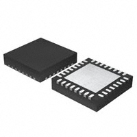
AVAILABLE PACKAGE OPTIONS
(1)
(2)
TA
PACKAGED DEVICE (1) (2)
32-Pin QFN (RHB)
SYMBOL
–40°C to 85°C
TPA6040A4RHB
RHB
The RHB package is available taped and reeled. To order a taped and reeled part, add the suffix R to
the part number (e.g., TPA6040A4RHBR).
For the most current package and ordering information, see the Package Option Addendum at the end
of this document, or see the TI website at www.ti.com.
VDD
REG_OUT
SGND
HP_INL
HP_INR
REG_EN
31
30
29
28
27
26
25
24
1
SPKR_RIN+
2
23
SPKR_EN
SPKR_LIN+
3
22
HP_EN
SPKR_LIN–
4
21
SPGND
SPGND
5
20
ROUT+
LOUT+
6
19
ROUT–
LOUT–
7
18
SPVDD
SPVDD
8
15
17
16
HPVDD
HP_OUTL
GAIN0
32
SPKR_RIN–
HP_OUTR
GAIN1
TPA6040A4RHB
(TOP VIEW)
10
11
12 13
14
C1P
C1N
CPVSS
HPVSS
CPVDD
9
CPGND
Thermal
Pad
BYPASS
TERMINAL FUNCTIONS
TERMINAL
NAME
NO.
I/O/P
DESCRIPTION
SPKR_RIN–
1
I
Right-channel negative differential audio input for speaker amplifier
SPKR_RIN+
2
I
Right-channel positive differential audio input for speaker amplifier
SPKR_LIN+
3
I
Left-channel positive differential audio input for speaker amplifier
SPKR_LIN–
4
I
Left-channel negative differential audio input for speaker amplifier
SPGND
5, 21
P
Speaker power ground
LOUT+
6
O
Left-channel positive audio output
LOUT–
7
O
Left-channel negative audio output
SPVDD
8, 18
P
Supply voltage terminal for speaker amplifier
Charge pump positive supply, connect to HPVDD via star connection
CPVDD
9
P
C1P
10
I/O
CPGND
11
P
C1N
12
I/O
CPVSS
13
P
Charge pump output (negative supply for headphone amplifier), connect to HPVSS
HPVSS
14
P
Headphone amplifier negative supply, connect to CPVSS
HP_OUTR
15
O
Right-channel capacitor-free headphone output
HP_OUTL
16
O
Left-channel capacitor-free headphone output
HPVDD
17
P
Headphone amplifier supply voltage, connect to CPVDD
ROUT–
19
O
Right-channel negative audio output
Charge pump flying capacitor positive terminal
Charge pump ground
Charge pump flying capacitor negative terminal
Submit Documentation Feedback
3
�TPA6040A4
www.ti.com
SLOS519A – APRIL 2007 – REVISED APRIL 2007
TERMINAL FUNCTIONS (continued)
TERMINAL
I/O/P
DESCRIPTION
NAME
NO.
ROUT+
20
O
Right-channel positive audio output
HP_EN
22
I
Headphone channel enable logic input; active high enable. HIGH=ENABLE.
SPKR_EN
23
I
Speaker channel enable logic input; active low enable. LOW=ENABLE.
BYPASS
24
P
Common-mode bias voltage for speaker preamplifiers
REG_EN
25
I
Enable pin (Active HIGH) for turning on/off LDO. HIGH=ENABLE
HP_INR
26
I
Headphone right-channel audio input
HP_INL
27
I
Headphone left-channel audio input
SGND
28
P
Signal ground, connect to CPGND and SPGND
REG_OUT
29
O
Regulated 4.75-V output
VDD
30
P
Positive power supply
GAIN0
31
I
Bit 0, MSB, of gain select bits
GAIN1
32
I
Bit 1, LSB, of gain select bits
Die Pad
P
Solder the thermal pad on the bottom of the QFN package to the GND plane of the PCB. It is required for
mechanical stability and will enhance thermal performance.
Thermal Pad
ABSOLUTE MAXIMUM RATINGS
over operating free-air temperature range (unless otherwise noted) (1)
Supply voltage
VI
Input voltage
HPVDD, VDD, SPVDD, CPVDD
VALUE
UNIT
-0.3 to 6
V
SPKR_LIN+, SPKR_LIN-, SPKR_RIN+, SPKR_RIN-,
HP_EN,GAIN0, GAIN1, SPK_EN, REG_EN
-0.3 to 6.3
HP_INL, HP_INR HP Enabled
-3.5 to 3.5
HP_INL, HP_INR HP not Enabled
-0.3 to 3.5
Continuous total power dissipation
V
See Dissipation Rating Table
TA
Operating free-air temperature range
-40 to 85
°C
TJ
Operating junction temperature range
-40 to 150
°C
Tstg
Storage temperature range
-65 to 150
°C
260
°C
8
kV
CDM
500
V
HBM
2
kV
Lead temperature 1,6 mm (1/16 inch) from case for 10 seconds
(1)
Electrostatic discharge
HBM for HP_OUTL and HP_OUTR
Electrostatic discharge,
all other pins
Stresses beyond those listed under absolute maximum ratings may cause permanent damage to the device. These are stress ratings
only, and functional operations of the device at these or any other conditions beyond those indicated under recommended operating
conditions is not implied. Exposure to absolute-maximum-rated conditions for extended periods may affect device reliability.
DISSIPATION RATINGS
(1)
PACKAGE (1)
TA≤ 25°C
DERATING FACTOR
TA = 70°C
TA = 85°C
RHB
5.06 W
40 mW/°C
4.04 W
3.23 W
The PowerPAD™ must be soldered to a thermal land on the printed-circuit board. Refer to the Texas Instruments document,
PowerPAD™ Thermally Enhanced Package application report (literature number SLMA002) for more information regarding the
PowerPAD™ package.
RECOMMENDED OPERATING CONDITIONS
4
Supply voltage
VDD, SPVDD
Supply voltage
HPVDD, CPVDD
Submit Documentation Feedback
MIN
MAX
4.5
5.5
UNIT
V
3
5.5
V
�TPA6040A4
www.ti.com
SLOS519A – APRIL 2007 – REVISED APRIL 2007
RECOMMENDED OPERATING CONDITIONS (continued)
MIN
VIH
High-level input voltage
SPKR_EN, HP_EN, GAIN0, GAIN1, REG_EN
VIL
Low-level input voltage
SPKR_EN, HP_EN, GAIN0, GAIN1, REG_EN
TA
Operating free-air temperature
MAX
2
UNIT
V
0.8
V
-40
85
°C
TYP
MAX
GENERAL DC ELECTRICAL CHARACTERISTICS
TA = 25°C, VDD = SPVDD = HPVDD = CPVDD = 5 V (unless otherwise noted)
PARAMETER
TEST CONDITIONS
MIN
UNIT
IIH
High-level input current
SPKR_EN, HP_EN, GAIN0, GAIN1,
REG_EN = VDD
0.02
1
µA
IIL
Low-level input current
SPKR_EN, HP_EN, GAIN0, GAIN1,
REG_EN = 0 V
0.02
1
µA
IDD(Speaker)
Supply current, speaker amplifier
ONLY enabled
SPKR_EN = 0 V, HP_EN = REG_EN = 0 V
5
12
mA
IDD(HP)
Supply current, headphone
amplifier ONLY enabled
SPKR_EN = HP_EN = 2 V, REG_EN = 0 V
7.5
14
mA
IDD(REG)
Supply current, regulator ONLY
enabled
SPKR_EN = REG_EN = 2 V, HP_EN = 0 V
0.65
1
mA
IDD(SD)
Supply current, shutdown mode
SPKR_EN = 2 V, HP_EN = REG_EN = 0 V
2.5
5
µA
MIN
TYP
MAX
0.5
10
-60
-74
SPEAKER AMPLIFIER DC CHARACTERISTICS
TA = 25°C, VDD = SPVDD = 5 V, RL = 4 kΩ, Gain = 6 dB (unless otherwise noted)
PARAMETER
TEST CONDITIONS
| VOO |
Output offset voltage (measured differentially)
Inputs AC-coupled to GND, Gain = 6 dB
PSRR
Power supply rejection ratio
VDD = SPVDD = 4.5 V to 5.5 V
UNIT
mV
dB
SPEAKER AMPLIFIER AC CHARACTERISTICS
TA = 25°C, VDD = SPVDD = 5 V, RL = 4 Ω, Gain = 6 dB (unless otherwise noted)
PARAMETER
PO
Output power
TEST CONDITIONS
MIN
1.25
THD+N = 10%, f = 1 kHz, RL = 8 Ω
1.5
THD+N = 1%, f = 1 kHz, RL = 4 Ω
Total harmonic distortion plus noise
Supply ripple rejection ratio
SNR
Signal-to-noise rejection ratio
Maximum output at THD+N


 工商网监
湘ICP备2023018690号
工商网监
湘ICP备2023018690号

