User's Guide
SLVU994 – November 2013
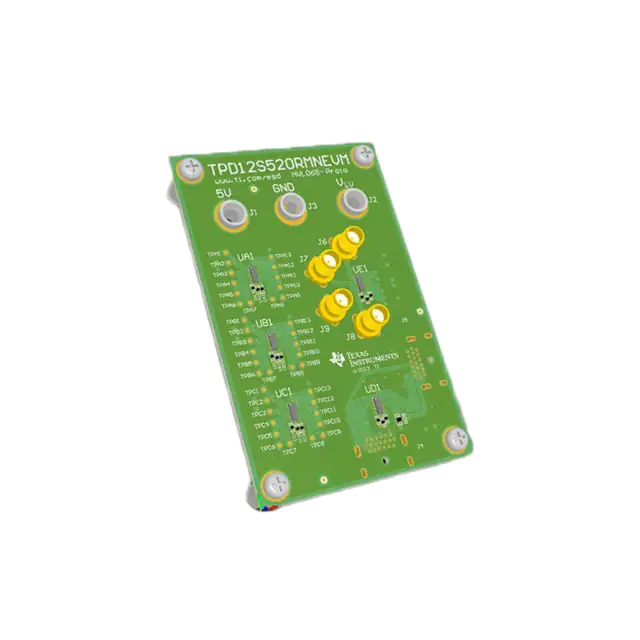
TPD12S520RMN EVM
This user's guide describes the characteristics, operation, and use of the TPD12S520RMNEVM
Evaluation Module (EVM). This EVM includes 5 TPD12S520RMN’s in various configurations for testing.
Three TPD12S520 RMN’s are configured for IEC61000-4-2 compliance testing, one TPD12S520RMN is
configured for throughput on HDMI 1.4a Type A connectors for throughput analysis, and one is configured
to allow 4-port analysis using a vector network analyzer. This user's guide includes setup instructions,
schematic diagrams, a bill of materials, and printed-circuit board layout drawings for the EVM.
1
2
3
4
5
6
Contents
Introduction ..................................................................................................................
Definitions ....................................................................................................................
Board Setup .................................................................................................................
3.1
UA1—UC1 ..........................................................................................................
3.2
UD1 ..................................................................................................................
3.3
UE1 ..................................................................................................................
Board Layout ................................................................................................................
Schematics ...................................................................................................................
Bill of Materials ..............................................................................................................
2
2
3
3
5
5
5
8
9
List of Figures
1
Ideal Contact Discharge Waveform of the Output Current of the ESD Simulator at 4 kV .........................
3
2
1 of 3 TPD12S520RMN for IEC-61000-4-2 Tests ......................................................................
4
3
System Level ESD Test Setup ............................................................................................
4
4
Top Layer ....................................................................................................................
5
5
Layer 2
.......................................................................................................................
.......................................................................................................................
Bottom layer .................................................................................................................
TPD12S520RMNEVM Schematics .......................................................................................
6
6
Layer 3
6
7
8
7
8
List of Tables
1
EVM Configuration ..........................................................................................................
2
IEC61000-4-2 Test Levels .................................................................................................
3
3
Waveform Parameters in Contact Discharge Mode ....................................................................
3
4
Bill of Materials ..............................................................................................................
9
SLVU994 – November 2013
Submit Documentation Feedback
TPD12S520RMN EVM
Copyright © 2013, Texas Instruments Incorporated
2
1
�Introduction
1
www.ti.com
Introduction
Texas Instrument’s TPD12S520RMNEVM evaluation module helps designers evaluate the operation and
performance of the TPD12S520RMNEVM device. TheTPD12S520 is a single-chip electrostatic discharge
(ESD) solution for the high-definition multi-media interface (HDMI) receiver port. The low-speed control
lines offer voltage level-shifting to eliminate the need for an external voltage-level shifter IC. Control-line
ESD clamps add 3.5-pF capacitance to the control lines.
Table 1. EVM Configuration
2
Reference Designator
TI Part Number
Configuration
UA1 – UC1
TPD12S520RMN
IEC61000-4-2 ESD Tests
UD1
TPD12S520RMN
HDMI 1.4 Eye Diagrams
UE1
TPD12S520RMN
S-parameters
Definitions
1. Contact Discharge – a method of testing in which the electrode of the ESD simulator is held in contact
with the device-under-test (DUT).
2
TPD12S520RMN EVM
SLVU994 – November 2013
Submit Documentation Feedback
Copyright © 2013, Texas Instruments Incorporated
�Board Setup
www.ti.com
2. Air Discharge – a method of testing in which the charged electrode of the ESD simulator approaches
the DUT, and a spark to the DUT actuates the discharge.
3. ESD simulator – a device that outputs IEC61000-4-2 compliance ESD waveforms shown in Figure 1
with adjustable ranges shown in Table 2 and Table 3.
IEC61000-4-2 has 4 classes of protection levels. Classes 1 – 4 are shown in Table 2. Stress tests should
be incrementally tested to level 4 as shown in Table 3 until the point of failure. If the DUT does not fail at
8kV, testing can continue in 2 kV increments until failure.
Table 2. IEC61000-4-2 Test Levels
Contact Discharge Class
Test Voltage [± kV]
Air Discharge Class
Test Voltage [± kV]
1
2
1
2
2
4
2
4
3
6
3
8
4
8
4
15
Table 3. Waveform Parameters in Contact Discharge Mode
Stress
Level
Step
Simulator Voltage
[kV]
Ipeak ±15%
[A]
Rise Time ±25%
[nS]
Current at 30ns ±30%
[A]
Current at 60ns ±30%
[A]
1
2
7.5
0.8
4
2
2
4
15
0.8
8
4
3
6
22.5
0.8
12
6
4
8
30
0.8
16
8
Figure 1. Ideal Contact Discharge Waveform of the Output Current of the ESD Simulator at 4 kV
3
Board Setup
This section describes the intended use of the TPD12S520RMNEVM. A generalized outline of the
procedure given in IEC-61000-4-2 is described here. IEC-61000-4-2 should be referred to for a more
specific testing outline.
3.1
UA1—UC1
Three separate and identical test setups for TPD12S520RMN (UA1–UC1) are pinned out to allow
evaluating device performance during ESD events. The devices can be powered up (or not) so that all
operating conditions can be evaluated.
SLVU994 – November 2013
Submit Documentation Feedback
TPD12S520RMN EVM
Copyright © 2013, Texas Instruments Incorporated
3
�Board Setup
www.ti.com
To test powered up: Connect 5V to 5V (J1), 3.3V to VLV
(J2), and connect ground to GND (J3).
To test un-powered: Connect ground to 5V (J1), VLV (J2),
and GND (J3).
Figure 2. 1 of 3 TPD12S520RMN for
IEC-61000-4-2 Tests
3.1.1
Test Method and Set-Up
An example test setup is shown in Figure 3. Details of the testing table and ground planes can be found in
the IEC 61000-4-2 test procedure. Ground the EVM using the banana connector labeled GND (J9).
Discharge the ESD simulator on any of the Test Points TPA1–TPA13. Contact and air-gap discharge are
tested using the same simulator with the same discharge waveform. While the simulator is in direct
contact with the test point during contact, it is not during air-gap.
Figure 3. System Level ESD Test Setup
3.1.2
Evaluation of Test Results
Connect the tested device on the EVM to a curve tracer both before and after ESD testing. After each
incremental level, if the IV curve of the ESD protection diode shifts ±0.1V, or leakage current increases by
a factor of ten, then the device is permanently damaged by ESD.
4
TPD12S520RMN EVM
SLVU994 – November 2013
Submit Documentation Feedback
Copyright © 2013, Texas Instruments Incorporated
�Board Layout
www.ti.com
3.2
UD1
A single TPD12S520RMN (UD1) is configured with two HDMI 1.4a Type A female connectors (J4 and J5)
for capturing Eye Diagrams. Connect 5V to 5V (J1), 3.3V to VLV (J2), and connect ground to GND (J3).
Using either J4 or J5 as input or output attach to an HDMI compliant Eye Diagram test setup and follow
the manufacturer’s instructions for performing signal integrity tests.
3.3
UE1
A single TPD12S520RMN (UE1) is configured with 4 SMA (J1–J4) connectors to allow 4-port analysis with
a vector network analyzer. Connect Port 1 to J6, Port 2 to J7, Port 3 to J8, and Port 4 to J9. Connect 5V
to 5V (J1), 3.3V to VLV (J2), and connect ground to GND (J3). Follow the vector analyzer’s manufacturer’s
instructions to obtain signal integrity parameters. This configuration allows for the following terminology in
4 port analysis:
• S11: Return loss
• S21: Insertion loss
• S31: Near end cross talk
• S41: Far end cross talk
4
Board Layout
Figure 4. Top Layer
SLVU994 – November 2013
Submit Documentation Feedback
TPD12S520RMN EVM
Copyright © 2013, Texas Instruments Incorporated
5
�Board Layout
www.ti.com
Figure 5. Layer 2
Figure 6. Layer 3
6
TPD12S520RMN EVM
SLVU994 – November 2013
Submit Documentation Feedback
Copyright © 2013, Texas Instruments Incorporated
�Board Layout
www.ti.com
Figure 7. Bottom layer
SLVU994 – November 2013
Submit Documentation Feedback
TPD12S520RMN EVM
Copyright © 2013, Texas Instruments Incorporated
7
�Schematics
5
www.ti.com
Schematics
Figure 8. TPD12S520RMNEVM Schematics
8
TPD12S520RMN EVM
SLVU994 – November 2013
Submit Documentation Feedback
Copyright © 2013, Texas Instruments Incorporated
�Bill of Materials
www.ti.com
6
Bill of Materials
Table 4. Bill of Materials
Qty.
Designator
Description
Part Number
Manufacturer
16
CA1, CA2, CA3, CB1,
CB2, CB3, CC1, CC2,
CC3, CD1, CD2, CD3,
CD4, CE1, CE2, CE3
CAP, CERM, 0.1uF, 50V, +/-10%, C0G/NP0, 0402
C1005X7R1H104K
TDK
3
J1, J2, J3
Standard Banana Jack, Un-insulated, 5.5mm
575-4
Keystone
2
J4, J5
Connector, HDMI, 19-Pos Receptacle, SMT
1746679-1
TE Connectivity
4
J6, J7, J8, J9
Connector, TH, SMA
142-0701-201
Emerson Network
Power
25
RA1, RA2, RA7, RA8,
RA9, RB1, RB2, RB7,
RB8, RB9, RC1, RC2,
RC7, RC8, RC9, RD1,
RD2, RD6, RD7, RD8,
RE1, RE2, RE7, RE8,
RE9
RES, 47k ohm, 5%, 0.1W, 0603
CRCW060347K0JNEA
Vishay-Dale
5
RA3, RB3, RC3, RD3,
RE3
RES, 27.4 ohm, 1%, 0.1W, 0603
CRCW060327R4FKEA
Vishay-Dale
5
RA4, RB4, RC4, RD4,
RE4
RES, 1.00k ohm, 1%, 0.1W, 0603
CRCW06031K00FKEA
Vishay-Dale
5
RA5, RB5, RC5, RD5,
RE5
RES, 100k ohm, 5%, 0.1W, 0603
CRCW0603100KJNEA
Vishay-Dale
5
RA6, RB6, RC6, RD9,
RE6
RES, 10k ohm, 5%, 0.1W, 0604
CRCW060310K0JNEA
Vishay-Dale
5
UA1, UB1, UC1, UD1,
UE1
SINGLE-CHIP HDMI RECEIVER PORT
PROTECTION AND INTERFACE DEVICE,
RMN0024A
TPD12S520RMN
Texas
Instruments
SLVU994 – November 2013
Submit Documentation Feedback
TPD12S520RMN EVM
Copyright © 2013, Texas Instruments Incorporated
9
�IMPORTANT NOTICE
Texas Instruments Incorporated and its subsidiaries (TI) reserve the right to make corrections, enhancements, improvements and other
changes to its semiconductor products and services per JESD46, latest issue, and to discontinue any product or service per JESD48, latest
issue. Buyers should obtain the latest relevant information before placing orders and should verify that such information is current and
complete. All semiconductor products (also referred to herein as “components”) are sold subject to TI’s terms and conditions of sale
supplied at the time of order acknowledgment.
TI warrants performance of its components to the specifications applicable at the time of sale, in accordance with the warranty in TI’s terms
and conditions of sale of semiconductor products. Testing and other quality control techniques are used to the extent TI deems necessary
to support this warranty. Except where mandated by applicable law, testing of all parameters of each component is not necessarily
performed.
TI assumes no liability for applications assistance or the design of Buyers’ products. Buyers are responsible for their products and
applications using TI components. To minimize the risks associated with Buyers’ products and applications, Buyers should provide
adequate design and operating safeguards.
TI does not warrant or represent that any license, either express or implied, is granted under any patent right, copyright, mask work right, or
other intellectual property right relating to any combination, machine, or process in which TI components or services are used. Information
published by TI regarding third-party products or services does not constitute a license to use such products or services or a warranty or
endorsement thereof. Use of such information may require a license from a third party under the patents or other intellectual property of the
third party, or a license from TI under the patents or other intellectual property of TI.
Reproduction of significant portions of TI information in TI data books or data sheets is permissible only if reproduction is without alteration
and is accompanied by all associated warranties, conditions, limitations, and notices. TI is not responsible or liable for such altered
documentation. Information of third parties may be subject to additional restrictions.
Resale of TI components or services with statements different from or beyond the parameters stated by TI for that component or service
voids all express and any implied warranties for the associated TI component or service and is an unfair and deceptive business practice.
TI is not responsible or liable for any such statements.
Buyer acknowledges and agrees that it is solely responsible for compliance with all legal, regulatory and safety-related requirements
concerning its products, and any use of TI components in its applications, notwithstanding any applications-related information or support
that may be provided by TI. Buyer represents and agrees that it has all the necessary expertise to create and implement safeguards which
anticipate dangerous consequences of failures, monitor failures and their consequences, lessen the likelihood of failures that might cause
harm and take appropriate remedial actions. Buyer will fully indemnify TI and its representatives against any damages arising out of the use
of any TI components in safety-critical applications.
In some cases, TI components may be promoted specifically to facilitate safety-related applications. With such components, TI’s goal is to
help enable customers to design and create their own end-product solutions that meet applicable functional safety standards and
requirements. Nonetheless, such components are subject to these terms.
No TI components are authorized for use in FDA Class III (or similar life-critical medical equipment) unless authorized officers of the parties
have executed a special agreement specifically governing such use.
Only those TI components which TI has specifically designated as military grade or “enhanced plastic” are designed and intended for use in
military/aerospace applications or environments. Buyer acknowledges and agrees that any military or aerospace use of TI components
which have not been so designated is solely at the Buyer's risk, and that Buyer is solely responsible for compliance with all legal and
regulatory requirements in connection with such use.
TI has specifically designated certain components as meeting ISO/TS16949 requirements, mainly for automotive use. In any case of use of
non-designated products, TI will not be responsible for any failure to meet ISO/TS16949.
Products
Applications
Audio
www.ti.com/audio
Automotive and Transportation
www.ti.com/automotive
Amplifiers
amplifier.ti.com
Communications and Telecom
www.ti.com/communications
Data Converters
dataconverter.ti.com
Computers and Peripherals
www.ti.com/computers
DLP® Products
www.dlp.com
Consumer Electronics
www.ti.com/consumer-apps
DSP
dsp.ti.com
Energy and Lighting
www.ti.com/energy
Clocks and Timers
www.ti.com/clocks
Industrial
www.ti.com/industrial
Interface
interface.ti.com
Medical
www.ti.com/medical
Logic
logic.ti.com
Security
www.ti.com/security
Power Mgmt
power.ti.com
Space, Avionics and Defense
www.ti.com/space-avionics-defense
Microcontrollers
microcontroller.ti.com
Video and Imaging
www.ti.com/video
RFID
www.ti-rfid.com
OMAP Applications Processors
www.ti.com/omap
TI E2E Community
e2e.ti.com
Wireless Connectivity
www.ti.com/wirelessconnectivity
Mailing Address: Texas Instruments, Post Office Box 655303, Dallas, Texas 75265
Copyright © 2013, Texas Instruments Incorporated
�