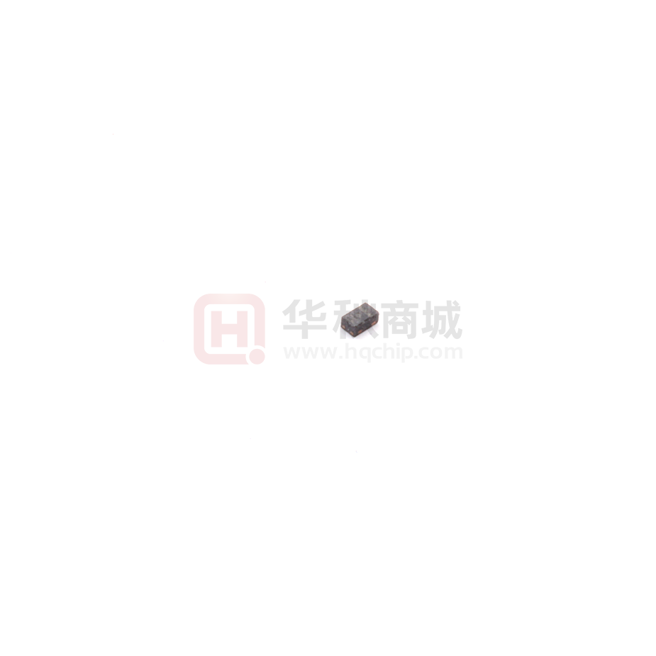
TPD1E10B06-Q1
ZHCSFE0B – AUGUST 2016 – REVISED FEBRUARY 2022
TPD1E10B06-Q1 采用 0402 和 SOD-523 封装的汽车类 12pF、±5.5V、±30kV 单通
道 ESD 保护二极管
1 特性
3 说明
• 符合 AEC-Q101 标准
• IEC 61000-4-2 级 4 ESD 保护
– ±30kV 接触放电
– ±30kV 气隙放电
• ISO 10605(330pF,330Ω)ESD 保护
– ±8kV 接触放电 (DPY)
– ±15kV 气隙放电 (DPY)
– ±25kV 接触放电 (DYA)
– ±25kV 气隙放电 (DYA)
• IEC 61000-4-5 浪涌保护
– 6A (8µs/20µs)
• I/O 电容 12pF(典型值)
• RDYN:0.38Ω(典型值)
• 直流击穿电压:±6V(最小值)
• 超低泄漏电流 100nA(最大值)
• 10V 钳位电压(IPP = 1A 时的典型值)
• 工业温度范围:–40°C 至 +125°C
• 节省空间的 0402 外形尺寸
• 业界通用引线式 SOD-523 封装
(1.6mm × 0.8mm × 0.65mm)
TPD1E10B06-Q1 器件是一款双向 TVS ESD 保护二极
管,提供适合空间受限应用的小型 0402 封装,以及业
界通用的引线式 SOD-523 封装,以支持自动光学检测
(AOI)。TPD1E10B06-Q1 的额定 ESD 冲击耗散值高
于 IEC 61000-4-2 4 级国际标准规定的最高水平,原因
是其 ESD 电压可轻松升至 5000V,超出足以损坏众多
集成电路的电压值,但在极端条件下,这些电压将显著
升高。例如,在湿度较低的环境下,电压可超过
20000V。
低动态电阻和低钳位电压可确保提供系统级瞬变事件保
护,从而为暴露于 ESD 事件下的设计提供充分保护。
该器件还具有 12pF IO 电容,因此非常适用于音频线
路、按钮、存储器接口或 GPIO。
该 器 件 还 具 有 未 经 过 汽 车 认 证 的 型 号 :
TPD1E10B06。
器件信息(1)
器件型号
TPD1E10B06-Q1
2 应用
(1)
• 终端设备:
– 音响主机
– 高端音响
– 外部放大器
– 车身控制模块
– 网关
– 远程信息处理系统
– 摄像头模块
• 接口:
– 音频线路
– 按钮
– 存储器接口
– GPIO
L Audio IN
封装
封装尺寸(标称值)
X1SON (2)
0.6mm x 1.00mm
SOD-523 (2)
0.80 mm × 1.2 mm
如需了解所有可用封装,请参阅数据表末尾的可订购产品附
录。
Audio amplifier
class AB
(ESD Sensitive)
L Audio
L
GND
R Audio IN
Speaker
connector
(source of ESD)
1
1
R Audio
Audio amplifier
class AB
(ESD Sensitive)
R
GND
2
GND
2
典型应用原理图
本文档旨在为方便起见,提供有关 TI 产品中文版本的信息,以确认产品的概要。有关适用的官方英文版本的最新信息,请访问
www.ti.com,其内容始终优先。TI 不保证翻译的准确性和有效性。在实际设计之前,请务必参考最新版本的英文版本。
English Data Sheet: SLVSDN7
�TPD1E10B06-Q1
www.ti.com.cn
ZHCSFE0B – AUGUST 2016 – REVISED FEBRUARY 2022
Table of Contents
1 特性................................................................................... 1
2 应用................................................................................... 1
3 说明................................................................................... 1
4 Revision History.............................................................. 2
5 Pin Configuration and Functions...................................3
6 Specifications.................................................................. 4
6.1 Absolute Maximum Ratings........................................ 4
ESD Ratings - AEC Specification..................................... 4
6.2 ESD Ratings—IEC Specification................................ 4
6.3 ESD Ratings—ISO Specification................................ 4
6.4 Recommended Operating Conditions.........................4
6.5 Thermal Information....................................................4
6.6 Electrical Characteristics.............................................5
6.7 Typical Characteristics................................................ 6
7 Detailed Description........................................................8
7.1 Overview..................................................................... 8
7.2 Functional Block Diagram........................................... 8
7.3 Feature Description.....................................................8
7.4 Device Functional Modes............................................9
8 Application and Implementation.................................. 10
8.1 Application Information............................................. 10
8.2 Typical Application.................................................... 10
9 Power Supply Recommendations................................12
10 Layout...........................................................................12
10.1 Layout Guidelines................................................... 12
10.2 Layout Example...................................................... 12
11 Device and Documentation Support..........................13
11.1 Documentation Support.......................................... 13
11.2 接收文档更新通知................................................... 13
11.3 支持资源..................................................................13
11.4 Trademarks............................................................. 13
11.5 Electrostatic Discharge Caution.............................. 13
11.6 术语表..................................................................... 13
12 Mechanical, Packaging, and Orderable
Information.................................................................... 13
4 Revision History
Changes from Revision A (August 2016) to Revision B (February 2022)
•
•
•
•
•
•
•
•
•
•
•
•
Page
更新了整个文档中的表格、图和交叉参考的编号格式......................................................................................... 1
更新了特性 部分,以添加 DPY (X1SON) 和 DYA (SOD-523) 封装特性.............................................................1
更新了说明 部分..................................................................................................................................................1
在器件信息 表中添加了 DYA 封装详情............................................................................................................... 1
从器件信息 表中删除了 TPD1E10B06 器件........................................................................................................1
Added the DYA package to the Pin Configuration and Functions section.......................................................... 3
Updated the Overview section............................................................................................................................8
Updated the Functional Block Diagram ............................................................................................................. 8
Updated the Feature Description section........................................................................................................... 8
Updated the ISO 10605 ESD Protection section................................................................................................ 8
Updated the Typical Application Schematic figure............................................................................................10
Updated the Related Documentation section................................................................................................... 13
Changes from Revision * (August 2016) to Revision A (August 2016)
Page
• 将器件状态从产品预发布 更改为量产数据 ......................................................................................................... 1
2
Submit Document Feedback
Copyright © 2022 Texas Instruments Incorporated
Product Folder Links: TPD1E10B06-Q1
�TPD1E10B06-Q1
www.ti.com.cn
ZHCSFE0B – AUGUST 2016 – REVISED FEBRUARY 2022
5 Pin Configuration and Functions
1
2
图 5-1. DPY Package, 2-Pin X1SON (Top View)
ID Area
1
2
图 5-2. DYA Package, 2-Pin SOD-523 (Top View)
表 5-1. Pin Functions
PIN
NO.
NAME
1
IO
2
IO
(1)
TYPE(1)
I/O
DESCRIPTION
ESD Protected I/O. Connect other pin to ground
I = input, O = output
Submit Document Feedback
Copyright © 2022 Texas Instruments Incorporated
Product Folder Links: TPD1E10B06-Q1
3
�TPD1E10B06-Q1
www.ti.com.cn
ZHCSFE0B – AUGUST 2016 – REVISED FEBRUARY 2022
6 Specifications
6.1 Absolute Maximum Ratings
over operating free-air temperature range (unless otherwise noted)(1)
MIN
Peak pulse
UNIT
IEC 61000-4-5 power (tp - 8/20 µs) at 25°C
90
W
IEC 61000-4-5 current (tp - 8/20 µs) at 25°C
6
A
-40
125
°C
–65
155
°C
TA
Operating free-air temperature
Tstg
Storage temperature
(1)
MAX
Stresses beyond those listed under Absolute Maximum Rating may cause permanent damage to the device. These are stress ratings
only, which do not imply functional operation of the device at these or any other conditions beyond those indicated under
Recommended Operating Condition. Exposure to absolute-maximum-rated conditions for extended periods may affect device
reliability.
ESD Ratings - AEC Specification
V(ESD)
Electrostatic discharge - DPY
V(ESD)
Electrostatic discharge - DYA
VALUE
UNIT
Human body model (HBM), per AEC Q100-002
±2500
V
Charged device model (CDM), per AEC
Q100-011
±1000
V
Human body model (HBM), per AEC Q101-001
±2500
V
Charged device model (CDM), per AEC
Q101-005
±1000
V
VALUE
UNIT
IEC 61000-4-2 Contact Discharge, all pins
±30000
IEC 61000-4-2 Air-gap Discharge, all pins
±30000
6.2 ESD Ratings—IEC Specification
V(ESD)
Electrostatic discharge
V
6.3 ESD Ratings—ISO Specification
VALUE
UNIT
V(ESD)
Electrostatic discharge
ISO 10605, 330-pF, 330-Ω (DPY)
Air-gap discharge
± 15000
V
V(ESD)
Electrostatic discharge
ISO 10605, 330-pF, 330-Ω (DPY)
Contact discharge
± 8000
V
V(ESD)
Electrostatic discharge
ISO 10605, 330-pF, 330-Ω (DYA)
Air-gap discharge
± 25000
V
V(ESD)
Electrostatic discharge
ISO 10605, 330-pF, 330-Ω (DYA)
Contact discharge
± 25000
V
6.4 Recommended Operating Conditions
over operating free-air temperature range (unless otherwise noted)
MIN
Operating
voltage
Pin 1 to 2 or Pin 2 to 1
TA
Operating free-air temperature
NOM
MAX
UNIT
–5.5
5.5
V
-40
125
°C
6.5 Thermal Information
THERMAL METRIC(1)
4
DPY (X1SON)
DYA (SOD523)
2 PINS
2 PINS
UNIT
RθJA
Junction-to-ambient thermal resistance
615.5
730.8
°C/W
RθJC(top)
Junction-to-case (top) thermal resistance
404.8
413.4
°C/W
Submit Document Feedback
Copyright © 2022 Texas Instruments Incorporated
Product Folder Links: TPD1E10B06-Q1
�TPD1E10B06-Q1
www.ti.com.cn
ZHCSFE0B – AUGUST 2016 – REVISED FEBRUARY 2022
6.5 Thermal Information (continued)
THERMAL METRIC(1)
DPY (X1SON)
DYA (SOD523)
2 PINS
2 PINS
UNIT
RθJB
Junction-to-board thermal resistance
493.3
497.7
°C/W
ΨJT
Junction-to-top characterization parameter
127.7
129.7
°C/W
ΨJB
Junction-to-board characterization parameter
493.3
491.8
°C/W
RθJC(bot)
Junction-to-case (bottom) thermal resistance
162
-
°C/W
(1)
For more information about traditional and new thermal metrics, see the Semiconductor and IC Package Thermal Metrics application
report.
6.6 Electrical Characteristics
over operating free-air temperature range (unless otherwise noted)
PARAMETER
TEST CONDITION
MIN
TYP
MAX
UNIT
VRWM
Reverse stand-off voltage
Pin 1 to 2 or Pin 2 to 1
5.5
V
ILEAK
Leakage current
Pin 1 = 5 V, Pin 2 = 0 V
100
nA
VClamp1,2
Clamp voltage with surge strike on pin 1,
pin 2 grounded.
IPP = 1 A, tp = 8/20 µs(2)
10
V
VClamp1,2
Clamp voltage with surge strike on pin 1,
pin 2 grounded.
IPP =5 A, tp = 8/20 µs(2)
14
V
VClamp2,1
Clamp voltage with surge strike on pin 2,
pin 1 grounded.
IPP = 1 A, tp = 8/20 µs(2)
8.5
V
VClamp2,1
Clamp voltage with surge strike on pin 2,
pin 1 grounded.
IPP =5 A, tp = 8/20 µs(2)
14
V
RDYN
Dynamic resistance
CIO
I/O capacitance
VIO = 2.5 V; ƒ = 1 MHz
VBR1,2
Break-down voltage, pin 1 to pin 2
IIO = 1 mA
6
V
VBR2,1
Break-down voltage, pin 2 to pin 1
IIO = 1 mA
6
V
(1)
(2)
Pin 1 to Pin 2(1)
0.32
Pin 2 to Pin 1(1)
0.38
12
Ω
pF
Extraction of RDYN using least squares fit of TLP characteristics between IPP = 10 A and IPP = 20 A.
Nonrepetitive current pulse 8 to 20 µs exponentially decaying waveform according to IEC 61000-4-5
Submit Document Feedback
Copyright © 2022 Texas Instruments Incorporated
Product Folder Links: TPD1E10B06-Q1
5
�TPD1E10B06-Q1
www.ti.com.cn
ZHCSFE0B – AUGUST 2016 – REVISED FEBRUARY 2022
6.7 Typical Characteristics
图 6-2. IEC 61000-4-2 Clamp Voltage –8-kV Contact ESD
图 6-3. Transmission Line Pulse (TLP) Waveform Pin 1 to Pin 2
图 6-4. Transmission Line Pulse (TLP) Waveform Pin 2 to Pin 1
Current (A)
10
9
150
Current
Power 135
8
120
7
105
6
90
5
75
4
60
3
45
2
30
1
15
0
-10
图 6-5. IV Curve
6
0
10
20
30
40
Time (Ps)
50
60
Power (W)
图 6-1. IEC 61000-4-2 Clamp Voltage +8-kV Contact ESD
0
70
D001
图 6-6. Positive Surge Waveform (8/20 µs)
Submit Document Feedback
Copyright © 2022 Texas Instruments Incorporated
Product Folder Links: TPD1E10B06-Q1
�TPD1E10B06-Q1
www.ti.com.cn
ZHCSFE0B – AUGUST 2016 – REVISED FEBRUARY 2022
6.7 Typical Characteristics (continued)
110
Current
100
Power
90
10
Current (A)
9
8
80
7
70
6
60
5
50
4
40
3
30
2
20
1
10
0
-10
0
10
20
30
40
Time (Ps)
50
60
Power (W)
11
0
70
D002
图 6-7. Negative Surge Waveform (8/20 µs)
图 6-8. Pin Capacitance Across VBIAS
图 6-9. Insertion Loss
Submit Document Feedback
Copyright © 2022 Texas Instruments Incorporated
Product Folder Links: TPD1E10B06-Q1
7
�TPD1E10B06-Q1
www.ti.com.cn
ZHCSFE0B – AUGUST 2016 – REVISED FEBRUARY 2022
7 Detailed Description
7.1 Overview
The TPD1E10B06-Q1 is a single-channel ESD TVS diode in a 0402 package convenient for space constrained
applications and an industry standard SOD-523 package. This TVS protection product offers ±30-kV IEC air-gap,
±30-kV contact ESD protection, and has an ESD clamp circuit with a back-to-back TVS diode for bipolar or
bidirectional signal support. The 12-pF line capacitance of this ESD protection diode is suitable for a wide range
of applications supporting data rates up to 400 Mbps.
Typical application of this ESD protection product is the circuit protection for audio lines, push buttons, memory
interfaces, and general-purpose I/O ports. This ESD clamp is a good fit for the protection of the end equipments
such as head units, premium audio, external amplifiers, and many other automotive applications.
7.2 Functional Block Diagram
1
2
7.3 Feature Description
The TPD1E10B06-Q1 is a bidirectional TVS with high ESD protection level. This device protects the circuit from
ESD strikes up to ±30-kV contact and ±30-kV air-gap specified in the IEC 61000-4-2 Level 4 international
standard. The device can also handle up to 6-A surge current (IEC 61000-4-5 8/20 µs). The I/O capacitance of
12 pF supports a data rate up to 400 Mbps. This clamping device has a small dynamic resistance, which makes
the clamping voltage low when the device is actively protecting other circuits. For example, the clamping voltage
is only 10 V when the device is taking 1-A transient current. The breakdown is bidirectional so that this protection
device is a good fit for GPIO and especially audio lines which carry bidirectional signals. Low leakage allows the
diode to conserve power when working below the VRWM. The industrial temperature range of –40°C to +125°C
makes this ESD device work at extensive temperatures in most environments. The space-saving 0402 package
can fit into many flexible spaces, whereas in the leaded SOD-523 package is good for applications requiring
automatic optical inspection (AOI).
7.3.1 AEC-Q101 Qualified
This device is qualified to AEC-Q101 standards and is qualified to operate from –40°C to +125°C.
7.3.2 IEC 61000-4-2 ESD Protection
The I/O pins can withstand ESD events up to ±30-kV contact and ±30-kV air according to the IEC 61000-4-2
standard. An ESD-surge clamp diverts the current to ground.
7.3.3 ISO 10605 ESD Protection
The I/O pins can withstand ESD events at least ±25-kV contact and ±25-kV air in the leaded SOD-523 package
according to the ISO 10605 (330 pF, 330 Ω) standard. An ESD-surge clamp diverts the current to ground.
7.3.4 IEC 61000-4-5 Surge Protection
The IO pins can withstand surge events up to 6 A (8/20 µs waveform). An ESD-surge clamp diverts this current
to ground.
7.3.5 IO Capacitance
The capacitance between the I/O pins is 12 pF. This capacitance support data rates up to 400 Mbps.
8
Submit Document Feedback
Copyright © 2022 Texas Instruments Incorporated
Product Folder Links: TPD1E10B06-Q1
�TPD1E10B06-Q1
www.ti.com.cn
ZHCSFE0B – AUGUST 2016 – REVISED FEBRUARY 2022
7.3.6 Dynamic Resistance
The IO pins feature an ESD clamp that has a low RDYN of 0.32 Ω (Pin 1 to Pin 2) and 0.38 Ω (Pin 2 to Pin 1)
which prevents system damage during ESD events.
7.3.7 DC Breakdown Voltage
The DC breakdown voltage between the IO pins is a minimum of 6 V. This ensures that sensitive equipment is
protected from surges above the reverse standoff voltage of 5.5 V.
7.3.8 Ultra Low Leakage Current
The IO pins feature an ultra-low leakage current of 100 nA (maximum) with a bias of 5 V.
7.3.9 Clamping Voltage
The IO pins feature an ESD clamp that is capable of clamping the voltage to 10 V (IPP = 1 A) and 14V (IPP = 5
A).
7.3.10 Industrial Temperature Range
This device features an industrial operating range of –40°C to +125°C
7.3.11 Space-Saving Footprint
This device features a space-saving, industry standard 0402 footprint.
7.4 Device Functional Modes
The TPD1E10B06-Q1 is a passive clamp that has low leakage during normal operation when the voltage
between pin 1 and pin 2 is below VRWM and activates when the voltage between pin 1 and pin 2 goes above
VBR. During IEC ESD events, transient voltages as high as ±30 kV can be clamped between the two pins. When
the voltages on the protected lines fall below the trigger voltage, the device reverts back to the low leakage
passive state.
Submit Document Feedback
Copyright © 2022 Texas Instruments Incorporated
Product Folder Links: TPD1E10B06-Q1
9
�TPD1E10B06-Q1
www.ti.com.cn
ZHCSFE0B – AUGUST 2016 – REVISED FEBRUARY 2022
8 Application and Implementation
备注
以下应用部分中的信息不属于 TI 器件规格的范围,TI 不担保其准确性和完整性。TI 的客 户应负责确定
器件是否适用于其应用。客户应验证并测试其设计,以确保系统功能。
8.1 Application Information
When a system contains a human interface connector, the system becomes vulnerable to large system-level
ESD strikes that standard ICs cannot survive. TVS ESD protection diodes are typically used to suppress ESD at
these connectors. The TPD1E10B06-Q1 is a single-channel ESD protection device containing back-to-back TVS
diodes, which is typically used to provide a path to ground for dissipating ESD events on bidirectional signal lines
between a human interface connector and a system. As the current from ESD passes through the device, only a
small voltage drop is present across the diode structure. This is the voltage presented to the protected IC. The
low RDYN of the triggered TVS holds this voltage, VCLAMP, to a tolerable level to the protected IC.
8.2 Typical Application
L Audio IN
Audio amplifier
class AB
(ESD Sensitive)
L Audio
L
GND
R Audio IN
Speaker
connector
(source of ESD)
1
R Audio
Audio amplifier
class AB
(ESD Sensitive)
1
R
GND
2
GND
2
图 8-1. Typical Application Schematic
8.2.1 Design Requirements
For this design example, the two TPD1E10B06-Q1s are used to protect left and right audio channels. For this
audio application, the system parameters shown in 表 8-1 are known.
表 8-1. Design Parameters
DESIGN PARAMETER
VALUE
Audio amplifier class
AB
Audio signal voltage range
–3 V to 3 V
Audio frequency content
20 Hz to 20 kHz
Required IEC 61000-4-2 ESD protection
±20-kV contact, ±25-kV air-gap
8.2.2 Detailed Design Procedure
To begin the design process, some parameters must be decided upon; the designer must make sure:
• Voltage range on the protected line must not exceed the reverse standoff voltage of the TVS diode(s) (VRWM)
• Operating frequency is supported by the I/O capacitance CIO of the TVS diode
• IEC 61000-4-2 protection requirement is covered by the IEC performance of the TVS diode
10
Submit Document Feedback
Copyright © 2022 Texas Instruments Incorporated
Product Folder Links: TPD1E10B06-Q1
�TPD1E10B06-Q1
www.ti.com.cn
ZHCSFE0B – AUGUST 2016 – REVISED FEBRUARY 2022
For this application, the audio signal voltage range is –3 V to 3 V. The VRWM for the TVS is –5.5 V to 5.5 V;
therefore, the bidirectional TVS does not break down during normal operation, and therefore normal operation of
the audio signal is not effected because of the signal voltage range. In this application, a bidirectional TVS like
TPD1E10B06-Q1 is required.
Next, consider the frequency content of this audio signal. In this application with the class AB amplifier, the
frequency content is from 20 Hz to 20 kHz; ensure that the TVS I/O capacitance does not distort this signal by
filtering it. With the TPD1E10B06-Q1 typical capacitance of 12 pF, which leads to a typical 3-dB bandwidth of
400 MHz, this diode has sufficient bandwidth to pass the audio signal without distorting it.
Finally, the human interface in this application requires above standard Level 4 IEC 61000-4-2 system-level ESD
protection (±20-kV Contact, ±25-kV Air-Gap). A standard TVS cannot survive this level of IEC ESD stress.
However, the TPD1E10B06-Q1 can survive at least ±30-kV Contact/ ±30-kV Air-Gap. Therefore, the device can
provide sufficient ESD protection for the interface, even though the requirements are stringent. For any TVS
diode to provide the full range of ESD protection capabilities, as well as to minimize the noise and EMI
disturbances the board will see during ESD events, a system designer must use proper board layout of their TVS
ESD protection diodes. See 节 10 for instructions on properly laying out TPD1E10B06-Q1.
8.2.3 Application Curves
图 8-2. IEC 61000-4-2 Clamp Voltage +8-kV Contact
ESD
图 8-3. IEC 61000-4-2 Clamp Voltage –8-kV
Contact ESD
Submit Document Feedback
Copyright © 2022 Texas Instruments Incorporated
Product Folder Links: TPD1E10B06-Q1
11
�TPD1E10B06-Q1
www.ti.com.cn
ZHCSFE0B – AUGUST 2016 – REVISED FEBRUARY 2022
9 Power Supply Recommendations
This device is a passive TVS diode-based ESD protection device, therefore there is no requirement to power it.
Take care to make sure that the maximum voltage specifications for each pin are not violated.
10 Layout
10.1 Layout Guidelines
• The optimum placement is as close to the connector as possible.
– EMI during an ESD event can couple from the trace being struck to other nearby unprotected traces,
resulting in early system failures.
– The PCB designer must minimize the possibility of EMI coupling by keeping any unprotected traces away
from the protected traces which are between the TVS and the connector.
• Route the protected traces as straight as possible.
• Eliminate any sharp corners on the protected traces between the TVS and the connector by using rounded
corners with the largest radii possible.
– Electric fields tend to build up on corners, increasing EMI coupling.
• If pin 1 or pin 2 is connected to ground, use a thick and short trace for this return path.
10.2 Layout Example
To connector
To protected IC
Place pin 1 on the signal line
Minimum
distance
from
connector
(source of
ESD)
Thick and short return path to GND
图 10-1. Layout Recommendation
12
Submit Document Feedback
Copyright © 2022 Texas Instruments Incorporated
Product Folder Links: TPD1E10B06-Q1
�TPD1E10B06-Q1
www.ti.com.cn
ZHCSFE0B – AUGUST 2016 – REVISED FEBRUARY 2022
11 Device and Documentation Support
11.1 Documentation Support
11.1.1 Related Documentation
For related documentation, see the following:
• Texas Instruments, ESD Layout Guide user's guide
• Texas Instruments, ESD Protection Diodes EVM user's guide
• Texas Instruments, Generic ESD Evaluation Module user's guide
• Texas Instruments, Reading and Understanding an ESD Protection data sheet
• Texas Instruments, TPD1E10B06-Q1 Evaluation Module user's guide
11.2 接收文档更新通知
要接收文档更新通知,请导航至 ti.com 上的器件产品文件夹。点击订阅更新 进行注册,即可每周接收产品信息更
改摘要。有关更改的详细信息,请查看任何已修订文档中包含的修订历史记录。
11.3 支持资源
TI E2E™ 支持论坛是工程师的重要参考资料,可直接从专家获得快速、经过验证的解答和设计帮助。搜索现有解
答或提出自己的问题可获得所需的快速设计帮助。
链接的内容由各个贡献者“按原样”提供。这些内容并不构成 TI 技术规范,并且不一定反映 TI 的观点;请参阅
TI 的《使用条款》。
11.4 Trademarks
TI E2E™ is a trademark of Texas Instruments.
所有商标均为其各自所有者的财产。
11.5 Electrostatic Discharge Caution
This integrated circuit can be damaged by ESD. Texas Instruments recommends that all integrated circuits be handled
with appropriate precautions. Failure to observe proper handling and installation procedures can cause damage.
ESD damage can range from subtle performance degradation to complete device failure. Precision integrated circuits may
be more susceptible to damage because very small parametric changes could cause the device not to meet its published
specifications.
11.6 术语表
TI 术语表
本术语表列出并解释了术语、首字母缩略词和定义。
12 Mechanical, Packaging, and Orderable Information
The following pages include mechanical, packaging, and orderable information. This information is the most
current data available for the designated devices. This data is subject to change without notice and revision of
this document. For browser-based versions of this data sheet, refer to the left-hand navigation.
Submit Document Feedback
Copyright © 2022 Texas Instruments Incorporated
Product Folder Links: TPD1E10B06-Q1
13
�PACKAGE OPTION ADDENDUM
www.ti.com
3-Mar-2022
PACKAGING INFORMATION
Orderable Device
Status
(1)
Package Type Package Pins Package
Drawing
Qty
Eco Plan
(2)
Lead finish/
Ball material
MSL Peak Temp
Op Temp (°C)
Device Marking
(3)
(4/5)
(6)
TPD1E10B06DYARQ1
ACTIVE
SOT-5X3
DYA
2
3000
RoHS & Green
SN
Level-3-260C-168 HR
-40 to 125
1KG
TPD1E10B06QDPYRQ1
ACTIVE
X1SON
DPY
2
10000
RoHS & Green
NIPDAU
Level-1-260C-UNLIM
-40 to 125
4M
(1)
The marketing status values are defined as follows:
ACTIVE: Product device recommended for new designs.
LIFEBUY: TI has announced that the device will be discontinued, and a lifetime-buy period is in effect.
NRND: Not recommended for new designs. Device is in production to support existing customers, but TI does not recommend using this part in a new design.
PREVIEW: Device has been announced but is not in production. Samples may or may not be available.
OBSOLETE: TI has discontinued the production of the device.
(2)
RoHS: TI defines "RoHS" to mean semiconductor products that are compliant with the current EU RoHS requirements for all 10 RoHS substances, including the requirement that RoHS substance
do not exceed 0.1% by weight in homogeneous materials. Where designed to be soldered at high temperatures, "RoHS" products are suitable for use in specified lead-free processes. TI may
reference these types of products as "Pb-Free".
RoHS Exempt: TI defines "RoHS Exempt" to mean products that contain lead but are compliant with EU RoHS pursuant to a specific EU RoHS exemption.
Green: TI defines "Green" to mean the content of Chlorine (Cl) and Bromine (Br) based flame retardants meet JS709B low halogen requirements of


 工商网监
湘ICP备2023018690号
工商网监
湘ICP备2023018690号
