Product
Folder
Order
Now
Support &
Community
Tools &
Software
Technical
Documents
TPD4E001-Q1
SLLSEG0F – MARCH 2013 – REVISED SEPTEMBER 2017
TPD4E001-Q1 4-Channel ESD Protection Array With 1.5-pF I/O Capacitance
1 Features
3 Description
•
The TPD4E001-Q1 device is a low-capacitance TVS
diode array designed for ESD protection in sensitive
electronics connected to communication lines. Each
channel consists of a pair of transient-voltagesuppression diodes that steer ESD pulses to VCC or
GND. The TPD4E001-Q1 protects against ESD
events up to ±8-kV contact discharge and ±15-kV airgap discharge, as specified in IEC 61000-4-2
international standard. This device has a low
capacitance of 1.5-pF per channel making it ideal for
use in high-speed data interfaces. The low leakage
current (10 nA maximum) ensures minimum power
consumption for the system and high accuracy for
analog interfaces.
1
•
•
•
•
•
AEC-Q100 Qualified With the Following Results:
– Device Temperature Grade 1: –40°C to 125°C
Ambient Operating Temperature Range
– Device HBM ESD Classification Level 3B
– HBM Level 15 kV
– Device CDM ESD Classification Level C5
IEC 61000-4-2 Level 4 ESD Protection
– ±8-kV Contact Discharge
– ±15-kV Air-Gap Discharge
IEC 61000-4-5 Surge Protection
– 5.5 A (8/20 µs)
Low 1.5-pF Input Capacitance
Low 10-nA Maximum Leakage Current
0.9-V to 5.5-V Supply Voltage Range
Additionally, this device is ideal for protecting
automotive head units, automotive rear seat
entertainment, and automotive rear camera systems
that use USB 2.0, Ethernet, or precision analog
interfaces.
2 Applications
•
•
Device Information(1)
End Equipment
– Automotive Head Unit
– Automotive Rear Seat Entertainment
– Automotive Rear Camera Systems
Interfaces
– USB 2.0
– Ethernet
– Precision Analog Interfaces
PART NUMBER
TPD4E001-Q1
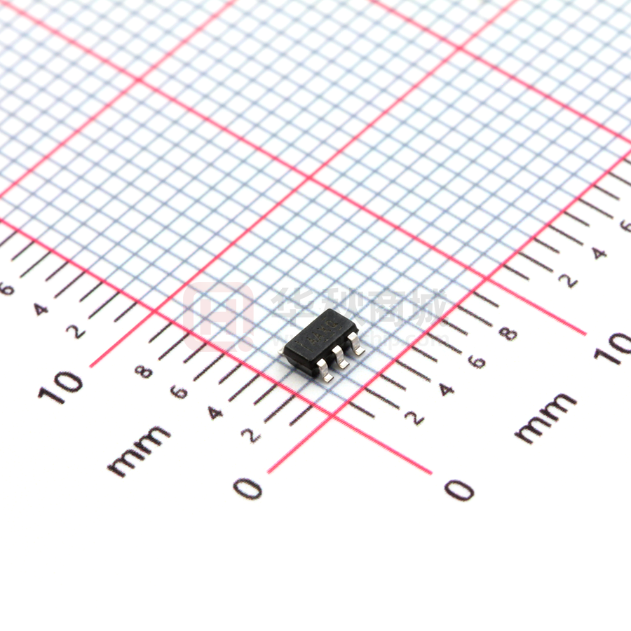
PACKAGE
SOT-23 (6)
BODY SIZE (NOM)
2.90 mm × 1.60 mm
(1) For all available packages, see the orderable addendum at
the end of the datasheet.
Typical Schematic
VBUS
0.1 µF
VCC
D+
D–
RT
GND
IO4
IO1
USB
Controller
D1
IO3
IO2
VBUS
D+
GND
D–
GND
1
An IMPORTANT NOTICE at the end of this data sheet addresses availability, warranty, changes, use in safety-critical applications,
intellectual property matters and other important disclaimers. PRODUCTION DATA.
�TPD4E001-Q1
SLLSEG0F – MARCH 2013 – REVISED SEPTEMBER 2017
www.ti.com
Table of Contents
1
2
3
4
5
6
7
Features ..................................................................
Applications ...........................................................
Description .............................................................
Revision History.....................................................
Pin Configuration and Functions .........................
Specifications.........................................................
1
1
1
2
3
4
6.1
6.2
6.3
6.4
6.5
6.6
6.7
6.8
4
4
4
4
5
5
5
6
Absolute Maximum Ratings .....................................
ESD Ratings—AEC Specification .............................
ESD Ratings—IEC Specification ..............................
ESD Ratings—ISO Specification ..............................
Recommended Operating Conditions.......................
Thermal Information ..................................................
Electrical Characteristics...........................................
Typical Characteristics ..............................................
Detailed Description .............................................. 7
7.1 Overview ................................................................... 7
7.2 Functional Block Diagram ......................................... 7
7.3 Feature Description .................................................. 7
7.4 Device Functional Modes.......................................... 8
8
Application and Implementation .......................... 9
8.1 Application Information.............................................. 9
8.2 Typical Application ................................................... 9
9 Power Supply Recommendations...................... 11
10 Layout................................................................... 12
10.1 Layout Guidelines ................................................. 12
10.2 Layout Example .................................................... 12
11 Device and Documentation Support ................. 13
11.1
11.2
11.3
11.4
11.5
11.6
Documentation Support ........................................
Receiving Notification of Documentation Updates
Community Resources..........................................
Trademarks ...........................................................
Electrostatic Discharge Caution ............................
Glossary ................................................................
13
13
13
13
13
13
12 Mechanical, Packaging, and Orderable
Information ........................................................... 13
4 Revision History
NOTE: Page numbers for previous revisions may differ from page numbers in the current version.
Changes from Revision E (June 2017) to Revision F
•
Added ISO Specification......................................................................................................................................................... 4
Changes from Revision D (March 2015) to Revision E
•
Page
Page
Updated Typical Application Schematic ................................................................................................................................. 9
Changes from Revision C (June 2013) to Revision D
Page
•
Added Pin Configuration and Functions section, ESD Ratings table, Feature Description section, Device Functional
Modes, Application and Implementation section, Power Supply Recommendations section, Layout section, Device
and Documentation Support section, and Mechanical, Packaging, and Orderable Information section ............................... 1
•
Changed Device CDM ESD Classification Level from C4B to C5 ........................................................................................ 1
Changes from Revision B (February 2012) to Revision C
•
Page
Changed maximum ICC supply current in Electrical Characteristics....................................................................................... 5
Changes from Revision A (April 2013) to Revision B
Page
•
Revised text in DESCRIPTION section .................................................................................................................................. 1
•
Revised Figure 2 graph .......................................................................................................................................................... 5
•
Revised APPLICATION INFORMATION schematic .............................................................................................................. 9
2
Submit Documentation Feedback
Copyright © 2013–2017, Texas Instruments Incorporated
Product Folder Links: TPD4E001-Q1
�TPD4E001-Q1
www.ti.com
SLLSEG0F – MARCH 2013 – REVISED SEPTEMBER 2017
5 Pin Configuration and Functions
DBV Package
6-Pin SOT-23
Top View
IO1
1
6
IO4
GND
2
5
VCC
IO2
3
4
IO3
Pin Functions
PIN
NAME
NO.
GND
2
IO1
1
IO2
3
IO3
4
IO4
6
VCC
5
TYPE
GND
I/O
I
DESCRIPTION
Ground
ESD-protected channel
Power-supply input. Bypass VCC to GND with a 0.1-μF ceramic capacitor
Submit Documentation Feedback
Copyright © 2013–2017, Texas Instruments Incorporated
Product Folder Links: TPD4E001-Q1
3
�TPD4E001-Q1
SLLSEG0F – MARCH 2013 – REVISED SEPTEMBER 2017
www.ti.com
6 Specifications
6.1 Absolute Maximum Ratings
over operating free-air temperature range (unless otherwise noted)
(1)
MIN
MAX
UNIT
VCC
Supply voltage
–0.3
7
V
VIO
I/O voltage tolerance
–0.3
VCC + 0.3
V
IPP
Peak pulse current (Tp = 8/20 µs) (2)
5.5
A
PPP
Peak pulse power (Tp = 8/20 µs) (2)
100
W
TA
Free air operating temperature
125
°C
TJ
Junction temperature
150
°C
Tstg
Storage temperature
150
°C
(1)
(2)
–40
–65
SStresses beyond those listed under Absolute Maximum Ratings may cause permanent damage to the device. These are stress ratings
only, which do not imply functional operation of the device at these or any other conditions beyond those indicated under Recommended
Operating Conditions. Exposure to absolute-maximum-rated conditions for extended periods may affect device reliability.
Non-repetitive current pulse 8/20 µs exponentially decaying waveform according to IEC 61000-4-5.
6.2 ESD Ratings—AEC Specification
VALUE
V(ESD)
(1)
Electrostatic
discharge
Human-body model (HBM), per AEC Q100-002
(1)
UNIT
±15000
Charged-device model (CDM), per AEC Q100-011
V
±750
AEC Q100-002 indicates that HBM stressing shall be in accordance with the ANSI/ESDA/JEDEC JS-001 specification.
6.3 ESD Ratings—IEC Specification
VALUE
V(ESD)
Electrostatic discharge
IEC 61000-4-2 contact discharge
±8000
IEC 61000-4-2 air-gap discharge
±15000
UNIT
V
6.4 ESD Ratings—ISO Specification
VALUE
V(ESD)
4
Electrostatic discharge
ISO 10605 (330 pF, 330 Ω) contact discharge
±8000
ISO 10605 (330 pF, 330 Ω) air-gap discharge
±15000
Submit Documentation Feedback
UNIT
V
Copyright © 2013–2017, Texas Instruments Incorporated
Product Folder Links: TPD4E001-Q1
�TPD4E001-Q1
www.ti.com
SLLSEG0F – MARCH 2013 – REVISED SEPTEMBER 2017
6.5 Recommended Operating Conditions
over operating free-air temperature range (unless otherwise noted)
MIN
MAX
UNIT
TA
Free air operating temperature
–40
125
°C
VCC pin
Operating voltage
0.9
5.5
V
IO1, IO2, IO3,
IO4 pins
Operating voltage
0
VCC
V
6.6 Thermal Information
TPD4E001-Q1
THERMAL METRIC
(1)
DBV (SOT-23)
UNIT
6 PINS
RθJA
Junction-to-ambient thermal resistance
202.1
°C/W
RθJC(top)
Junction-to-case (top) thermal resistance
146.2
°C/W
RθJB
Junction-to-board thermal resistance
47.1
°C/W
ψJT
Junction-to-top characterization parameter
37.6
°C/W
ψJB
Junction-to-board characterization parameter
46.7
°C/W
(1)
For more information about traditional and new thermal metrics, see the Semiconductor and IC Package Thermal Metrics application
report.
6.7 Electrical Characteristics
VCC = 5 V ± 10%, over operating free-air temperature range (unless otherwise noted)
PARAMETER
TEST CONDITIONS
ICC
Supply current
VF
Diode forward voltage
IF = 10 mA
VBR
Breakdown voltage
IBR = 10 mA
MIN
TYP (1)
1
0.65
MAX
UNIT
200
nA
0.95
V
11
V
(2)
VCLAMP
Clamping voltage
Surge strike on IO pin, GND pin
grounded, VCC = 5.5 V, IPP = 5.5 A
VRWM
Reverse standoff voltage
IO pin to GND pin
IIO
Channel leakage current
VIO = GND to VCC
CIO
Channel input capacitance
VCC = 5 V, bias of VCC/2, f = 10 MHz
(1)
(2)
Positive transients
16
V
5.5
V
±10
nA
1.5
pF
Typical values are at VCC = 5 V and TA = 25°C.
Non-repetitive current pulse 8/20 µs exponentially decaying waveform according to IEC 61000-4-5.
Submit Documentation Feedback
Copyright © 2013–2017, Texas Instruments Incorporated
Product Folder Links: TPD4E001-Q1
5
�TPD4E001-Q1
SLLSEG0F – MARCH 2013 – REVISED SEPTEMBER 2017
www.ti.com
6.8 Typical Characteristics
2.20
100
VIO = 5.5 V
VCC = 5.5 V
90
IO Leakage Current (pA)
IO Capacitance (pF)
2.00
1.80
1.60
1.40
1.20
80
70
60
50
40
30
20
10
1.00
1.00
2.00
2.50
3.00
4.00
0
5.00
±55
±35
±15
IO Voltage (V)
IPP (A)
6
25
45
65
85
105
Temperature (ºC)
Figure 1. IO Capacitance vs IO Voltage (VCC = 5 V)
6.0
5.5
5.0
4.5
4.0
3.5
3.0
2.5
2.0
1.5
1.0
0.5
0.0
5
125
C001
Figure 2. IO Leakage Current vs Temperature
100
90
80
70
Current (A)
60
50
40
PPP (W)
0.00
30
Power (W)
20
10
0
5
10
15
20
25
30
35
40
45
Time (μs)
Figure 3. Peak Pulse Waveform, VCC = 5.5 V
Submit Documentation Feedback
0
50
Copyright © 2013–2017, Texas Instruments Incorporated
Product Folder Links: TPD4E001-Q1
�TPD4E001-Q1
www.ti.com
SLLSEG0F – MARCH 2013 – REVISED SEPTEMBER 2017
7 Detailed Description
7.1 Overview
The TPD4E001-Q1 device is a low-capacitance, TVS diode array designed for ESD protection in sensitive
electronics connected to communication lines. Each channel consists of a pair of transient voltage suppression
diodes that steer ESD pulses to VCC or GND. The TPD4E001-Q1 device protects against ESD events up to ±8kV contact discharge and ±15-kV air-gap discharge, as specified in IEC 61000-4-2 international standard. This
device has a low capacitance of 1.5-pF per channel making it ideal for use in high-speed data interfaces. The
low-leakage current (10 nA maximum) ensures minimum power consumption for the system and high accuracy
for analog interfaces.
7.2 Functional Block Diagram
VCC
IO1
IO3
IO2
IO4
GND
7.3 Feature Description
7.3.1 AEC-Q100 Qualified
This device is qualified according to the AEC-Q100 standard. The device temperature rating is Grade 1 (–40°C
to +125°C). The HBM Classification Level passed is 3B (> 8 kV). The CDM Classification Level passed is C5 (all
pins 750 V to


 工商网监
湘ICP备2023018690号
工商网监
湘ICP备2023018690号