User's Guide
SLVUAA4 – September 2014
Using the TPS22945EVM-082 Single Channel Current
Limited Load Switch IC
The TPS22945EVM-082 evaluation module (EVM) allows the user to connect power to and control the 5pin DCK package load switch. The features of the current limiting switch can be easily evaluated using the
EVM connections. Table 1 lists a short description of the TPS22945 load switch performance
specifications; for additional details on load switch performance, application notes, and the datasheet see
ti.com/loadswitch.
1
2
3
4
5
6
7
Contents
Introduction ...................................................................................................................
1.1
Description ...........................................................................................................
1.2
Features ..............................................................................................................
Electrical Performance ......................................................................................................
Schematic .....................................................................................................................
Layout .........................................................................................................................
4.1
Setup .................................................................................................................
Operation .....................................................................................................................
Test Configurations ..........................................................................................................
6.1
On-Resistance (RON) Test Setup ..................................................................................
6.2
Timing Test Setup ..................................................................................................
6.3
Some Examples of TPS22945 Fault Detection Conditions ...................................................
Bill of Materials (BOM) ......................................................................................................
2
2
2
2
2
3
4
5
5
5
6
7
8
List of Figures
...........................................................................................
.......................................................................................
TPS22945EVM-082 Top Layout ...........................................................................................
TPS22945EVM-082 Bottom Layout .......................................................................................
RON Setup .....................................................................................................................
Typical Timing Setup ........................................................................................................
TPS22945 Over Current Shutdown (VIN = 3.3V) .........................................................................
TPS22945 Operating in Constant Current Mode with Auto Restart (VIN = 3.3V) ....................................
1
TPS22945EVM-082 Schematic
2
2
TPS22945EVM-082 Top Assembly
3
3
4
5
6
7
8
3
4
5
6
7
7
List of Tables
1
TPS22945 Current Limit, Blanking Time, Enable, and Auto Restart Characteristics ............................... 2
2
TPS22945EVM-082 Bill of Materials ...................................................................................... 8
SLVUAA4 – September 2014
Submit Documentation Feedback
Using the TPS22945EVM-082 Single Channel Current Limited Load Switch
IC
Copyright © 2014, Texas Instruments Incorporated
1
�Introduction
1
www.ti.com
Introduction
Table 1. TPS22945 Current Limit, Blanking Time, Enable, and Auto Restart Characteristics
1.1
EVM
Device
Current Limit Minimum
Current Limit Blanking
Time
Auto Restart
Time
Enable (ON Pin)
HVL082
TPS22945
100 mA
10 ms
80 ms
Active High
Description
The TPS22945EVM is a two sided PCB containing the TPS22945 load switch device. The VIN and VOUT
connections to the device and the PCB layout routing provide a low resistance pathway into and out of the
device under test. Test point connections allow the EVM User to control the device with user defined test
conditions and make accurate RON and timing measurements.
1.2
Features
•
•
•
•
2
VIN input voltage range: 1.62 V to 5.5 V.
EVM allows access to the VIN, VOUT, GND, ON and OC pin of the TPS22945 Load Switch Device.
On board CIN and COUT capacitors.
VIN Sense and VOUT Sense test points provide an accurate measurement point of contact to the
device.
Electrical Performance
Refer to the datasheet for detailed electrical characteristics of the TPS22945 (SLVS832).
3
Schematic
VIN
200mA Max Output Current
1.62v - 5.5v
U1
J1
5
2
1
VIN
4
C1
1µF
VIN
J2
VOUT
OC
ON
GND
1
1
2
3
TPS22945DCK
VIN Sense
GND
1
2
R2
JP3
JP2
TP3
VOUT
C2
0.1uF
2
510
1
2
JP4
TP4
1
2
VOUT Sense
GND
GND
GND
VIN
JP1
J3
GND
HI
TP1
3
2
1
2
1
ON
R1
10k
OC
J4
TP2
1
2
GND
LO
GND
GND
GND
Figure 1. TPS22945EVM-082 Schematic
2
Using the TPS22945EVM-082 Single Channel Current Limited Load Switch
IC
Copyright © 2014, Texas Instruments Incorporated
SLVUAA4 – September 2014
Submit Documentation Feedback
�Layout
www.ti.com
4
Layout
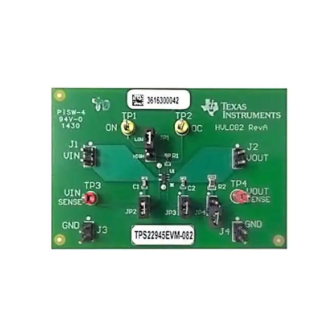
Figure 2. TPS22945EVM-082 Top Assembly
Figure 3. TPS22945EVM-082 Top Layout
SLVUAA4 – September 2014
Submit Documentation Feedback
Using the TPS22945EVM-082 Single Channel Current Limited Load Switch
IC
Copyright © 2014, Texas Instruments Incorporated
3
�Layout
www.ti.com
Figure 4. TPS22945EVM-082 Bottom Layout
4.1
Setup
This section describes the jumpers and connectors on the EVM as well as how to properly connect, set
up, and use the EVM.
4.1.1
J1 – VIN Connection
This is the connection for the positive lead from the input source
4.1.2
J2 – VOUT Connection
This is the connection point for the output of the device.
4.1.3
JP1 – ON
This is the enable input for the device. A shorting jumper must be installed on JP1 in either the High or
Low position. The TPS22945 is active High. ON must not be left floating. An external enable source can
be applied to the EVM by removing the shunt and connecting a signal to TP1. Refer to the datasheet for
proper ON and OFF voltage level settings. A switching signal may also be used and connected at this
point.
4.1.4
TP3 - VIN Sense, TP4 - VOUT Sense
These two connections are used when very accurate measurements of the input or output are required.
RON measurements should be made using these sense connections when measuring the voltage drop
from VIN to VOUT to calculate the resistance.
4
Using the TPS22945EVM-082 Single Channel Current Limited Load Switch
IC
Copyright © 2014, Texas Instruments Incorporated
SLVUAA4 – September 2014
Submit Documentation Feedback
�Operation
www.ti.com
4.1.5
JP2 - Input Capacitor
During normal operation a shorting jumper is placed on JP2 this connects C1 capacitor from the input of
the device to ground. Refer to the Applications Section of the datasheet for additional information on
selecting the input capacitor.
4.1.6
JP3 - Output Capacitor
During normal operation a shorting jumper is placed on JP3 this connects C2 capacitor from the output of
the device to ground. Refer to the Applications Section of the datasheet for additional information on
selecting the output capacitor.
4.1.7
J3 – J4– GND
These are connections to GND.
5
Operation
Connect the positive input of the VIN power supply to VIN at J1. Connect the negative lead of the power
supply to GND at J3. The input voltage range of the TPS22945EVM-082 is 1.62 V to 5.5 V.
External output loads can be applied to the switch by using J2 VOUT and J4 GND. Configure JP1 as
required. JP1 must be installed for proper operation. When the ON pin is asserted high, the output of the
TPS22945 will be enabled.
6
Test Configurations
6.1
On-Resistance (RON) Test Setup
Figure 5 shows a typical setup for measuring On-Resistance. The voltage drop across the switch is
measured using the sense connections then divided by the current into the load yielding the RON
resistance.
Figure 5. RON Setup
SLVUAA4 – September 2014
Submit Documentation Feedback
Using the TPS22945EVM-082 Single Channel Current Limited Load Switch
IC
Copyright © 2014, Texas Instruments Incorporated
5
�Test Configurations
6.2
www.ti.com
Timing Test Setup
Figure 6 shows a test setup for measuring some of the typical timing features of the TPS22945 load
switch. The OC output pin will switch to a low state when an overload condition or other fault conditions
are encountered by the device. Connecting the switch as shown below will allow the user to capture these
fault conditions with an oscilloscope.
Figure 6. Typical Timing Setup
6
Using the TPS22945EVM-082 Single Channel Current Limited Load Switch
IC
Copyright © 2014, Texas Instruments Incorporated
SLVUAA4 – September 2014
Submit Documentation Feedback
�Test Configurations
www.ti.com
6.3
Some Examples of TPS22945 Fault Detection Conditions
Figure 7. TPS22945 Over Current Shutdown (VIN = 3.3V)
Figure 8. TPS22945 Operating in Constant Current Mode with Auto Restart (VIN = 3.3V)
SLVUAA4 – September 2014
Submit Documentation Feedback
Using the TPS22945EVM-082 Single Channel Current Limited Load Switch
IC
Copyright © 2014, Texas Instruments Incorporated
7
�Bill of Materials (BOM)
7
www.ti.com
Bill of Materials (BOM)
Table 2. TPS22945EVM-082 Bill of Materials
Designator
Qty
Value
Description
Package Reference
Part Number
Manufacturer
HVL082
Any
0603
GRM188R71E105KA12D
Murata
CAP, CERM, 0.1µF, 100V, ±10%, X7R, 0603
0603
GRM188R72A104KA35D
Murata
3
Fiducial mark. There is nothing to buy or mount.
Fiducial
N/A
N/A
J1, J2, J3, J4
4
Header, 100mil, 2x1, Gold, TH
Header, 2x1, 100mil
5-146261-1
TE Connectivity
JP1
1
Header, 100mil, 3x1, Tin plated, TH
Header, 3 PIN, 100mil, Tin
PEC03SAAN
Sullins Connector Solutions
JP2, JP3, JP4
3
Header, 100mil, 2x1, Tin plated, TH
Header, 2 PIN, 100mil, Tin
PEC02SAAN
Sullins Connector Solutions
LBL1
1
Thermal Transfer Printable Labels,
0.650" W x 0.200" H - 10,000 per roll
PCB Label
0.650"H x 0.200"W
THT-14-423-10
Brady
R1
1
10k
RES, 10kΩ, 5%, 0.1W, 0603
0603
CRCW060310K0JNEA
Vishay-Dale
R2
1
510
RES, 510 Ω, 5%, 0.125W, 0805
0805
ERJ-6GEYJ511V
Panasonic
TP1, TP2
2
Yellow
Test Point, Multipurpose, Yellow, TH
Yellow Multipurpose
Testpoint
5014
Keystone
TP3, TP4
2
Red
Test Point, Multipurpose, Red, TH
Red Multipurpose Testpoint
5010
Keystone
U1
1
Low-input-voltage current-limited load switches with shut
off and auto-restart feature, DCK0005A
DCK0005A
TPS22945DCK
Texas Instruments
PCB1
1
Printed Circuit Board
C1
1
1µF
CAP, CERM, 1µF, 25V, ±10%, X7R, 0603
C2
1
0.1µF
FID1, FID2, FID3
NOTE: Unless otherwise noted in the Alternate PartNumber and/or Alternate Manufacturer columns, all parts may be substituted with equivalents.
8
Using the TPS22945EVM-082 Single Channel Current Limited Load Switch IC
Copyright © 2014, Texas Instruments Incorporated
SLVUAA4 – September 2014
Submit Documentation Feedback
�IMPORTANT NOTICE
Texas Instruments Incorporated and its subsidiaries (TI) reserve the right to make corrections, enhancements, improvements and other
changes to its semiconductor products and services per JESD46, latest issue, and to discontinue any product or service per JESD48, latest
issue. Buyers should obtain the latest relevant information before placing orders and should verify that such information is current and
complete. All semiconductor products (also referred to herein as “components”) are sold subject to TI’s terms and conditions of sale
supplied at the time of order acknowledgment.
TI warrants performance of its components to the specifications applicable at the time of sale, in accordance with the warranty in TI’s terms
and conditions of sale of semiconductor products. Testing and other quality control techniques are used to the extent TI deems necessary
to support this warranty. Except where mandated by applicable law, testing of all parameters of each component is not necessarily
performed.
TI assumes no liability for applications assistance or the design of Buyers’ products. Buyers are responsible for their products and
applications using TI components. To minimize the risks associated with Buyers’ products and applications, Buyers should provide
adequate design and operating safeguards.
TI does not warrant or represent that any license, either express or implied, is granted under any patent right, copyright, mask work right, or
other intellectual property right relating to any combination, machine, or process in which TI components or services are used. Information
published by TI regarding third-party products or services does not constitute a license to use such products or services or a warranty or
endorsement thereof. Use of such information may require a license from a third party under the patents or other intellectual property of the
third party, or a license from TI under the patents or other intellectual property of TI.
Reproduction of significant portions of TI information in TI data books or data sheets is permissible only if reproduction is without alteration
and is accompanied by all associated warranties, conditions, limitations, and notices. TI is not responsible or liable for such altered
documentation. Information of third parties may be subject to additional restrictions.
Resale of TI components or services with statements different from or beyond the parameters stated by TI for that component or service
voids all express and any implied warranties for the associated TI component or service and is an unfair and deceptive business practice.
TI is not responsible or liable for any such statements.
Buyer acknowledges and agrees that it is solely responsible for compliance with all legal, regulatory and safety-related requirements
concerning its products, and any use of TI components in its applications, notwithstanding any applications-related information or support
that may be provided by TI. Buyer represents and agrees that it has all the necessary expertise to create and implement safeguards which
anticipate dangerous consequences of failures, monitor failures and their consequences, lessen the likelihood of failures that might cause
harm and take appropriate remedial actions. Buyer will fully indemnify TI and its representatives against any damages arising out of the use
of any TI components in safety-critical applications.
In some cases, TI components may be promoted specifically to facilitate safety-related applications. With such components, TI’s goal is to
help enable customers to design and create their own end-product solutions that meet applicable functional safety standards and
requirements. Nonetheless, such components are subject to these terms.
No TI components are authorized for use in FDA Class III (or similar life-critical medical equipment) unless authorized officers of the parties
have executed a special agreement specifically governing such use.
Only those TI components which TI has specifically designated as military grade or “enhanced plastic” are designed and intended for use in
military/aerospace applications or environments. Buyer acknowledges and agrees that any military or aerospace use of TI components
which have not been so designated is solely at the Buyer's risk, and that Buyer is solely responsible for compliance with all legal and
regulatory requirements in connection with such use.
TI has specifically designated certain components as meeting ISO/TS16949 requirements, mainly for automotive use. In any case of use of
non-designated products, TI will not be responsible for any failure to meet ISO/TS16949.
Products
Applications
Audio
www.ti.com/audio
Automotive and Transportation
www.ti.com/automotive
Amplifiers
amplifier.ti.com
Communications and Telecom
www.ti.com/communications
Data Converters
dataconverter.ti.com
Computers and Peripherals
www.ti.com/computers
DLP® Products
www.dlp.com
Consumer Electronics
www.ti.com/consumer-apps
DSP
dsp.ti.com
Energy and Lighting
www.ti.com/energy
Clocks and Timers
www.ti.com/clocks
Industrial
www.ti.com/industrial
Interface
interface.ti.com
Medical
www.ti.com/medical
Logic
logic.ti.com
Security
www.ti.com/security
Power Mgmt
power.ti.com
Space, Avionics and Defense
www.ti.com/space-avionics-defense
Microcontrollers
microcontroller.ti.com
Video and Imaging
www.ti.com/video
RFID
www.ti-rfid.com
OMAP Applications Processors
www.ti.com/omap
TI E2E Community
e2e.ti.com
Wireless Connectivity
www.ti.com/wirelessconnectivity
Mailing Address: Texas Instruments, Post Office Box 655303, Dallas, Texas 75265
Copyright © 2014, Texas Instruments Incorporated
�


 工商网监
湘ICP备2023018690号
工商网监
湘ICP备2023018690号

