User's Guide
SLVUAK6A – October 2015 – Revised September 2016
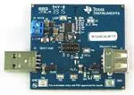
TPS2549Q1EVM-729 Evaluation Module
This User’s Guide describes the evaluation module (EVM) for the TPS2549-Q1 (TPS2549Q1EVM-729).
The TPS2549-Q1 is a USB charging port controller with an integrated power switch and USB 2.0 highspeed data line (DP/DM) switches.
1
2
3
4
5
6
Contents
Introduction ................................................................................................................... 1
Description .................................................................................................................... 2
Schematic ..................................................................................................................... 3
General Configuration and Description ................................................................................... 4
EVM Assembly Drawings and Layout Guidelines ....................................................................... 6
Bill of Materials ............................................................................................................. 13
List of Figures
1
TPS2549Q1EVM-729 Schematic .......................................................................................... 3
2
Typical TPS549Q1EVM-729 Test Setup
3
4
5
6
7
8
................................................................................. 5
Top Side Placement ......................................................................................................... 6
Top Side Routing ............................................................................................................ 7
Layer Two Routing .......................................................................................................... 8
Layer Three Routing ........................................................................................................ 9
Bottom Side Routing ....................................................................................................... 10
Bottom Side Placement ................................................................................................... 11
List of Tables
1
1
Connector Functionality ..................................................................................................... 4
2
Test Points .................................................................................................................... 4
3
Jumpers ....................................................................................................................... 4
4
TPS2549Q1EVM-729 Bill of Materials
..................................................................................
13
Introduction
The TPS2549Q1EVM-729 allows reference circuit evaluation of the TI TPS2549-Q1 automotive USB
charging port controller with integrated power switch and cable compensation. The TPS2549Q1EVM-729
provides the electrical signatures on DP_IN and DM_IN to support all current charging schemes. The
TPS2549Q1EVM-729 incorporates USB cable voltage drop compensation by linearly sensing the port
current and automatically adjusting the output voltage of the LM53603AQ to keep the cable end device
voltage within the normal operating range.
SLVUAK6A – October 2015 – Revised September 2016
Submit Documentation Feedback
TPS2549Q1EVM-729 Evaluation Module
Copyright © 2015–2016, Texas Instruments Incorporated
1
�Introduction
1.1
www.ti.com
Features
The TPS2549-Q1 features include:
• Built-in IEC 61000-4-2 protection on DP_IN and DM_IN pins
• Linear USB cable voltage-droop compensation
• Fully AEC Q100 qualified
• Built-in short to VBUS protection and notification on DP_IN and DM_IN pins
• LM53603AQ high performance 2.1-MHz automotive qualified DC/DC converter
1.2
Applications
The TPS2549-Q1 can be used in the following applications:
• Automotive infotainment system
• Automotive USB charging box
2
Description
The TPS2549Q1EVM-729 enables full evaluation of the TPS2549-Q1 device, refer to the schematic in
Figure 1. An automotive voltage range input is applied at the J3 connector. The input stage consists of an
input switch (Q1), protection (D2), and an input filter (L1, C1, C2, C3, C5). The voltage at the 5VDC node
is regulated by the LM53603AQ buck regulator (U1) and associated circuitry. This provides a nominal 5-V,
3-A output for the TPS2549-Q1 (U2).
The TPS2549-Q1 internal power switch connects the 5VDC node to VBUS at the downstream facing USB
connector, J1. When the internal power switch is ON, the D5 LED (green) will illuminate. USB 2.0 data
can be passed through the TPS2549Q1EVM-729 from J2 to J1 when the TPS2549-Q1 is configured for
either SDP or CDP mode using the J6 header. TPS2549-Q1 status and fault conditions can be detected
using the D4 (blue) and D3 (red) LEDs, respectively.
TPS2549-Q1 provides system-level ESD protection in accordance with IEC 61000-4-2 up to ±8-kV contact
and ±15-kV air discharge at the DP_IN and DM_IN signals going to J1. These pins will also provide
detection of shorts to VBUS by triggering the FAULT logic and illuminating D3.
The TPS2549-Q1 provides USB cable voltage-droop compensation at the load through the use of the CS
pin. Sinking current into the CS pin mirrors the current through the TPS2549-Q1 power switch at a rate of
75 µA/A. The CS pin current is summed with the LM53603AQ regulator feedback current through R8
causing the regulator output voltage to change with USB downstream load current. The voltage at the
5VDC node increases linearly as load current increases. This compensation will keep the load end voltage
close to 5 VDC. The default compensation resistor values (R8 and R10) target a USB cable resistance of
200 mΩ. Three additional cable resistance examples are provided in the following list.
• For 300-mΩ CC: R8 = 5.11 kΩ, R10 = 17.8 kΩ
• For 400-mΩ CC: R8 = 6.49 kΩ, R10 = 16.5 kΩ
• For 500-mΩ CC: R8 = 7.68 kΩ, R10 = 15.4 kΩ
Refer to the TPS2549-Q1 datasheet (SLUSCE3) for more information.
NOTE: The values shown for R8 and R10 take into account the effects of the TPS2549Q1 power
switch and J1 receptacle/plug resistances (approximately 0.1 ohms, total). The effects of R5
are also included. Designs which do not need to account for these losses can exclude these
from the equations.
2
TPS2549Q1EVM-729 Evaluation Module
SLVUAK6A – October 2015 – Revised September 2016
Submit Documentation Feedback
Copyright © 2015–2016, Texas Instruments Incorporated
�Schematic
www.ti.com
3
Schematic
Figure 1 illustrates the EVM schematic.
1
2
3
4
5
6
A
A
1,2,5,6
HVS
INPUT POWER
7V-18V, 1.5A
VIN
12
13
VIN
VIN
CBOOT
3
11
EN
SW
SW
1
2
FB
9
BIAS
5
1uH
R2
1.00M
D1
(40V Transient)
C1
10µF
15V
D2
C2
10µF
C3
0.1µF
R3
C5
10µF
J3
5VDC
U1
L1
Q1
HVIN
100k
8
R7
0
DNP
39V
3.32
RESET
4
VCC
7
FPWM
6
SYNC
VCC
R6
100k
14
B
C4
R4
0.47µF
SW
R23
5VP
L3
2.2uH
0
R8
3.83k
VFB
R1
BIAS
C10
0.022µF
0
AGND
PGND
PGND
PAD
NC
200mΩ
CSPORT
TP8
10
15
16
17
R5
49.9
C9
DNP220uF
C12
2.2µF
C6
22µF
C7
22µF
TP9
C8
22µF
LOOP
B
LM53603AQPWPRQ1
C11
2.2µF
R9
0
R10
19.1k
FSW = 2.1MHz
200mΩ
VFB
5VDC
GND
R11
5.62k
R12
10.0k
R14
10.0k
5016
D3
Red
D4
Blue
TP3
TP4
TP2
D-
C
D+
GND
5V @ 2.4A
TP5
5VBI
1
5
VBUS
J5
J2
J1
U2
2
DM_OUT
3
1
DP_OUT
Sx
9
Fx
13
CS
4
EN
5
4
C17
10µF
R16
6
CSPort
TP6
0
R17
100k
R18
R19
R20
100k
100k
100k
6
7
8
IN
OUT
STATUS
ILIM_LO
ILIM_HI
FAULT
DP_IN
DM_IN
CS
EN
DP_OUT
DM_OUT
CLT1
CLT2
CLT3
GND
PAD
5VBO
12
15
16
10
11
3
2
ILIM_LO
ILIM_HI
C16
0.1µF
2
DM_IN
3
DP_IN
DP_IN
DM_IN
R13
2.00k
4
DP_OUT
DM_OUT
C
VBUS
DD+
GND
14
17
R21
19.1k
GND
C18
10µF
VBUS 1
6
5
J4
TP1
R22
80.6k
C13
0.1µF
C14
47µF
C15
47µF
D5
Green
TP7
TPS2549Q1RTE
J6
CTL1
CTL2
CTL3
1
3
5
7
GND
2
4
6
8
D
D
Texas Instruments and/or its licensors do not warrant the accuracy or c mpleteness of this specification or any information contained therein. Texas Instruments and/or its licensors do not
warrant that this design will meet the specifications, will be suitable for your application or fit for any particular purpose, or will operate in an implementation. Texas Instruments and/or its
licensors do not warrant that the design is production worthy. You shou d completely validate and test your design implementation to confirm the system functionality for your application.
1
2
3
4
Orderable: TPS2549Q1EVM-729
TID #:
N/A
Rev: A
Number: PWR729
SVN Rev: Version control disabled
Drawn By:
Engineer: Milo Zhu
5
Mod. Date: 9/21/2015
Designed for: Public Release
Project Title: Auto USB Charging Port Controller
Sheet Title:
Sheet: 2 of 2
Assembly Variant: 001
File: PWR729A_SH2.SchDoc
Size: B
Contact: http://www.ti.com/support
http://www.ti.com
© Te xas Instruments 2015
6
Figure 1. TPS2549Q1EVM-729 Schematic
SLVUAK6A – October 2015 – Revised September 2016
Submit Documentation Feedback
TPS2549Q1EVM-729 Evaluation Module
Copyright © 2015–2016, Texas Instruments Incorporated
3
�General Configuration and Description
www.ti.com
4
General Configuration and Description
4.1
Physical Access
Table 1 lists the TPS2549Q1EVM-729 connector functionality, Table 2 describes the test point availability,
and Table 3 describes the jumper functionality.
Table 1. Connector Functionality
Connector
Label
J1
Description
DOWNSTREAM Downstream facing USB 2.0 connector. Connect to the USB 2.0 slave for data pass-through
from J2. USB output power is provided to the slave when the J5 shunt is installed.
J2
UPSTREAM
J3
HVIN
Automotive input voltage range connector. Connect to a 7 V–18 V, 1.5-A voltage source
according to the polarity marked on the EVM.
D3 (RED)
FAULT
D4 (BLUE)
STATUS
D5 (GREEN)
Upstream facing USB 2.0 connector. Connect to the USB 2.0 host for data pass-through to
J1. USB input power can also be provided by the host when the J4 shunt is installed.
TPS2549-Q1 FAULT output is triggered
TPS2549-Q1 STATUS output is triggered
ON
TPS2549-Q1 output powered
Table 2. Test Points
Test
Point
Color
Label
Description
TP1
SM-L
GND
Back side GND test point
TP2
SM-S
5VDC
TPS2549-Q1 power switch input from DC-DC converter
TP3
SM-S
STATx
TPS2549-Q1 STATUS pin output
TP4
SM-S
FLTx
TPS2549-Q1 FAULT pin output
TP5
SM-S
5VBO
TPS2549-Q1 power switch output
TP6
SM-L
GND
Top side GND test point near J2
TP7
SM-L
GND
Top side GND test point near J1
TP8
SM-S
CS
Loop injection point, use with TP9
TP9
SM-S
LOOP
Loop injection point, use with TP8
Table 3. Jumpers
4
Jumper
Label
Description
J4
5VDC
USB host furnished input voltage. Install to power TPS2549-Q1 with a USB host.
J5
5VBO
Install to connect TPS2549-Q1 power switch output to J1 VBUS
J6
J6
TPS2549-Q1 mode select jumper block. Install shunt at EN (1-2) to disable TPS2549-Q1. C1, C2, C3
positions select the charging mode for TPS2549-Q1. Refer to the datasheet for more information.
TPS2549Q1EVM-729 Evaluation Module
SLVUAK6A – October 2015 – Revised September 2016
Submit Documentation Feedback
Copyright © 2015–2016, Texas Instruments Incorporated
�General Configuration and Description
www.ti.com
4.2
Test Setup
Figure 2 shows a typical test setup for TPS2549Q1EVM-729. Connect J3 to the 14-V power supply. The
TPS2549-Q1 output load can be applied either between TP5 and TP7 or via the USB 2.0 cable plugged
into J1.
+
VIN
7" Twisted Pair, #20 AWG
PWR729A
J3
í
TP3
D4
J2
D3
D5
TP5
TP4
J1
TP7
Resistor Load
Figure 2. Typical TPS549Q1EVM-729 Test Setup
SLVUAK6A – October 2015 – Revised September 2016
Submit Documentation Feedback
TPS2549Q1EVM-729 Evaluation Module
Copyright © 2015–2016, Texas Instruments Incorporated
5
�EVM Assembly Drawings and Layout Guidelines
www.ti.com
5
EVM Assembly Drawings and Layout Guidelines
5.1
PCB Drawings
Figure 3 through Figure 8 show component placement and layout of the EVM.
R23
Figure 3. Top Side Placement
6
TPS2549Q1EVM-729 Evaluation Module
SLVUAK6A – October 2015 – Revised September 2016
Submit Documentation Feedback
Copyright © 2015–2016, Texas Instruments Incorporated
�EVM Assembly Drawings and Layout Guidelines
www.ti.com
Figure 4. Top Side Routing
SLVUAK6A – October 2015 – Revised September 2016
Submit Documentation Feedback
TPS2549Q1EVM-729 Evaluation Module
Copyright © 2015–2016, Texas Instruments Incorporated
7
�EVM Assembly Drawings and Layout Guidelines
www.ti.com
Figure 5. Layer Two Routing
8
TPS2549Q1EVM-729 Evaluation Module
SLVUAK6A – October 2015 – Revised September 2016
Submit Documentation Feedback
Copyright © 2015–2016, Texas Instruments Incorporated
�EVM Assembly Drawings and Layout Guidelines
www.ti.com
Figure 6. Layer Three Routing
SLVUAK6A – October 2015 – Revised September 2016
Submit Documentation Feedback
TPS2549Q1EVM-729 Evaluation Module
Copyright © 2015–2016, Texas Instruments Incorporated
9
�EVM Assembly Drawings and Layout Guidelines
www.ti.com
Figure 7. Bottom Side Routing
10
TPS2549Q1EVM-729 Evaluation Module
SLVUAK6A – October 2015 – Revised September 2016
Submit Documentation Feedback
Copyright © 2015–2016, Texas Instruments Incorporated
�EVM Assembly Drawings and Layout Guidelines
www.ti.com
Figure 8. Bottom Side Placement
SLVUAK6A – October 2015 – Revised September 2016
Submit Documentation Feedback
TPS2549Q1EVM-729 Evaluation Module
Copyright © 2015–2016, Texas Instruments Incorporated
11
�EVM Assembly Drawings and Layout Guidelines
5.2
www.ti.com
Layout Guidelines
This section contains the EVM layout guidelines:
• TPS2549-Q1 placement: Place the TPS2549-Q1 near the USB output connector and OUT pin filter
capacitors. Connect the exposed pad to the GND pin and the system ground plane using an array of
vias.
• IN pin bypass capacitance: Place the 0.1-μF bypass capacitor near the IN pin and make the
connection using a low inductance trace.
• DP-OUT/DM-OUT, DP-IN/DM-IN traces: Route these traces as controlled impedance differential pairs
per the USB-2.0 specification. Minimize the use of vias in the high speed data lines. Figure 7 provides
a good signal routing example for the high-speed data traces. In this example, the data pairs are
routed as edge-coupled microstrips with nominal differential impedance of 90 Ω. The reference plane is
tied to GND and is shown in Figure 6. Ensure that the reference plane is void of cuts or splits above
the differential pairs to prevent impedance discontinuities.
• ILIM_LO and ILIM_HI Pin Connections: Current-limit, set-point accuracy can be compromised by stray
current leakage from a higher voltage source to the ILIM_LO or ILIM_HI pins. Ensure that there is
adequate spacing between IN pin copper/trace and ILIM_LO pin trace to prevent contaminant buildup
during the PCB assembly process.
5.3
EMI Containment
The following list describes EMI containment guidelines:
• Use compact loops for dv/dt and di/dt circuit paths (power loops and gate drives).
• Use minimal, yet thermally adequate, copper areas for heat sinking of components tied to switching
nodes (minimize exposed radiating surface).
• Use copper ground planes (possible stitching) and top layer copper floods (surround circuitry with
ground floods).
• Use 4-layer PCB, if economically feasible (for better grounding).
• Minimize the amount of copper area associated with input traces (to minimize radiated pickup).
• Maintain physical separation between input-related circuitry and power circuitry (use ferrite beads as
boundary line).
• Possible use of common-mode inductors
12
TPS2549Q1EVM-729 Evaluation Module
SLVUAK6A – October 2015 – Revised September 2016
Submit Documentation Feedback
Copyright © 2015–2016, Texas Instruments Incorporated
�Bill of Materials
www.ti.com
6
Bill of Materials
Table 4 lists the EVM BOM.
Table 4. TPS2549Q1EVM-729 Bill of Materials
Designator
Qty
Value
Description
PackageReference
Printed Circuit Board
PartNumber
Manufacturer
!PCB
1
PWR729
Any
C1, C2, C5
3
10uF
CAP, CERM, 10 µF, 50 V, +/- 10%, X7R, 1210
1210
GRM32ER71H106KA12L
Murata
C3, C13, C16
3
0.1uF
CAP, CERM, 0.1 µF, 50 V, +/- 10%, X7R, 0402
0402
C1005X7R1H104K050BB
TDK
C4
1
0.47uF
CAP, CERM, 0.47 µF, 16 V, +/- 10%, X7R, 0603
0603
C0603C474K4RACTU
Kemet
C6, C7, C8
3
22uF
CAP, CERM, 22 µF, 16 V, +/- 10%, X7R, 1210
1210
GCM32ER71C226KE19L
Murata
C10
1
0.022uF
CAP, CERM, 0.022 µF, 16 V, +/- 10%, X7R, 0402
0402
GRM155R71C223KA01D
Murata
C11, C12
2
2.2uF
CAP, CERM, 2.2 µF, 10 V, +/- 10%, X7R, 0603
0603
GRM188R71A225KE15D
Murata
C14, C15
2
47uF
CAP, CERM, 47 µF, 16 V, +/- 15%, X5R, 1206
1206
C3216X5R1C476M160AB
TDK
C17, C18
2
10uF
CAP, CERM, 10 µF, 16 V, +/- 10%, X7R, 1206
1206
GRM31CR71C106KAC7L
Murata
D1
1
15V
Diode, Zener, 15 V, 300 mW, SOD-523
SOD-523
BZT52C15T-7
Diodes Inc.
D2
1
39V
Diode, TVS, Bi, 39 V, 600 W, SMB
SMB
SM6T39CA
STMicroelectronics
D3
1
Red
LED, Red, SMD
SMD, 2-Leads, Body 1.3x0.8mm
LS L29K-G1J2-1-Z
OSRAM
D4
1
Blue
LED, Blue, SMD
BLUE 0603 LED
LB Q39G-L2N2-35-1
OSRAM
D5
1
Green
LED, Green, SMD
0.8x1.6mm
HSMG-C190
Avago
J1
1
Connector, Receptacle, USB TYPE A, R/A, Top Mount SMT
USB TYPE A CONNECTOR
RECEPTACLE 4POS SMD
896-43-004-00-000000
Mill-Max
J2
1
Connector, Plug, USB Type A, R/A, Top Mount SMT
USB Type A right angle
48037-1000
Molex
J3
1
Terminal Block, 6A, 3.5mm Pitch, 2-Pos, TH
7.0x8.2x6.5mm
ED555/2DS
On-Shore
Technology
J4, J5
2
Header, 100mil, 2x1, Tin, TH
Header, 2 PIN, 100mil, Tin
PEC02SAAN
Sullins Connector
Solutions
J6
1
Header, 100mil, 4x2, Tin, TH
Header, 4x2, 100mil, Tin
PEC04DAAN
Sullins Connector
Solutions
L1
1
1uH
Inductor, Shielded, Ferrite, 1 µH, 2.15 A, 0.025 ohm, SMD
IND_3x1.5x3mm
VLF302515MT-1R0N
TDK
L3
1
2.2uH
Inductor, Shielded, Ferrite, 2.2 µH, 3.2 A, 0.04 ohm, SMD
Inductor, 5x2.2x5mm
LTF5022T-2R2N3R2-LC
TDK
LBL1
1
Thermal Transfer Printable Labels, 0.650" W x 0.200" H 10,000 per roll
PCB Label 0.650"H x 0.200"W
THT-14-423-10
Brady
Q1
1
MOSFET, P-CH, 60 V, -3 A, SOT-23-6
SOT-23-6
FDC5614P
Fairchild
Semiconductor
R1, R9, R16
3
0
RES, 0, 5%, 0.063 W, 0402
0402
RC0402JR-070RL
Yageo America
R2
1
1.00Meg
RES, 1.00 M, 1%, 0.063 W, 0402
0402
CRCW04021M00FKED
Vishay-Dale
R3, R6, R17, R18, R19,
R20
6
100k
RES, 100 k, 1%, 0.063 W, 0402
0402
CRCW0402100KFKED
Vishay-Dale
R4
1
3.32
RES, 3.32, 1%, 0.063 W, 0402
0402
CRCW04023R32FKED
Vishay-Dale
R5
1
49.9
RES, 49.9, 1%, 0.063 W, 0402
0402
CRCW040249R9FKED
Vishay-Dale
R8
1
3.83k
RES, 3.83 k, 1%, 0.1 W, 0603
0603
CRCW06033K83FKEA
Vishay-Dale
R10
1
19.1k
RES, 19.1 k, 1%, 0.1 W, 0603
0603
CRCW060319K1FKEA
Vishay-Dale
R11
1
5.62k
RES, 5.62 k, 1%, 0.063 W, 0402
0402
CRCW04025K62FKED
Vishay-Dale
R12, R14
2
10.0k
RES, 10.0 k, 1%, 0.063 W, 0402
0402
CRCW040210K0FKED
Vishay-Dale
60V
SLVUAK6A – October 2015 – Revised September 2016
Submit Documentation Feedback
Alternate Part Number
Alternate
Manufacturer
None
TPS2549Q1EVM-729 Evaluation Module
Copyright © 2015–2016, Texas Instruments Incorporated
13
�Bill of Materials
www.ti.com
Table 4. TPS2549Q1EVM-729 Bill of Materials (continued)
Designator
Qty
Value
Description
PackageReference
PartNumber
Manufacturer
R13
1
2.00k
RES, 2.00 k, 1%, 0.063 W, 0402
0402
CRCW04022K00FKED
Vishay-Dale
R21
1
19.1k
RES, 19.1 k, 1%, 0.063 W, 0402
0402
CRCW040219K1FKED
Vishay-Dale
R22
1
80.6k
RES, 80.6 k, 1%, 0.063 W, 0402
0402
CRCW040280K6FKED
Vishay-Dale
R23
1
0
RES, 0, 5%, 0.25 W, 1206
1206
CRCW12060000Z0EA
Vishay-Dales
SH-J1, SH-J2
2
1x2
Shunt, 100mil, Gold plated, Black
Shunt
969102-0000-DA
3M
TP1, TP6, TP7
3
SMT
Test Point, Compact, SMT
Testpoint_Keystone_Compact
5016
Keystone
TP2, TP3, TP4, TP5,
TP8, TP9
6
SMT
Test Point, Miniature, SMT
Testpoint_Keystone_Miniature
5015
Keystone
U1
1
5V/3.3V/ADJ, 3A, Buck Regulator For Automotive Applications,
PWP0016H
PWP0016H
LM53603AQPWPRQ1
Texas Instruments
U2
1
Automotive USB Charging Port Controller with Integrated
Power Switch & Cable Compensation, RTE0016C
RTE0016C
TPS2549Q1RTE
Texas Instruments
C9
0
CAP, TA, 220 µF, 10 V, +/- 20%, 0.025 ohm, SMD
7.3x2.8x4.3mm
10TPE220ML
Panasonic
FID1, FID2, FID3, FID4,
FID5, FID6
0
Fiducial mark. There is nothing to buy or mount.
N/A
N/A
N/A
R7
0
RES, 0, 5%, 0.063 W, 0402
0402
MCR01MZPJ000
Rohm
14
220uF
0
TPS2549Q1EVM-729 Evaluation Module
Alternate Part Number
Alternate
Manufacturer
SNT-100-BK-G
Samtec
LM53603AQPWPTQ1
Texas Instruments
Texas Instruments
SLVUAK6A – October 2015 – Revised September 2016
Submit Documentation Feedback
Copyright © 2015–2016, Texas Instruments Incorporated
�Revision History
www.ti.com
Revision History
NOTE: Page numbers for previous revisions may differ from page numbers in the current version.
Changes from Original (October 2015) to A Revision .................................................................................................... Page
•
•
Changed L2 50 ohm To: 0 in Figure 1 ................................................................................................. 3
Changed item L2 To R23 in the Table 4.............................................................................................. 14
SLVUAK6A – October 2015 – Revised September 2016
Submit Documentation Feedback
Copyright © 2015–2016, Texas Instruments Incorporated
Revision History
15
�STANDARD TERMS AND CONDITIONS FOR EVALUATION MODULES
1.
Delivery: TI delivers TI evaluation boards, kits, or modules, including demonstration software, components, and/or documentation
which may be provided together or separately (collectively, an “EVM” or “EVMs”) to the User (“User”) in accordance with the terms
and conditions set forth herein. Acceptance of the EVM is expressly subject to the following terms and conditions.
1.1 EVMs are intended solely for product or software developers for use in a research and development setting to facilitate feasibility
evaluation, experimentation, or scientific analysis of TI semiconductors products. EVMs have no direct function and are not
finished products. EVMs shall not be directly or indirectly assembled as a part or subassembly in any finished product. For
clarification, any software or software tools provided with the EVM (“Software”) shall not be subject to the terms and conditions
set forth herein but rather shall be subject to the applicable terms and conditions that accompany such Software
1.2 EVMs are not intended for consumer or household use. EVMs may not be sold, sublicensed, leased, rented, loaned, assigned,
or otherwise distributed for commercial purposes by Users, in whole or in part, or used in any finished product or production
system.
2
Limited Warranty and Related Remedies/Disclaimers:
2.1 These terms and conditions do not apply to Software. The warranty, if any, for Software is covered in the applicable Software
License Agreement.
2.2 TI warrants that the TI EVM will conform to TI's published specifications for ninety (90) days after the date TI delivers such EVM
to User. Notwithstanding the foregoing, TI shall not be liable for any defects that are caused by neglect, misuse or mistreatment
by an entity other than TI, including improper installation or testing, or for any EVMs that have been altered or modified in any
way by an entity other than TI. Moreover, TI shall not be liable for any defects that result from User's design, specifications or
instructions for such EVMs. Testing and other quality control techniques are used to the extent TI deems necessary or as
mandated by government requirements. TI does not test all parameters of each EVM.
2.3 If any EVM fails to conform to the warranty set forth above, TI's sole liability shall be at its option to repair or replace such EVM,
or credit User's account for such EVM. TI's liability under this warranty shall be limited to EVMs that are returned during the
warranty period to the address designated by TI and that are determined by TI not to conform to such warranty. If TI elects to
repair or replace such EVM, TI shall have a reasonable time to repair such EVM or provide replacements. Repaired EVMs shall
be warranted for the remainder of the original warranty period. Replaced EVMs shall be warranted for a new full ninety (90) day
warranty period.
3
Regulatory Notices:
3.1 United States
3.1.1
Notice applicable to EVMs not FCC-Approved:
This kit is designed to allow product developers to evaluate electronic components, circuitry, or software associated with the kit
to determine whether to incorporate such items in a finished product and software developers to write software applications for
use with the end product. This kit is not a finished product and when assembled may not be resold or otherwise marketed unless
all required FCC equipment authorizations are first obtained. Operation is subject to the condition that this product not cause
harmful interference to licensed radio stations and that this product accept harmful interference. Unless the assembled kit is
designed to operate under part 15, part 18 or part 95 of this chapter, the operator of the kit must operate under the authority of
an FCC license holder or must secure an experimental authorization under part 5 of this chapter.
3.1.2
For EVMs annotated as FCC – FEDERAL COMMUNICATIONS COMMISSION Part 15 Compliant:
CAUTION
This device complies with part 15 of the FCC Rules. Operation is subject to the following two conditions: (1) This device may not
cause harmful interference, and (2) this device must accept any interference received, including interference that may cause
undesired operation.
Changes or modifications not expressly approved by the party responsible for compliance could void the user's authority to
operate the equipment.
FCC Interference Statement for Class A EVM devices
NOTE: This equipment has been tested and found to comply with the limits for a Class A digital device, pursuant to part 15 of
the FCC Rules. These limits are designed to provide reasonable protection against harmful interference when the equipment is
operated in a commercial environment. This equipment generates, uses, and can radiate radio frequency energy and, if not
installed and used in accordance with the instruction manual, may cause harmful interference to radio communications.
Operation of this equipment in a residential area is likely to cause harmful interference in which case the user will be required to
correct the interference at his own expense.
SPACER
SPACER
SPACER
SPACER
SPACER
SPACER
SPACER
SPACER
�FCC Interference Statement for Class B EVM devices
NOTE: This equipment has been tested and found to comply with the limits for a Class B digital device, pursuant to part 15 of
the FCC Rules. These limits are designed to provide reasonable protection against harmful interference in a residential
installation. This equipment generates, uses and can radiate radio frequency energy and, if not installed and used in accordance
with the instructions, may cause harmful interference to radio communications. However, there is no guarantee that interference
will not occur in a particular installation. If this equipment does cause harmful interference to radio or television reception, which
can be determined by turning the equipment off and on, the user is encouraged to try to correct the interference by one or more
of the following measures:
•
•
•
•
Reorient or relocate the receiving antenna.
Increase the separation between the equipment and receiver.
Connect the equipment into an outlet on a circuit different from that to which the receiver is connected.
Consult the dealer or an experienced radio/TV technician for help.
3.2 Canada
3.2.1
For EVMs issued with an Industry Canada Certificate of Conformance to RSS-210
Concerning EVMs Including Radio Transmitters:
This device complies with Industry Canada license-exempt RSS standard(s). Operation is subject to the following two conditions:
(1) this device may not cause interference, and (2) this device must accept any interference, including interference that may
cause undesired operation of the device.
Concernant les EVMs avec appareils radio:
Le présent appareil est conforme aux CNR d'Industrie Canada applicables aux appareils radio exempts de licence. L'exploitation
est autorisée aux deux conditions suivantes: (1) l'appareil ne doit pas produire de brouillage, et (2) l'utilisateur de l'appareil doit
accepter tout brouillage radioélectrique subi, même si le brouillage est susceptible d'en compromettre le fonctionnement.
Concerning EVMs Including Detachable Antennas:
Under Industry Canada regulations, this radio transmitter may only operate using an antenna of a type and maximum (or lesser)
gain approved for the transmitter by Industry Canada. To reduce potential radio interference to other users, the antenna type
and its gain should be so chosen that the equivalent isotropically radiated power (e.i.r.p.) is not more than that necessary for
successful communication. This radio transmitter has been approved by Industry Canada to operate with the antenna types
listed in the user guide with the maximum permissible gain and required antenna impedance for each antenna type indicated.
Antenna types not included in this list, having a gain greater than the maximum gain indicated for that type, are strictly prohibited
for use with this device.
Concernant les EVMs avec antennes détachables
Conformément à la réglementation d'Industrie Canada, le présent émetteur radio peut fonctionner avec une antenne d'un type et
d'un gain maximal (ou inférieur) approuvé pour l'émetteur par Industrie Canada. Dans le but de réduire les risques de brouillage
radioélectrique à l'intention des autres utilisateurs, il faut choisir le type d'antenne et son gain de sorte que la puissance isotrope
rayonnée équivalente (p.i.r.e.) ne dépasse pas l'intensité nécessaire à l'établissement d'une communication satisfaisante. Le
présent émetteur radio a été approuvé par Industrie Canada pour fonctionner avec les types d'antenne énumérés dans le
manuel d’usage et ayant un gain admissible maximal et l'impédance requise pour chaque type d'antenne. Les types d'antenne
non inclus dans cette liste, ou dont le gain est supérieur au gain maximal indiqué, sont strictement interdits pour l'exploitation de
l'émetteur
3.3 Japan
3.3.1
Notice for EVMs delivered in Japan: Please see http://www.tij.co.jp/lsds/ti_ja/general/eStore/notice_01.page 日本国内に
輸入される評価用キット、ボードについては、次のところをご覧ください。
http://www.tij.co.jp/lsds/ti_ja/general/eStore/notice_01.page
3.3.2
Notice for Users of EVMs Considered “Radio Frequency Products” in Japan: EVMs entering Japan may not be certified
by TI as conforming to Technical Regulations of Radio Law of Japan.
If User uses EVMs in Japan, not certified to Technical Regulations of Radio Law of Japan, User is required by Radio Law of
Japan to follow the instructions below with respect to EVMs:
1.
2.
3.
Use EVMs in a shielded room or any other test facility as defined in the notification #173 issued by Ministry of Internal
Affairs and Communications on March 28, 2006, based on Sub-section 1.1 of Article 6 of the Ministry’s Rule for
Enforcement of Radio Law of Japan,
Use EVMs only after User obtains the license of Test Radio Station as provided in Radio Law of Japan with respect to
EVMs, or
Use of EVMs only after User obtains the Technical Regulations Conformity Certification as provided in Radio Law of Japan
with respect to EVMs. Also, do not transfer EVMs, unless User gives the same notice above to the transferee. Please note
that if User does not follow the instructions above, User will be subject to penalties of Radio Law of Japan.
SPACER
SPACER
SPACER
SPACER
SPACER
�【無線電波を送信する製品の開発キットをお使いになる際の注意事項】 開発キットの中には技術基準適合証明を受けて
いないものがあります。 技術適合証明を受けていないもののご使用に際しては、電波法遵守のため、以下のいずれかの
措置を取っていただく必要がありますのでご注意ください。
1.
2.
3.
電波法施行規則第6条第1項第1号に基づく平成18年3月28日総務省告示第173号で定められた電波暗室等の試験設備でご使用
いただく。
実験局の免許を取得後ご使用いただく。
技術基準適合証明を取得後ご使用いただく。
なお、本製品は、上記の「ご使用にあたっての注意」を譲渡先、移転先に通知しない限り、譲渡、移転できないものとします。
上記を遵守頂けない場合は、電波法の罰則が適用される可能性があることをご留意ください。 日本テキサス・イ
ンスツルメンツ株式会社
東京都新宿区西新宿6丁目24番1号
西新宿三井ビル
3.3.3
Notice for EVMs for Power Line Communication: Please see http://www.tij.co.jp/lsds/ti_ja/general/eStore/notice_02.page
電力線搬送波通信についての開発キットをお使いになる際の注意事項については、次のところをご覧ください。http:/
/www.tij.co.jp/lsds/ti_ja/general/eStore/notice_02.page
SPACER
4
EVM Use Restrictions and Warnings:
4.1 EVMS ARE NOT FOR USE IN FUNCTIONAL SAFETY AND/OR SAFETY CRITICAL EVALUATIONS, INCLUDING BUT NOT
LIMITED TO EVALUATIONS OF LIFE SUPPORT APPLICATIONS.
4.2 User must read and apply the user guide and other available documentation provided by TI regarding the EVM prior to handling
or using the EVM, including without limitation any warning or restriction notices. The notices contain important safety information
related to, for example, temperatures and voltages.
4.3 Safety-Related Warnings and Restrictions:
4.3.1
User shall operate the EVM within TI’s recommended specifications and environmental considerations stated in the user
guide, other available documentation provided by TI, and any other applicable requirements and employ reasonable and
customary safeguards. Exceeding the specified performance ratings and specifications (including but not limited to input
and output voltage, current, power, and environmental ranges) for the EVM may cause personal injury or death, or
property damage. If there are questions concerning performance ratings and specifications, User should contact a TI
field representative prior to connecting interface electronics including input power and intended loads. Any loads applied
outside of the specified output range may also result in unintended and/or inaccurate operation and/or possible
permanent damage to the EVM and/or interface electronics. Please consult the EVM user guide prior to connecting any
load to the EVM output. If there is uncertainty as to the load specification, please contact a TI field representative.
During normal operation, even with the inputs and outputs kept within the specified allowable ranges, some circuit
components may have elevated case temperatures. These components include but are not limited to linear regulators,
switching transistors, pass transistors, current sense resistors, and heat sinks, which can be identified using the
information in the associated documentation. When working with the EVM, please be aware that the EVM may become
very warm.
4.3.2
EVMs are intended solely for use by technically qualified, professional electronics experts who are familiar with the
dangers and application risks associated with handling electrical mechanical components, systems, and subsystems.
User assumes all responsibility and liability for proper and safe handling and use of the EVM by User or its employees,
affiliates, contractors or designees. User assumes all responsibility and liability to ensure that any interfaces (electronic
and/or mechanical) between the EVM and any human body are designed with suitable isolation and means to safely
limit accessible leakage currents to minimize the risk of electrical shock hazard. User assumes all responsibility and
liability for any improper or unsafe handling or use of the EVM by User or its employees, affiliates, contractors or
designees.
4.4 User assumes all responsibility and liability to determine whether the EVM is subject to any applicable international, federal,
state, or local laws and regulations related to User’s handling and use of the EVM and, if applicable, User assumes all
responsibility and liability for compliance in all respects with such laws and regulations. User assumes all responsibility and
liability for proper disposal and recycling of the EVM consistent with all applicable international, federal, state, and local
requirements.
5.
Accuracy of Information: To the extent TI provides information on the availability and function of EVMs, TI attempts to be as accurate
as possible. However, TI does not warrant the accuracy of EVM descriptions, EVM availability or other information on its websites as
accurate, complete, reliable, current, or error-free.
SPACER
SPACER
SPACER
SPACER
SPACER
SPACER
�SPACER
6.
Disclaimers:
6.1 EXCEPT AS SET FORTH ABOVE, EVMS AND ANY WRITTEN DESIGN MATERIALS PROVIDED WITH THE EVM (AND THE
DESIGN OF THE EVM ITSELF) ARE PROVIDED "AS IS" AND "WITH ALL FAULTS." TI DISCLAIMS ALL OTHER
WARRANTIES, EXPRESS OR IMPLIED, REGARDING SUCH ITEMS, INCLUDING BUT NOT LIMITED TO ANY IMPLIED
WARRANTIES OF MERCHANTABILITY OR FITNESS FOR A PARTICULAR PURPOSE OR NON-INFRINGEMENT OF ANY
THIRD PARTY PATENTS, COPYRIGHTS, TRADE SECRETS OR OTHER INTELLECTUAL PROPERTY RIGHTS.
6.2 EXCEPT FOR THE LIMITED RIGHT TO USE THE EVM SET FORTH HEREIN, NOTHING IN THESE TERMS AND
CONDITIONS SHALL BE CONSTRUED AS GRANTING OR CONFERRING ANY RIGHTS BY LICENSE, PATENT, OR ANY
OTHER INDUSTRIAL OR INTELLECTUAL PROPERTY RIGHT OF TI, ITS SUPPLIERS/LICENSORS OR ANY OTHER THIRD
PARTY, TO USE THE EVM IN ANY FINISHED END-USER OR READY-TO-USE FINAL PRODUCT, OR FOR ANY
INVENTION, DISCOVERY OR IMPROVEMENT MADE, CONCEIVED OR ACQUIRED PRIOR TO OR AFTER DELIVERY OF
THE EVM.
7.
USER'S INDEMNITY OBLIGATIONS AND REPRESENTATIONS. USER WILL DEFEND, INDEMNIFY AND HOLD TI, ITS
LICENSORS AND THEIR REPRESENTATIVES HARMLESS FROM AND AGAINST ANY AND ALL CLAIMS, DAMAGES, LOSSES,
EXPENSES, COSTS AND LIABILITIES (COLLECTIVELY, "CLAIMS") ARISING OUT OF OR IN CONNECTION WITH ANY
HANDLING OR USE OF THE EVM THAT IS NOT IN ACCORDANCE WITH THESE TERMS AND CONDITIONS. THIS OBLIGATION
SHALL APPLY WHETHER CLAIMS ARISE UNDER STATUTE, REGULATION, OR THE LAW OF TORT, CONTRACT OR ANY
OTHER LEGAL THEORY, AND EVEN IF THE EVM FAILS TO PERFORM AS DESCRIBED OR EXPECTED.
8.
Limitations on Damages and Liability:
8.1 General Limitations. IN NO EVENT SHALL TI BE LIABLE FOR ANY SPECIAL, COLLATERAL, INDIRECT, PUNITIVE,
INCIDENTAL, CONSEQUENTIAL, OR EXEMPLARY DAMAGES IN CONNECTION WITH OR ARISING OUT OF THESE
TERMS ANDCONDITIONS OR THE USE OF THE EVMS PROVIDED HEREUNDER, REGARDLESS OF WHETHER TI HAS
BEEN ADVISED OF THE POSSIBILITY OF SUCH DAMAGES. EXCLUDED DAMAGES INCLUDE, BUT ARE NOT LIMITED
TO, COST OF REMOVAL OR REINSTALLATION, ANCILLARY COSTS TO THE PROCUREMENT OF SUBSTITUTE GOODS
OR SERVICES, RETESTING, OUTSIDE COMPUTER TIME, LABOR COSTS, LOSS OF GOODWILL, LOSS OF PROFITS,
LOSS OF SAVINGS, LOSS OF USE, LOSS OF DATA, OR BUSINESS INTERRUPTION. NO CLAIM, SUIT OR ACTION SHALL
BE BROUGHT AGAINST TI MORE THAN ONE YEAR AFTER THE RELATED CAUSE OF ACTION HAS OCCURRED.
8.2 Specific Limitations. IN NO EVENT SHALL TI'S AGGREGATE LIABILITY FROM ANY WARRANTY OR OTHER OBLIGATION
ARISING OUT OF OR IN CONNECTION WITH THESE TERMS AND CONDITIONS, OR ANY USE OF ANY TI EVM
PROVIDED HEREUNDER, EXCEED THE TOTAL AMOUNT PAID TO TI FOR THE PARTICULAR UNITS SOLD UNDER
THESE TERMS AND CONDITIONS WITH RESPECT TO WHICH LOSSES OR DAMAGES ARE CLAIMED. THE EXISTENCE
OF MORE THAN ONE CLAIM AGAINST THE PARTICULAR UNITS SOLD TO USER UNDER THESE TERMS AND
CONDITIONS SHALL NOT ENLARGE OR EXTEND THIS LIMIT.
9.
Return Policy. Except as otherwise provided, TI does not offer any refunds, returns, or exchanges. Furthermore, no return of EVM(s)
will be accepted if the package has been opened and no return of the EVM(s) will be accepted if they are damaged or otherwise not in
a resalable condition. If User feels it has been incorrectly charged for the EVM(s) it ordered or that delivery violates the applicable
order, User should contact TI. All refunds will be made in full within thirty (30) working days from the return of the components(s),
excluding any postage or packaging costs.
10. Governing Law: These terms and conditions shall be governed by and interpreted in accordance with the laws of the State of Texas,
without reference to conflict-of-laws principles. User agrees that non-exclusive jurisdiction for any dispute arising out of or relating to
these terms and conditions lies within courts located in the State of Texas and consents to venue in Dallas County, Texas.
Notwithstanding the foregoing, any judgment may be enforced in any United States or foreign court, and TI may seek injunctive relief
in any United States or foreign court.
Mailing Address: Texas Instruments, Post Office Box 655303, Dallas, Texas 75265
Copyright © 2016, Texas Instruments Incorporated
spacer
�IMPORTANT NOTICE
Texas Instruments Incorporated and its subsidiaries (TI) reserve the right to make corrections, enhancements, improvements and other
changes to its semiconductor products and services per JESD46, latest issue, and to discontinue any product or service per JESD48, latest
issue. Buyers should obtain the latest relevant information before placing orders and should verify that such information is current and
complete. All semiconductor products (also referred to herein as “components”) are sold subject to TI’s terms and conditions of sale
supplied at the time of order acknowledgment.
TI warrants performance of its components to the specifications applicable at the time of sale, in accordance with the warranty in TI’s terms
and conditions of sale of semiconductor products. Testing and other quality control techniques are used to the extent TI deems necessary
to support this warranty. Except where mandated by applicable law, testing of all parameters of each component is not necessarily
performed.
TI assumes no liability for applications assistance or the design of Buyers’ products. Buyers are responsible for their products and
applications using TI components. To minimize the risks associated with Buyers’ products and applications, Buyers should provide
adequate design and operating safeguards.
TI does not warrant or represent that any license, either express or implied, is granted under any patent right, copyright, mask work right, or
other intellectual property right relating to any combination, machine, or process in which TI components or services are used. Information
published by TI regarding third-party products or services does not constitute a license to use such products or services or a warranty or
endorsement thereof. Use of such information may require a license from a third party under the patents or other intellectual property of the
third party, or a license from TI under the patents or other intellectual property of TI.
Reproduction of significant portions of TI information in TI data books or data sheets is permissible only if reproduction is without alteration
and is accompanied by all associated warranties, conditions, limitations, and notices. TI is not responsible or liable for such altered
documentation. Information of third parties may be subject to additional restrictions.
Resale of TI components or services with statements different from or beyond the parameters stated by TI for that component or service
voids all express and any implied warranties for the associated TI component or service and is an unfair and deceptive business practice.
TI is not responsible or liable for any such statements.
Buyer acknowledges and agrees that it is solely responsible for compliance with all legal, regulatory and safety-related requirements
concerning its products, and any use of TI components in its applications, notwithstanding any applications-related information or support
that may be provided by TI. Buyer represents and agrees that it has all the necessary expertise to create and implement safeguards which
anticipate dangerous consequences of failures, monitor failures and their consequences, lessen the likelihood of failures that might cause
harm and take appropriate remedial actions. Buyer will fully indemnify TI and its representatives against any damages arising out of the use
of any TI components in safety-critical applications.
In some cases, TI components may be promoted specifically to facilitate safety-related applications. With such components, TI’s goal is to
help enable customers to design and create their own end-product solutions that meet applicable functional safety standards and
requirements. Nonetheless, such components are subject to these terms.
No TI components are authorized for use in FDA Class III (or similar life-critical medical equipment) unless authorized officers of the parties
have executed a special agreement specifically governing such use.
Only those TI components which TI has specifically designated as military grade or “enhanced plastic” are designed and intended for use in
military/aerospace applications or environments. Buyer acknowledges and agrees that any military or aerospace use of TI components
which have not been so designated is solely at the Buyer's risk, and that Buyer is solely responsible for compliance with all legal and
regulatory requirements in connection with such use.
TI has specifically designated certain components as meeting ISO/TS16949 requirements, mainly for automotive use. In any case of use of
non-designated products, TI will not be responsible for any failure to meet ISO/TS16949.
Products
Applications
Audio
www.ti.com/audio
Automotive and Transportation
www.ti.com/automotive
Amplifiers
amplifier.ti.com
Communications and Telecom
www.ti.com/communications
Data Converters
dataconverter.ti.com
Computers and Peripherals
www.ti.com/computers
DLP® Products
www.dlp.com
Consumer Electronics
www.ti.com/consumer-apps
DSP
dsp.ti.com
Energy and Lighting
www.ti.com/energy
Clocks and Timers
www.ti.com/clocks
Industrial
www.ti.com/industrial
Interface
interface.ti.com
Medical
www.ti.com/medical
Logic
logic.ti.com
Security
www.ti.com/security
Power Mgmt
power.ti.com
Space, Avionics and Defense
www.ti.com/space-avionics-defense
Microcontrollers
microcontroller.ti.com
Video and Imaging
www.ti.com/video
RFID
www.ti-rfid.com
OMAP Applications Processors
www.ti.com/omap
TI E2E Community
e2e.ti.com
Wireless Connectivity
www.ti.com/wirelessconnectivity
Mailing Address: Texas Instruments, Post Office Box 655303, Dallas, Texas 75265
Copyright © 2016, Texas Instruments Incorporated
�


 工商网监
湘ICP备2023018690号
工商网监
湘ICP备2023018690号
