Order
Now
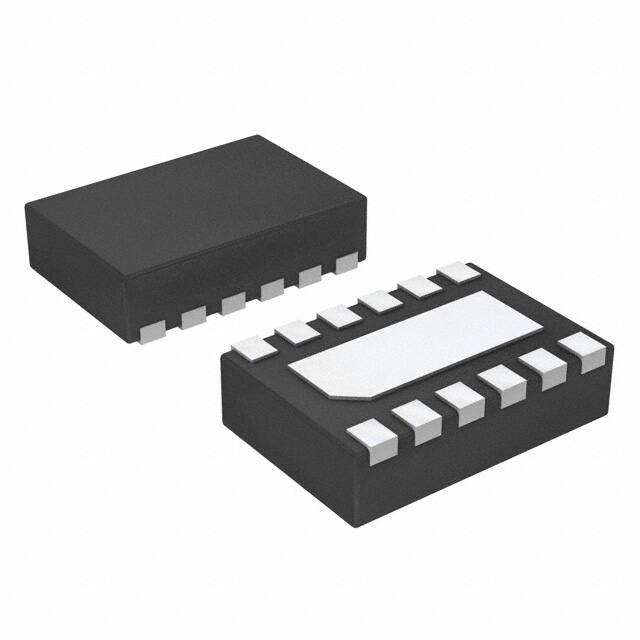
Product
Folder
Technical
Documents
Support &
Community
Tools &
Software
TPS25820, TPS25821
SLVSE24C – NOVEMBER 2017 – REVISED AUGUST 2019
TPS25820, TPS25821 USB Type-CTM 1.5-A Source Controller and Power Switch
1 Features
•
1
•
•
•
•
•
•
•
•
•
3 Description
The TPS25820/21 is a USB Type-C source controller
with an integrated 1.5 A-rated USB power switch. The
TPS25820/21 monitors the Type-C configuration
channel (CC) lines to determine when a USB sink is
attached. If a sink is attached, the TPS25820/21
applies power to VBUS and communicates the
selectable VBUS current sourcing capability to the sink
via the pass through CC line. If the sink is attached
with an electronically marked cable, the TPS25820
also applies VCONN power to the cable VCONN pin. The
TPS25821 does not apply VCONN power and is for
functions where VCONN is not needed such as USB
2.0 and data-less charging implementations.
TM
USB Type-C Rel. 1.3 Compliant Source
Controller
STD/1.5-A Current Capability Advertisement on
CC Lines
Connector Attach/Detach Detection
Super Speed Polarity Determination
VBUS and VCONN (TPS25820) Application and
Discharge with Internal Fixed Current Limit
1.0-µA (typ) Operating Current with Nothing
Attached to the Type-C Connector
64-mΩ (typ) High-Side OUT MOSFET
Meets USB Current-Limiting Requirements
– 1.7-A OUT Current Limit with ±7% Accuracy
– Fast Overcurrent Response – 1.5 μs (Typical)
CC1 and CC2 ±8-kV Contact and ±15-kV Air
Discharge ESD Rating (IEC-61000-4-2)
IEC/UL Certificates
– US-33101-UL: IEC 60950-1:2005;
AMD1:2009, AMD2:2013
– US-33102-UL: IEC 62368-1:2014
The TPS25820/21 draws 1.0 μA (typ) when nothing is
attached. The FAULT output signals when the switch
is in an overcurrent or overtemperature condition. The
SINK output signals when a sink is attached and the
POL output signals the polarity of the cable superspeed lines.
Device Information(1)
PART NUMBER
•
•
BODY SIZE (NOM)
WSON (12)
3.00 mm x 2.00 mm
TPS25821
WSON (12)
3.00 mm x 2.00 mm
(1) For all available packages, see the orderable addendum at
the end of the data sheet.
2 Applications
•
•
•
PACKAGE
TPS25820
USB 2.0 or 3.x Type-C Host and Hub Ports
Notebook/Desktop PCs and Tablets
LCD Monitor/Docking Station and Charging
Cradles
Type-C USB Wall Chargers, Power Bank, and
CLAs
Set-Top Box and Audio/Video Systems
Device Comparison
PART NUMBER
VCONN
TPS25820
Yes
TPS25821
No
Simplified Schematic
3 x 100 NŸ
Bus Power
4.5 V ± 5.5V
TPS25820/21
OUT
IN
Control Signals
VBUS
Power Switch
Status Signals
CHG
CC1
USB Type-C
Connector
FAULT
EN
CC2
SINK
POL
Type- C DFP
Status Signals
REF
100 NŸ
GND
Thermal Pad
Copyright
Copyright©
©2017,
2017,Texas
TexasInstruments
InstrumentsIncorporated
Incorporated
1
An IMPORTANT NOTICE at the end of this data sheet addresses availability, warranty, changes, use in safety-critical applications,
intellectual property matters and other important disclaimers. PRODUCTION DATA.
�TPS25820, TPS25821
SLVSE24C – NOVEMBER 2017 – REVISED AUGUST 2019
www.ti.com
Table of Contents
1
2
3
4
5
6
7
Features ..................................................................
Applications ...........................................................
Description .............................................................
Revision History.....................................................
Pin Configuration and Functions .........................
Specifications.........................................................
1
1
1
2
3
4
6.1
6.2
6.3
6.4
6.5
6.6
6.7
4
4
4
5
5
7
9
Absolute Maximum Ratings ......................................
ESD Ratings ............................................................
Recommended Operating Conditions.......................
Thermal Information ..................................................
Electrical Characteristics...........................................
Switching Characteristics ..........................................
Typical Characteristics ..............................................
Detailed Description ............................................ 10
7.1
7.2
7.3
7.4
Overview .................................................................
Functional Block Diagrams .....................................
Feature Description.................................................
Device Functional Modes........................................
8
Application and Implementation ........................ 16
8.1 Application Information............................................ 16
8.2 Typical Applications ................................................ 16
9 Power Supply Recommendations...................... 22
10 Layout................................................................... 23
10.1 Layout Guidelines ................................................. 23
10.2 Layout Example .................................................... 24
11 Device and Documentation Support ................. 25
11.1
11.2
11.3
11.4
11.5
11.6
11.7
11.8
Device Support ....................................................
Documentation Support .......................................
Related Links ........................................................
Receiving Notification of Documentation Updates
Community Resources..........................................
Trademarks ...........................................................
Electrostatic Discharge Caution ............................
Glossary ................................................................
25
25
25
25
25
25
25
26
10
12
13
15
12 Mechanical, Packaging, and Orderable
Information ........................................................... 26
Changes from Revision B (February 2019) to Revision C
Page
4 Revision History
•
Added US-33102-UL: IEC 62368-1:2014 to the Features section ......................................................................................... 1
Changes from Revision A (December 2017) to Revision B
•
Page
Added the IEC/UL Certificate No. to the Features section..................................................................................................... 1
Changes from Original (November 2017) to Revision A
•
2
Page
Changed TPS25821 from Product Preview to Production Data ........................................................................................... 1
Submit Documentation Feedback
Copyright © 2017–2019, Texas Instruments Incorporated
Product Folder Links: TPS25820 TPS25821
�TPS25820, TPS25821
www.ti.com
SLVSE24C – NOVEMBER 2017 – REVISED AUGUST 2019
5 Pin Configuration and Functions
DSS Package
12-Pin WSON
Top View
IN
1
12
OUT
IN
2
11
CC2
CHG
3
10
GND
EN
4
9
CC1
FAULT
5
8
REF
SINK
6
7
POL
Thermal
Pad
Not to scale
Pin Functions
PIN
I/O
DESCRIPTION
NAME
NUMBER
IN
1, 2
I
Device input supply. VBUS internal power switch input supply. VCONN internal power switch input supply for the
TPS25820.
CHG
3
I
Charge logic input to select between standard USB or 1.5-A Type-C current sourcing ability.
EN
4
I
Logic input to turn the device on and off.
FAULT
5
O
Open-drain logic output that asserts when the device is in overtemperature and/or VBUS is in current limit condition.
SINK
6
O
Open-drain logic output that asserts when a Type-C Sink is identified on the CC lines.
POL
7
O
Open-drain logic output that signals which Type-C CC pin is connected to the cable CC line. This gives the
information needed to mux the super speed lines. Asserted when the CC2 pin is connected to the cable CC line.
REF
8
I
Analog input used to make a current reference. Connect a 0.5%, 100-ppm, 100-kΩ resistor between this pin and
GND.
CC1
9
I/O
GND
10
–
Analog input/output that connects to the Type-C receptacle CC1 pin.
CC2
11
I/O
Analog input/output that connects to the Type-C receptacle CC2 pin.
OUT
12
O
VBUS power switch output.
Thermal Pad
–
–
Thermal pad on bottom of package.
Ground
Copyright © 2017–2019, Texas Instruments Incorporated
Product Folder Links: TPS25820 TPS25821
Submit Documentation Feedback
3
�TPS25820, TPS25821
SLVSE24C – NOVEMBER 2017 – REVISED AUGUST 2019
www.ti.com
6 Specifications
6.1 Absolute Maximum Ratings
over operating free-air temperature range, voltages are respect to GND (unless otherwise noted)
Pin voltage, V
IN, EN, CHG, REF, OUT, FAULT, CC1, CC2, SINK, POL
Pin positive source current, ISRC
OUT, REF, CC1, CC2
(1)
MIN
MAX
UNIT
–0.3
6
V
Internally
limited
A
2.5
A
OUT (while applying VBUS)
CC1, CC2 (while TPS25820 applying VCONN)
Pin positive sink current, ISNK
FAULT, SINK, POL
1
A
Internally
limited
mA
Operating junction temperature, TJ
–40
180
°C
Storage temperature range, Tstg
–65
150
°C
(1)
Stresses beyond those listed under Absolute Maximum Ratings may cause permanent damage to the device. These are stress ratings
only, which do not imply functional operation of the device at these or any other conditions beyond those indicated under Recommended
Operating Conditions. Exposure to absolute-maximum-rated conditions for extended periods may affect device reliability.
6.2 ESD Ratings
VALUE
Human-body model (HBM), per ANSI/ESDA/JEDEC JS-001
V(ESD)
(1)
(2)
(3)
(4)
(1)
Electrostatic
discharge
(2)
UNIT
±2000
Charged-device model (CDM), per JEDEC specification JESD22-C101 (3)
±500
IEC61000-4-2 contact discharge, CC1 and CC2 (4)
±8000
IEC61000-4-2 air-gap discharge, CC1 and CC2 (4)
±15000
V
Electrostatic discharge (ESD) to measure device sensitivity/immunity to damage caused by assembly line electrostatic discharges into
the device.
JEDEC document JEP155 states that 500-V HBM allows safe manufacturing with a standard ESD control process.
JEDEC document JEP157 states that 250-V CDM allows safe manufacturing with a standard ESD control process.
Surges per IEC61000-4-2, 1999 applied between CC1/CC2 and output ground of the TPS25820EVM-835.
6.3 Recommended Operating Conditions
Voltages are with respect to GND (unless otherwise noted)
MIN
NOM
MAX
UNIT
VI
Supply voltage
IN
4.5
5.5
V
VI
Input voltage
EN, CHG
0
5.5
V
VIH
High-level input voltage
EN, CHG
2
VIL
Low-level voltage
EN, CHG
VPU
Pull-up voltage
Used on FAULT, SINK, POL
ISRC
Positive source current
ISNK
Positive sink current (100 ms
moving average)
0.8
V
5.5
V
OUT
1.5
A
CC1 or CC2 when supplying VCONN
250
mA
0
SINK, POL
5
FAULT
10
ISNK_PULSE Positive repetitive pulse sink current FAULT, SINK, POL
TJ
4
Operating junction temperature
Submit Documentation Feedback
V
–40
mA
Internally
Limited
mA
125
°C
Copyright © 2017–2019, Texas Instruments Incorporated
Product Folder Links: TPS25820 TPS25821
�TPS25820, TPS25821
www.ti.com
SLVSE24C – NOVEMBER 2017 – REVISED AUGUST 2019
6.4 Thermal Information
THERMAL METRIC
TPS25820,
TPS25821
(1)
UNIT
DSS (WSON)
12 PINS
RθJA
Junction-to-ambient thermal resistance
57.7
°C/W
RθJC(top)
Junction-to-case (top) thermal resistance
53.7
°C/W
RθJB
Junction-to-board thermal resistance
24.1
°C/W
ψJT
Junction-to-top characterization parameter
1.6
°C/W
ψJB
Junction-to-board characterization parameter
24.1
°C/W
RθJC(bot)
Junction-to-case (bottom) thermal resistance
7.4
°C/W
(1)
For more information about traditional and new thermal metrics, see the Semiconductor and IC Package Thermal Metrics application
report.
6.5 Electrical Characteristics
–40°C ≤ TJ ≤ 125°C, 4.5 V ≤ VIN ≤ 5.5 V, VEN = VCHG = VIN, RREF = 100 kΩ. Typical values are at 25°C. All voltages are with
respect to GND. IOUT and IOS defined positive out of the indicated pin (unless otherwise noted)
PARAMETER
TEST CONDITIONS
MIN
TYP
MAX
TJ = 25°C, IOUT = 1.5 A
64
70
–40°C ≤ TJ ≤ 85°C, IOUT = 1.5 A
64
85
–40°C ≤ TJ ≤ 125°C, IOUT = 1.5 A
64
98
0
3
1.72
1.84
UNIT
OUT - POWER SWITCH
RDS(on)
IREV
On resistance (1)
OUT to IN reverse leakage current
VOUT = 5.5 V, 0 ≤ VIN ≤ 5.5 V, VEN = 0 V,
–40°C ≤ TJ ≤ 85°C, measure IIN
mΩ
µA
OUT - CURRENT LIMIT
IOS
Short circuit current limit
1.6
(1)
RREF = 10 Ω
A
4.0
OUT - DISCHARGE
Discharge resistance
VOUT = 4 V
Bleed discharge resistance
VOUT = 4 V, No Sink termination on CC
lines, time > tw_OUT_DCHG
400
500
600
Ω
90
150
250
kΩ
800
mV
17.5
µA
0.82
V
250
mV
1
µA
Rising threshold for not
discharged
VTH
REF
IOS
Short circuit current
VO
Output voltage
RREF = 10 Ω
9.5
0.78
0.8
FAULT
VOL
Output low voltage
I FAULT = 1 mA
IOFF
Off-state leakage
V FAULT = 5.5 V
CC1/CC2 - VCONN POWER SWITCH (TPS25820)
RDS(on)
On resistance
TJ = 25°C, ICCx = 250 mA
480
530
-40°C ≤ TJ ≤ 85°C, ICCx = 250 mA
480
645
-40°C ≤ TJ ≤ 125°C, ICCx = 250 mA
480
755
370
425
mΩ
CC1/CC2 - VCONN POWER SWITCH - CURRENT LIMIT (TPS25820)
IOS
(1)
315
Short circuit current limit (1)
RREF = 10 Ω
1000
mA
Pulse-testing techniques maintain junction temperature close to ambient temperature; thermal effects must be taken into account
separately.
Copyright © 2017–2019, Texas Instruments Incorporated
Product Folder Links: TPS25820 TPS25821
Submit Documentation Feedback
5
�TPS25820, TPS25821
SLVSE24C – NOVEMBER 2017 – REVISED AUGUST 2019
www.ti.com
Electrical Characteristics (continued)
–40°C ≤ TJ ≤ 125°C, 4.5 V ≤ VIN ≤ 5.5 V, VEN = VCHG = VIN, RREF = 100 kΩ. Typical values are at 25°C. All voltages are with
respect to GND. IOUT and IOS defined positive out of the indicated pin (unless otherwise noted)
PARAMETER
TEST CONDITIONS
MIN
TYP
MAX
73
80
85
168
180
190
64
80
96
CCx is the CC pin under test, CCy is the
other CC pin. VCCx = 5.5 V, CCy floating,
VEN = 0 V or 0 V ≤ VIN ≤ 5.5 V, –40°C ≤ TJ
≤ 85°C, IREV is current into CCx pin.
0
5
CCx is the CC pin under test, CCy is the
other CC pin. VCCx = 5.5 V, CCy = 0
V, –40°C ≤ TJ ≤ 85°C, IREV is current
into CCx pin.
5
10
UNIT
CC1/CC2 – CONNECT MANAGEMENT
VCHG = 0 V, 0 V ≤ VCCx ≤ 1.5 V, after V
=0V
ISRC
SINK
0 V ≤ VCCx ≤ 1.5 V, after V SINK = 0 V
Sourcing current
VCHG = 0 V or VIN, 0 V ≤ VCCx ≤ 1.5
V, before V SINK = 0 V
IREV
Reverse leakage current
µA
µA
CC1/CC2 – CONNECT MANAGEMENT – VCONN DISCHARGE MODE
VTH
Discharge resistance (TPS25820)
CC pin that was providing VCONN before
detach: VCCX = 4 V
400
500
600
Ω
Falling threshold for discharged
(TPS25820)
CC pin that was providing VCONN before
detach
570
600
630
mV
Discharged threshold hysteresis
(TPS25820)
100
mV
SINK, POL
VOL
Output low voltage
ISNK_PIN = 1 mA
IOFF
Off-state leakage
VPIN = 5.5 V
250
mV
1
µA
1.8
V
EN, CHG - LOGIC INPUTS
VTH
Rising threshold voltage for output
logic change
VTH
Falling threshold voltage for output
logic change
1.45
1.00
Hysteresis (2)
IIN
Input current
VPIN = 0 V or 5.5 V
1.35
V
100
mV
–0.5
0.5
µA
OVER TEMPERATURE SHUT DOWN
TTH_OTSD2
Rising threshold temperature for
device shutdown
155
Hysteresis (2)
TTH_OTSD1
°C
20
Rising threshold temperature for
OUT/ VCONN switch shutdown in
current limit
°C
135
Hysteresis (2)
°C
20
°C
IN
VTH
Rising threshold voltage for
not UVLO
Hysteresis
(2)
6
3.9
(2)
4.1
100
4.3
V
mV
These parameters are provided for reference only and do not constitute part of TI’s published specifications for purposes of TI’s product
warranty.
Submit Documentation Feedback
Copyright © 2017–2019, Texas Instruments Incorporated
Product Folder Links: TPS25820 TPS25821
�TPS25820, TPS25821
www.ti.com
SLVSE24C – NOVEMBER 2017 – REVISED AUGUST 2019
Electrical Characteristics (continued)
–40°C ≤ TJ ≤ 125°C, 4.5 V ≤ VIN ≤ 5.5 V, VEN = VCHG = VIN, RREF = 100 kΩ. Typical values are at 25°C. All voltages are with
respect to GND. IOUT and IOS defined positive out of the indicated pin (unless otherwise noted)
PARAMETER
TEST CONDITIONS
Disabled supply current
VEN = 0 V, –40°C ≤ TJ ≤ 85°C
Enabled supply current with CC
lines open
–40°C ≤ TJ ≤ 85°C
MIN
II
VCHG = 0 V
Enabled supply current with Sink
attached via cable that is not
electronically marked (includes IN
current that provides the CC
output current to the sink Rd
resistor)
VCHG = 0 V
MAX
UNIT
1
Enabled supply current with
dangling Ra cable attached
Enabled supply current with Sink
attached via cable that is
electronically marked (includes IN
current that provides the CC
output current to the sink Rd
resistor)
TYP
1
4
150
195
232
275
332
380
210
250
310
355
µA
6.6 Switching Characteristics
–40°C ≤ TJ ≤ 125°C, 4.5 V ≤ VIN ≤ 5.5 V, VEN = VCHG = VIN, RREF = 100 kΩ. Typical values are at 25°C. All voltages are with
respect to GND. IOUT and IOS defined positive out of the indicated pin (unless otherwise noted)
PARAMETER
TEST CONDITIONS
MIN
TYP
MAX
UNIT
0.5
0.8
1.2
ms
0.2
0.3
0.4
ms
2.1
3.2
4.5
ms
0.8
1.3
1.9
ms
169
262
361
ms
1.5
4
µs
8.2
10.6
ms
OUT - POWER SWITCH
tr
Output voltage rise time
tf
Output voltage fall time
ton
Output voltage turn-on time
toff
Output voltage turn-off time
tw_OUT_DCHG
VIN = 5 V, CL = 1 µF, RL = 100 Ω
(measure between 10% and 90% of
final value)
VIN = 5 V, CL = 1 µF, RL = 100 Ω
RDCHG application time at OUT turn
off
VOUT = 1 V, time ISNK_OUT > 1 mA
after Sink termination removed from
CC lines
OUT - CURRENT LIMIT
tiOS
Current limit response time to short
circuit
VIN - VOUT = 1 V, RL = 10 mΩ (see
Figure 1)
FAULT
tDEGA
Asserting deglitch due to overcurrent
tDEGA
Asserting deglitch due to
overtemperature in current limit
tDEGD
De-asserting deglitch
5.6
0
ms
5.6
8.2
10.6
ms
0.13
0.22
0.3
ms
0.18
0.22
0.26
ms
1.4
2.2
3.2
ms
0.25
0.33
0.4
ms
42
65
90
ms
1
4
µs
CC1/CC2 - VCONN POWER SWITCH (TPS25820)
tr
Output voltage rise time
tf
Output voltage fall time
ton
Output voltage turn-on time
toff
Output voltage turn-off time
VIN2 = 5 V, CL = 1 µF, RL = 100 Ω
VIN2 = 5 V, CL = 1 µF, RL = 100 Ω
Minimum VCONN discharge time
TPS25820
CC1/CC2 - VCONN POWER SWITCH - CURRENT LIMIT (TPS25820)
tres
Current limit response time to short
circuit
VIN – VCCx = 1 V, R = 10 mΩ (see
Figure 1)
SINK, POL
tDEGA
Asserting deglitch
100
150
200
ms
tDEGD
De-asserting deglitch
7.9
12.5
17.7
ms
Copyright © 2017–2019, Texas Instruments Incorporated
Product Folder Links: TPS25820 TPS25821
Submit Documentation Feedback
7
�TPS25820, TPS25821
SLVSE24C – NOVEMBER 2017 – REVISED AUGUST 2019
www.ti.com
IOS
IOUT
tios
Figure 1. Output Short Circuit Parameter Diagram
8
Submit Documentation Feedback
Copyright © 2017–2019, Texas Instruments Incorporated
Product Folder Links: TPS25820 TPS25821
�TPS25820, TPS25821
www.ti.com
SLVSE24C – NOVEMBER 2017 – REVISED AUGUST 2019
6.7 Typical Characteristics
180
1.8
1.6
ILIM - Limit Current (mA)
Sourcing Current (PA)
160
140
SINK 0.5 A/0.9 A (USB default)
SINK 1.5A
120
100
80
60
-40
-20
0
20
40
60
80
100
TJ - Junction Temperature (oC)
120
1
VBUS ILIM
VCONN ILIM
0.8
0.6
0.2
-40
140
-20
0
D001
Figure 2. CC Sourcing Current to SINK vs Temperature
20
40
60
80
100
TJ - Junction Temperature (oC)
120
140
D002
Figure 3. ILIM for VBUS and VCONN vs Temperature
350
345
0.12
II - Enable Supply Current (PA)
IREV - Reverse Leakage Current (PA)
1.2
0.4
0.14
0.1
0.08
0.06
0.04
0.02
0
-40
1.4
340
335
330
325
320
315
310
Sink attached with passive cable
Sink attached with active cable
305
-20
0
20
40
60
80
100
TJ - Junction Temperature (oC)
120
300
-40
140
-20
0
D001
20
40
60
80
100
TJ - Junction Temperature (oC)
120
140
D004
Device = Disabled; (VOUT-VIN) =6.5V
Figure 4. OUT Reverse Leakage Current vs Temperature
Figure 5. Supply Current with SINK vs Temperature
690
660
85
RDS(ON) - ON Resistance (m:)
RDS(ON) - ON Resistance (m:)
90
80
75
70
65
60
55
50
-40
630
600
570
540
510
480
450
420
390
-20
0
20
40
60
80
100
TJ - Junction Temperature (oC)
120
140
360
-40
-20
D005
Figure 6. VBUS Current Limiting Switch On Resistance vs
Temperature
0
20
40
60
80
100
TJ - Junction Temperature (oC)
120
140
D006
Figure 7. VCONN Current Limiting Switch On Resistance vs
Temperature
Copyright © 2017–2019, Texas Instruments Incorporated
Product Folder Links: TPS25820 TPS25821
Submit Documentation Feedback
9
�TPS25820, TPS25821
SLVSE24C – NOVEMBER 2017 – REVISED AUGUST 2019
www.ti.com
7 Detailed Description
7.1 Overview
The TPS25820 and TPS25821 devices are highly integrated USB Type-C source controllers with built-in power
switches developed for the USB Type-C connector and cable. The TPS25820 supports VCONN, while the
TPS25821 does not. The devices provide all of the functionality needed to support a USB Type-C DFP in a
system where USB power delivery (PD) source capabilities (for example, VBUS > 5 V) are not implemented. The
devices are designed to be compliant to the USB Type‑C specification, release 1.3 which added new
requirements to discharge VCONN.
7.1.1 USB Type C Basic
For a detailed description of the Type-C spec refer to the USB-IF website to download the latest released
version. Some of the basic concepts of the Type-C spec that pertains to understanding the operation of the
TPS25820/21 (a Downward Facing Port, DFP device) are described as follows.
USB Type-C removes the need for different plug and receptacle types for host and device functionality. The
Type-C receptacle replaces both Type-A and Type-B receptacles since the Type-C cable is plug-able in either
direction between host and device. A host-to-device logical relationship is maintained via the configuration
channel (CC). Optionally hosts and devices can be either providers or consumers of power when USB PD
communication is used to swap roles.
All
•
•
•
USB Type-C ports operate in one of below three data modes:
Host mode: the port can only be host (also provider of power)
Device mode: the port can only be device (also consumer of power)
Dual-Role mode: the port can be either host or device
Port types:
• DFP (Downstream Facing Port): Host, specifically associated with flow of data (Host or Hub) in a USB link
• Source: Port that asserts Rp (pull-up resistor) on CC pin and provides power on VBUS when attached to a
Sink (device). At power-up a DFP is a source.
• UFP (Upstream Facing Port): Device, specifically associated with flow of data (device) in a USB link
• Sink: Port that asserts Rd (pull-down) on CC pin and consumes power from VBUS when attached. At powerup a UFP is a sink
• DRP (Dual-Role Port): Host or Device
Valid Source-to-Sink connections:
• Table 1 describes valid Source-to-Sink connections
• Source to Source or Sink to Sink have no function
Table 1. Valid Source-to-Sink Connections
POWER ROLES
SOURCE ONLY
SINK ONLY
DUAL ROLE POWER (DRP)
Source Only
Not allowed
Allowed
Allowed
Sink Only
Allowed
Not allowed
Allowed
Dual Role Power
(DRP)
Allowed
Allowed
Allowed
7.1.2 Configuration Channel
The function of the configuration channel is to detect connections and configure the interface across the USB
Type-C cables and connectors.
Functionally the Configuration Channel (CC) is used to serve the following purposes:
• Detect connect to the USB ports
• Resolve cable orientation and twist connections to establish USB data bus routing
• Establish Source and Sink roles between two connected ports
• Discover and configure power: USB Type-C current modes or USB Power Delivery
• Discovery and configure optional Alternate and Accessory modes
10
Submit Documentation Feedback
Copyright © 2017–2019, Texas Instruments Incorporated
Product Folder Links: TPS25820 TPS25821
�TPS25820, TPS25821
www.ti.com
•
SLVSE24C – NOVEMBER 2017 – REVISED AUGUST 2019
Enhances flexibility and ease of use
Typical flow of DFP to UFP configuration is shown in Figure 8:
Figure 8. DFP to UFP Connect Flow
7.1.3 Detecting a Connection
Sources and DRPs fulfill the role of detecting a valid connection over USB Type-C. Figure 9 shows a Source to
Sink connection made with Type-C cable. As shown in Figure 9, the detection concept is based on being able to
detect terminations in the product which has been attached. A pull-up and pull-down termination model is used. A
pull-up termination can be replaced by a current source.
• In the Source-Sink connection the Source monitors both CC pins for a voltage lower than the unterminated
voltage.
• A Sink advertises Rd on both its CC pins (CC1 and CC2).
• A powered cable advertises Ra on its VCONN pin.
Sink monitors for
connection
Source monitors for
connection
Cable
CC
Rp
Ra
Rp
Rp
Ra
Source monitors for
connection
Rp
Sink monitors for
connection
Figure 9. Source-Sink Connection Mechanism
Copyright © 2017–2019, Texas Instruments Incorporated
Product Folder Links: TPS25820 TPS25821
Submit Documentation Feedback
11
�TPS25820, TPS25821
SLVSE24C – NOVEMBER 2017 – REVISED AUGUST 2019
www.ti.com
7.2 Functional Block Diagrams
Current Sense
IN
IN
Current Sense
OUT
OTSD
Thermal
Sense
CC1
UVLO
Current Sense
CC2
EN
CC
Monitor
CHG
Current
Limit
FAULT
Charge
Pump
Gate
Control
REF
SINK
POL
Control
Logic
GND
Copyright © 2017, Texas Instruments Incorporated
Figure 10. TPS25820 Functional Block Diagram
12
Submit Documentation Feedback
Copyright © 2017–2019, Texas Instruments Incorporated
Product Folder Links: TPS25820 TPS25821
�TPS25820, TPS25821
www.ti.com
SLVSE24C – NOVEMBER 2017 – REVISED AUGUST 2019
Functional Block Diagrams (continued)
Current Sense
IN
OUT
OTSD
Thermal
Sense
IN
CC1
UVLO
CC2
EN
CC
Monitor
CHG
Current
Limit
FAULT
Charge
Pump
Gate
Control
REF
SINK
POL
Control
Logic
GND
Copyright © 2017, Texas Instruments Incorporated
Figure 11. TPS25821 Functional Block Diagram
7.3 Feature Description
Both the TPS25820 and TPS25821 are source (i.e. DFP) Type-C port controllers with integrated power switches
for VBUS. The TPS25820 also has integrated power switches for VCONN. Refer to the functional block diagrams
(Figure 10 and Figure 11). The TPS25820/21 devices do not support BC1.2 charging modes, because it does not
interact with USB D+ and D– data lines. However supporting DCP mode of BC1.2 can be easily accomplished in
data-less ports like wall chargers and CLAs by simply tying a 100-Ω resistor between the D+ and D- pins of the
Type-C connector.
The TPS25820 has a built-in VCONN current limiting switch and can be used to implement USB 3.1 DFP, whereas
the TPS25821 does not implement a VCONN current limiting switch hence is used in the implementation in USB
2.0 DFP ports or as a USB source only port. Other than the VCONN current limiting switch there are no other
functional differences between the TPS25820 and TPS25821.
7.3.1 Configuration Channel Pins CC1 and CC2
The TPS25820/21 devices have two pins, CC1 and CC2 that serve to detect an attachment to the port and
resolve cable orientation. These pins are also used to establish the current broadcast to a valid sink and
configure VCONN (TPS25820 only).
Copyright © 2017–2019, Texas Instruments Incorporated
Product Folder Links: TPS25820 TPS25821
Submit Documentation Feedback
13
�TPS25820, TPS25821
SLVSE24C – NOVEMBER 2017 – REVISED AUGUST 2019
www.ti.com
Feature Description (continued)
Table 2 lists the TPS25820/21 response to various attachments to its port.
Table 2. Response to Attachments
TPS25820/21 RESPONSE (1)
TPS25820/21 TYPE-C PORT
CC1
CC2
Nothing Attached
OPEN
Sink Connected
Rd
OUT
VCONN (2)
On CC1 or CC2
POL
OPEN
OPEN
NO
Hi-Z
Hi-Z
OPEN
IN
NO
Hi-Z
LOW
SINK
Sink Connected
OPEN
Rd
IN
NO
LOW
LOW
Powered Cable/No Sink Connected
OPEN
Ra
OPEN
NO
Hi-Z
Hi-Z
Powered Cable/No Sink Connected
Ra
OPEN
OPEN
NO
Hi-Z
Hi-Z
Powered Cable/Sink Connected
Rd
Ra
IN
CC2
Hi-Z
LOW
Powered Cable/Sink Connected
Ra
Rd
IN
CC1
LOW
LOW
Debug Accessory Connected
Rd
Rd
OPEN
NO
Hi-Z
Hi-Z
Audio Adapter Accessory Connected
Ra
Ra
OPEN
NO
Hi-Z
Hi-Z
(1)
(2)
POL and SINK are open drain outputs; pull high with 100 kΩ to IN when used. Tie to GND or leave open when not used.
TPS25820 Only
7.3.2 Current Capability Advertisement and VBUS Overload Protection
The TPS25820/21 supports two Type-C current advertisements as defined by the USB Type-C standard. Current
broadcast to a connected Sink is controlled by the CHG pin. For each broadcast level the device protects itself
from a Sink that draws current in excess of the port’s USB Type-C Current advertisement by setting the current
limit as shown in Table 3.
Table 3. USB Type-C Current Advertisement
CHG
CC CAPABILITY BROADCAST
CURRENT LIMIT
0
STD (500 mA for USB 2.0 port)
1.67 A
0
STD (900 mA for USB 3.1 port)
1.67 A
1
1.5 A
1.67 A
Under overload conditions, the internal current-limit regulator limits the output current on the OUT pin as shown
in the Electrical Characteristics table. When an overload condition is present, the device maintains a constant
output current, with the output voltage determined by (IOS x RLOAD). Two possible overload conditions can occur.
The first overload condition occurs when either: 1) input voltage is first applied, enable is true, and a short circuit
is present (load which draws IOUT > IOS), or 2) input voltage is present and the TPS25820/21 is enabled into a
short circuit. The output voltage is held near zero potential with respect to ground and the TPS25820/21 ramps
the output current to IOS.
In either case the TPS25820/21 will limit the load current to IOS until the overload condition is removed or the
device begins to thermal cycle. This is demonstrated in Figure 16 where the device was enabled into a short, and
subsequently cycles current off and on as the thermal protection engages.
7.3.3 FAULT Response
The FAULT pin is an open drain output that asserts (active low) after a deglitch time (tDEGA) when device OUT
current exceeds its programmed value and/or overtemperature threshold is crossed. The FAULT signal remains
asserted until the fault condition is removed for tDEGD. The TPS25820/21 are designed to eliminate false
overcurrent fault reporting by using an internal deglitch circuit.
Connect FAULT with a 100-kΩ pull-up resistor to IN. FAULT can be left open or tied to GND when not used.
14
Submit Documentation Feedback
Copyright © 2017–2019, Texas Instruments Incorporated
Product Folder Links: TPS25820 TPS25821
�TPS25820, TPS25821
www.ti.com
SLVSE24C – NOVEMBER 2017 – REVISED AUGUST 2019
7.3.4 Thermal Shutdown
The device has two internal overtemperature shutdown thresholds, TTH_OTSD1 and TTH_OTSD2, to protect the
internal FET from damage and overall safety of the system. When the device temperature exceeds TTH_OTSD1,
any switch in current limit (OUT switch or VCONN switch) is disabled. The device does auto-retry recovery by reenabling the switch when die temperature decreases by 20°C. When TTH_OTSD2 is exceeded all open drain
outputs are left open and the device is disabled such that minimum power/heat is dissipated. The device does
auto-retry recovery by attempting to power-up when die temperature decreases by 20°C.
7.3.5 REF
A 100-kΩ resistor is connected from this pin to GND. This pin sets the reference current required to bias the
internal circuitry of the device. The overload current limit tolerance and CC currents depend upon the accuracy of
this resistor. A ±0.5% low temp CO resistor, or better, yields the best current limit accuracy and overall device
performance. If the CC capability broadcast will only be set to STD (CHG pulled low) then up to a ±10% resistor
may be used as long as the additional error in the current limit is acceptable.
7.3.6 Plug Polarity Detection
Reversible Type-C plug orientation is reported by the POL pin when a Sink is connected, however when no Sink
is attached, POL remains de-asserted irrespective of cable plug orientation. Table 2 describes the POL state
based on which device CC pin detects VRd from an attached Sink pull-down. In a typical USB 3.x DFP port, this
pin controls a superspeed data MUX for proper data connectivity irrespective of plug orientation. See Figure 20.
7.3.7 Sink Attachment Indicator
The attachment of a Type-C sink is reported by SINK. See Table 2.
7.3.8 Device Enable Control
The logic enable pin controls the power switch and device supply current. The supply current is reduced to less
than 1 μA when a logic low is present on EN. The EN pin provides a convenient way to turn on or turn off the
device while it is powered. When this pin is pulled high, the device is turned on or enabled. When the device is
disabled (EN pulled low), the internal FETs tied to IN are disconnected, all open drain outputs are left open (HiZ), and the CC1/CC2 monitor block is turned off. The EN pin should not be left floating.
7.3.9 Undervoltage Lockout (UVLO)
The undervoltage lockout (UVLO) circuit disables the power switch until the input voltage reaches the UVLO turnon threshold. Built-in hysteresis prevents unwanted on/off cycling due to input voltage droop during turn on.
7.4 Device Functional Modes
The TPS25820/21 is a Type-C controller with integrated power switch that supports all Type-C functions in a
downstream facing port (DFP). It is also used to manage current advertisement and protection to a connected
sink and active cable. The device starts its operation by monitoring the IN bus. When IN exceeds the
undervoltage lockout threshold, the device samples the EN pin. A high level on this pin enables the device and
normal operation begins. Having successfully completed its start-up sequence, the device now actively monitors
its CC1 and CC2 pins for attachment to a sink. When a sink is detected on either the CC1 or CC2 pin the internal
MOSFET starts to turn-on after the required de-bounce time is met. The internal MOSFET starts conducting and
allows current to flow from IN to OUT. For the TPS25820 if Ra is detected on the other CC pin (not connected to
sink), VCONN is applied to allow current to flow from IN to the CC pin connected to Ra. For a complete listing of
various device operational modes refer to Table 2.
Copyright © 2017–2019, Texas Instruments Incorporated
Product Folder Links: TPS25820 TPS25821
Submit Documentation Feedback
15
�TPS25820, TPS25821
SLVSE24C – NOVEMBER 2017 – REVISED AUGUST 2019
www.ti.com
8 Application and Implementation
NOTE
Information in the following applications sections is not part of the TI component
specification, and TI does not warrant its accuracy or completeness. TI’s customers are
responsible for determining suitability of components for their purposes. Customers should
validate and test their design implementation to confirm system functionality.
8.1 Application Information
The TPS25820/21 are Type-C source controllers. The TPS25820 supports all Type-C DFP required functions to
support a USB 3.x port and the TPS25821 supports all required functions for a USB 2.0 DFP. The TPS25820/21
only applies power to VBUS when it detects a sink is attached and removes power when it detects the sink is
detached. The device exposes its identity via its CC pin advertising its current capability based on the CHG pin
setting. The TPS25820/21 also limits its advertised current internally and provides robust protection against faults
on the system VBUS power rail.
After a connection is established by the TPS25820/21, the TPS25820/21 device is capable of providing VCONN to
power circuits in the cable plug on the CC pin that is not connected to the CC wire in the cable. VCONN is
internally current limited. The TPS25820/21 do not support Type-C optional accessory modes (Ra/Ra and Rd/Rd
in Table 2).
The following design procedure can be used to implement a full featured Type-C source.
8.2 Typical Applications
8.2.1 Type-C Source Port Implementation without BC 1.2 Support
Figure 12 shows a minimal Type-C source implementation capable of supporting 5-V and 1.5-A charging.
TPS25820/21
Bus Power 4.5V t 5.5V
0.1µF
47µF
47µF
47µF
CC1
CC2
SINK
POL
REF
100 k:
(1%)
GND
VBUS
Power Switch
Status Signal
OUT
FAULT
Type-C DFP
Status Signals
USB Type-C
Connector
IN
EN
Control Signals
CHG
3 x 100 k:
(Optional)
10µF
Power Pad
Copyright © 2017, Texas Instruments Incorporated
Figure 12. Type-C Source Port Implementation without BC 1.2 Support
8.2.1.1 Design Requirements
8.2.1.1.1
Input and Output Capacitance Considerations
Input and output capacitance improves the performance of the device. The actual capacitance should be
optimized for the particular application. For all applications, a 0.1-μF or greater ceramic bypass capacitor
between IN and GND is recommended as close to the device as possible for local noise decoupling.
All protection circuits, including those of the TPS25820/21 device, have the potential for input voltage overshoots
and output voltage undershoots. Input voltage overshoots can be caused by either of two effects. The first cause
is an abrupt application of input voltage in conjunction with input power-bus inductance and input capacitance
when the IN pin is high-impedance (before OUT turn-on, i.e. not connected to a Type-C sink device).
Theoretically, the peak voltage is 2 times the applied voltage. The second cause is due to the abrupt reduction of
16
Submit Documentation Feedback
Copyright © 2017–2019, Texas Instruments Incorporated
Product Folder Links: TPS25820 TPS25821
�TPS25820, TPS25821
www.ti.com
SLVSE24C – NOVEMBER 2017 – REVISED AUGUST 2019
Typical Applications (continued)
output short-circuit current when the device turns off and energy stored in the input inductance drives the input
voltage high. Input voltage droops may also occur with large load steps and as the output is shorted. Applications
with large input inductance (for instance, connecting the evaluation board to the bench power supply through
long cables) may require large input capacitance to prevent the voltage overshoot from exceeding the absolute
maximum voltage of the device.
The fast current-limit speed of the TPS25820/21 device to hard output short circuits isolates the input bus from
faults. However, ceramic input capacitance in the range of 1 μF to 22 μF adjacent to the input aids in both
response time and limiting the transient seen on the input power bus. Output voltage undershoot is caused by
the inductance of the output power bus just after a short has occurred and the device has abruptly reduced the
OUT current. Energy stored in the inductance drives the OUT voltage down, and potentially negative, as it
discharges. An application with large output inductance (such as from a cable) benefits from the use of a highvalue output capacitor to control voltage undershoot.
Since the source is considered cold socketed when not attached to a sink, the output capacitance should be
placed at the IN pin rather than the OUT pin, which has been commonly used in USB Type-A ports. A 120-μF
capacitance is recommended in this situation. It is also recommended to a ceramic capacitor less than 10 μF on
the OUT pin for better voltage bypass and compliance to Type-C spec.
8.2.1.1.2 System Level ESD Protection
System-level ESD (per EN61000-4-2) may occur as the result of a cable being plugged in, or a user touching the
USB receptacle or cable plug exposed pins. The recommended capacitor on the OUT pin helps reduce the
severity of ESD hit on the VBUS path thereby protecting the OUT pin of device. The device has ESD protection
built into the CC1 and CC2 pins so that no external protection is necessary as long as proper trace layout
guidelines are practiced. Refer to the Layout Guidelines section for external component placement and routing
recommendations.
8.2.1.2 Detailed Design Procedure
Design considerations are listed below:
• Place at least 120 µF of bypass capacitance close to the IN pins versus OUT as Type C is a cold socket
connector.
• A


 工商网监
湘ICP备2023018690号
工商网监
湘ICP备2023018690号
