www.ti.com
Table of Contents
User’s Guide
TPS5124 Buck Controller Evaluation Module User's Guide
Table of Contents
1 Introduction.............................................................................................................................................................................2
2 Features...................................................................................................................................................................................2
3 Schematic................................................................................................................................................................................3
4 Design Procedure................................................................................................................................................................... 4
4.1 Frequency Setting.............................................................................................................................................................. 4
4.2 Inductance Value................................................................................................................................................................4
4.3 Output Capacitors.............................................................................................................................................................. 4
4.4 Input Capacitors................................................................................................................................................................. 4
4.5 Compensation Design........................................................................................................................................................6
4.6 Current Limiting..................................................................................................................................................................7
4.7 Timer Latch........................................................................................................................................................................ 7
5 Test Results.............................................................................................................................................................................9
5.1 Efficiency Curves................................................................................................................................................................9
5.2 Typical Operating Waveform.............................................................................................................................................. 9
5.3 Start-Up Waveform.............................................................................................................................................................9
5.4 Output Ripple Voltage and Load Transient...................................................................................................................... 10
6 Layout Guidelines.................................................................................................................................................................12
6.1 Low-Side MOSFET.......................................................................................................................................................... 12
6.2 Connections..................................................................................................................................................................... 12
6.3 Bypass Capacitor............................................................................................................................................................. 12
6.4 Bootstrap Capacitor......................................................................................................................................................... 12
6.5 Output Voltage................................................................................................................................................................. 12
7 PCB Layout............................................................................................................................................................................13
8 List of Materials.....................................................................................................................................................................16
9 Revision History................................................................................................................................................................... 16
Trademarks
All trademarks are the property of their respective owners.
SLUU182A – JANUARY 2004 – REVISED MARCH 2022
TPS5124 Buck Controller Evaluation Module User's Guide
Submit Document Feedback
Copyright © 2022 Texas Instruments Incorporated
1
�Introduction
www.ti.com
1 Introduction
The TPS5124 is a dual independent synchronous buck controller. Both controllers internal to the TPS5124
operate at 180° phase shift and the input ripple is partially canceled, therefore, the required input capacitance is
reduced. Other features include a separate soft-start circuit and standby control. See the TPS5124 Dual Channel
Synchronous Step-Down PWM Controller Data Sheet for detail.
2 Features
This EVM is designed to operate from 12-V bus voltage. It generates two outputs: 3.3 V at 15 A and 1.5 V at 10
A.
Table 2-1. TPS5124EVM-001 Performance Summary
Parameter
Test Conditions
Input voltage range
MIN
TYP
MAX
Units
6.5
12.0
15.0
V
Operating frequency
300
kHz
92
mV
Input ripple voltage (RMS)
VIN = 12 V, IOUT1 = 15 A, IOUT2 = 10 A
Output current range
6.5 V ≤ VIN ≤ 15 V
Line regulation
6.5 V ≤ VIN ≤ 15 V, IOUT = 15 A
±0.1%
Load regulation
1 A ≤ IOUT ≤ 15 A, VIN = 12 V
±0.3%
Load transient response
voltage change
IOUT rising from 0 A to 8.5 A
−160
IOUT falling from 8.5 A to 0 A
200
Load transient response
recovery time
IOUT rising from 0 A to 8.5 A
80
IOUT falling from 8.5 A to 0 A
120
Loop bandwidth
IOUT = 15 A
30
kHz
Phase margin
IOUT = 15 A
55
°
Output ripple voltage
IOUT = 15 A
Output rise time
VIN = 12 V, VOUT = 3.3 V, IOUT = 15 A
2.85
Full load efficiency
VIN = 12 V, VOUT = 3.3 V, IOUT = 15 A
90.6%
Channel 1
0
15
33
16
A
mVPK
ms
66
mVPP
ms
Channel 2
2
Output current range
6.5 V ≤ VIN ≤ 15 V
Line regulation
6.5 V ≤ VIN ≤ 15 V
0
±0.1%
10
Load regulation
1 A ≤ IOUT ≤ 10 A, VIN = 12 V
±0.3%
Load transient response
voltage change
IOUT rising from 0 A to 7.5 A
−120
IOUT falling from 7.5 A to 0 A
220
Load transient response
recovery time
IOUT rising from 0 A to 7.5 A
40
IOUT falling from 7.5 A to 0 A
80
Loop bandwidth
IOUT = 10 A
23
kHz
Phase margin
IOUT = 10 A
55
°
Output ripple voltage
IOUT = 10 A
Output rise time
VIN = 12 V, VOUT = 1.5 V, IOUT = 10 A
2.12
Full load efficiency
VIN = 12 V, VOUT = 1.53 V, IOUT = 10 A
85.5%
15
TPS5124 Buck Controller Evaluation Module User's Guide
12
A
mVPK
ms
30
mVPP
ms
SLUU182A – JANUARY 2004 – REVISED MARCH 2022
Submit Document Feedback
Copyright © 2022 Texas Instruments Incorporated
�www.ti.com
Schematic
3 Schematic
+
+
Figure 3-1. HPA053 TPS5124 Controller Schematic
SLUU182A – JANUARY 2004 – REVISED MARCH 2022
TPS5124 Buck Controller Evaluation Module User's Guide
Submit Document Feedback
Copyright © 2022 Texas Instruments Incorporated
3
�Design Procedure
www.ti.com
4 Design Procedure
4.1 Frequency Setting
Many factors influence frequency selection. Higher switching frequency leads to smaller output inductor and
capacitors, reducing the size of the converter. However, higher switching frequencies increase switching losses,
and lower the efficiency of the converter. A frequency of 300 kHz is chosen for this design for reasonable
efficiency and size.
Capacitor C16, which is connected from CT (pin 5) to ground, programs the oscillator frequency. A C16 value of
47 pF yields a switching frequency of 300 kHz at 25°C.
4.2 Inductance Value
The inductance value can be calculated using Equation 1.
where
•
L=
VOUT
V
× 1 − V OUT
f min × IRIPPLE
IN max
(1)
IRIPPLE is the ripple current flowing through the inductor.
The ripple current affects the output voltage ripple and core losses. Based on 20% ripple current and 300 kHz,
the inductance value is calculated as 2.2 μH. An off-the-shelf 2.2-μH inductor from Vishay is chosen. The part
number is IHLP−5050CE−01−2R2M01. The DCR is 7 mΩ and the DCR-related conduction loss is 1.6 W, which
is about 3.3% of output power.
The same procedure is followed to choose the inductor for Channel 2. The same inductor is chosen.
4.3 Output Capacitors
The required output capacitance and its ESR can be calculated using Equation 2 and Equation 3.
I
COUT min = 8 × f RIPPLE
× VRIPPLE
(2)
V
ESROUT = I RIPPLE
(3)
RIPPLE
With 1% output voltage ripple, the required minimum output capacitance is 54 μF and its ESR should be less
than 7.7 mΩ.
From the load transient point of view, the capacitance needed for 6% overshoot can be calculated using
Equation 4.
COUT =
where
•
•
2
IOUT max × L
2
2
VOUT2 − VOUT1
(4)
VOUT2 is the allowed overshoot voltage.
VOUT1 is the nominal operating voltage.
For 6% overshoot, the required capacitance is about 370 μF. Four 100-μF, 6.3-V ceramic capacitors are used.
Their ESR value is 2.0 mΩ each.
4.4 Input Capacitors
Due to the out-of-phase operation, the input current ripple is partially canceled. The total RMS current in the
input capacitor is calculated as follows. This assumes the total input current goes into the input capacitor to the
power ground and ignores the ripple current in the inductor.
4
TPS5124 Buck Controller Evaluation Module User's Guide
SLUU182A – JANUARY 2004 – REVISED MARCH 2022
Submit Document Feedback
Copyright © 2022 Texas Instruments Incorporated
�www.ti.com
Design Procedure
(IOUT1 - IAVG)
(IOUT2 - IAVG)
0V
I AVG
0
I AVG
T D2 x T
+
2
T
2
D1 x T
T
UDG−04010
Figure 4-1. Case One (D1 < 0.5, D2 < 0.5)
(IOUT1 + IOUT2 - IAVG)
(IOUT1 - IAVG)
(IOUT2 - IAVG)
0V
I AVG
D1 x T
T
2
0
T + D2 x T T
2
UDG−04010
Figure 4-2. Case Two (D2 < 0.5 < D1)
4.4.1 Case One: D1, D2 < 0.5
The ripple current through the input capacitor is shown in Figure 4-1 and can be calculated using Equation 5.
IincapRMS
(5)
T + D2 × T
T
T
2
D1 × T
2
2
2
2
1
= T
× ∫0
IOUT1 − IAVG dt + ∫ 2
IAVG dt + ∫ T
IOUT2 − IAVG dt + ∫ T + D2 × T IAVG dt
D1 × T
2
2
where
•
IincapRMS = D1 × IOUT1
2
+ D2 × IOUT2
2
2
− IAVG
(6)
IAVG is the average input current.
IAVG = IOUT1× D1 + IOUT2 × D2
(7)
4.4.2 Case Two: D2 < 0.5 < D1
The ripple current through the input capacitor is shown in Section 4.4 and can be calculated using Equation 8.
T
T + D2 × T
D1 × T
T
2
2
2
2
1
2 I
2
T
×
∫
−
I
dt
+
∫
I
+
I
−
I
dt
+
∫
IOUT2 − IAVG dt + ∫ T + D2 × T IAVG dt
OUT1
AVG
OUT1
OUT2
AVG
T
0
D1 × T
2
2
IincapRMS = D1 × IOUT1
2
+ D2 × IOUT2
2
2
+ 2 × D1 − 1 × IOUT1 × IOUT2 − IAVG
(9)
SLUU182A – JANUARY 2004 – REVISED MARCH 2022
TPS5124 Buck Controller Evaluation Module User's Guide
Submit Document Feedback
Copyright © 2022 Texas Instruments Incorporated
5
�Design Procedure
www.ti.com
This EVM meets “Case One” criteria. The maximum input ripple current is 6.7 A at VIN = 12 V. Two 150-μF, 20-V
special polymer capacitors from Panasonic (part number is EEFWA1D151P) are used. It can handle 3.7 A of
ripple current each. The ESR value of each capacitor is 26 mΩ. So the input ripple voltage is calculated using
Equation 10 and is approximately 88 mVRMS.
IRIPPLE = IincapRMS × ESR
(10)
4.5 Compensation Design
The following compensation loop design uses Channel 1 as example, but a design for Channel 2 follows the
same rules.
The TPS5124 uses voltage-mode control method. A Type III compensation network, formed by R1, R2, R4, C14,
C12, and C23, is used to ensure the stability. The L-C frequency of the power stage is around 5.4 kHz and the
ESR zero is at 790 KHz due to the low ESR of the ceramic capacitors. An overall crossover frequency (f0db) of
30 kHz is chosen for reasonable transient response and stability. Both zeros (f Z1 and f Z2) from the compensator
are set at 2.68 kHz. The two poles (f P1 and f P2) and are set at 150 kHz and 2 MHz. The frequency of poles and
zeros are defined by the following equations.
1
fZ1 = 2π × R4
× C14
where
•
(11)
1
fZ2 = 2π × R1
× C12
(12)
R1 >> R2 is assumed.
1
fP1 = 2π × R4
× C23
where
•
(13)
1
fP2 = 2π × R2
× C12
(14)
C14 >> C23 is assumed.
The transfer function for the compensator is calculated as:
A s =
6
1 + s × C14 × R2 × 1 + s × C12 × R1 + R2
s × R1 × C14 × 1 + C23
C14 + s × R4 × C23 × 1 + s × R2 × C12
TPS5124 Buck Controller Evaluation Module User's Guide
(15)
SLUU182A – JANUARY 2004 – REVISED MARCH 2022
Submit Document Feedback
Copyright © 2022 Texas Instruments Incorporated
�www.ti.com
Figure 4-3. Gain and Phase vs Oscillator
Frequency (Channel 1)
Design Procedure
Figure 4-4. Gain and Phase vs Oscillator
Frequency (Channel 2)
Figure 4-3 shows the closed loop gain and phase. For Channel 1, the overall crossover frequency is
approximately 30 kHz and the phase margin is 58°. For Channel 2, the crossover frequency is approximately 23
kHz and phase margin is 55°.
4.6 Current Limiting
The current limit in the TPS5124 is set using an internal current source and an external resistor (R13 and R14).
The current limit protection circuit compares the drain-to-source voltage of the high-side and low-side drivers
with respect to the set-point voltage. If the voltage exceeds the limit during high-side conduction, the current limit
circuit terminates the high-side driver pulse. If the set point voltage is exceeded during low-side conduction, the
low-side pulse is extended through the next cycle. Together, this action has the effect of decreasing the output
voltage until the undervoltage protection circuit is activated and the fault latch is set and both the high-side and
low-side MOSFET drivers are shut off. Equation 16 should be used for calculating the external resistor value for
current protection set point.
where
•
•
•
•
•
I
1.3 × RDS on × ILIM + RIPPLE
2
RCL =
ITRIP
(16)
RCL is the external current limit resistor (R13 and R14).
RDS(on) is the on-resistor of the low-side MOSFET (Q2 and Q4).
1.3 is the temperature coefficient of RDS(on).
ILIM is the required current limit.
ITRIP is the internal current source with a typical value of 13 μA at 25°C.
4.7 Timer Latch
The TPS5124 includes fault latch function with a user-adjustable timer to latch the MOSFET drivers in case of
a fault condition. When either the OVP or UVP comparator detects a fault condition, the timer starts to charge
C18, the external capacitor connected to the SCP pin. The circuit is designed so that for any value of C18, the
undervoltage latch time, tUVPL, is about five times larger than the overvoltage latch time tOVPL. The equations
needed to calculate the required value of C18 for the desired overvoltage and undervoltage latch delay times are
calculated in Equation 17 and Equation 18.
tUVPL
C18 = 1.7 × 10−6 × 1.185
(17)
SLUU182A – JANUARY 2004 – REVISED MARCH 2022
TPS5124 Buck Controller Evaluation Module User's Guide
Submit Document Feedback
Copyright © 2022 Texas Instruments Incorporated
7
�Design Procedure
www.ti.com
t
where
•
•
•
OVPL
C18 = 8 × 10−6 × 1.185
(18)
C18 is the external capacitor connected to the SCP pin.
tUVPL is the time from UVP detection to latch.
tOVPL is the time from OVP detection to latch.
For the EVM, tUVPL = 7 ms and tOVPL = 1.5 ms, so C18 = 0.01 μF.
If the voltage on the SCP pin reaches 1.185 V, the fault latch is set, and the MOSFET drivers are set as follows.
4.7.1 Undervoltage Protection
The undervoltage comparator circuit continually monitors the voltage at the INV pin. If the voltage at that pin falls
below 78% of the 0.85-V reference, the timer begins to charge C18. If the fault condition persists beyond the
time tUVPL, the fault latch is set and both the high-side and low-side drivers is forced OFF.
4.7.2 Short Circuit Protection
The short circuit protection circuitry uses the UVP circuit to latch the MOSFET drivers. When the current
limit circuit limits the output current, then the output voltage goes below the target output voltage and UVP
comparator detects a fault condition as described above.
4.7.3 Overvoltage Protection
The overvoltage comparator circuit continually monitors the voltage at the INV pin. If VINV rises above 112% of
the 0.85-V reference, the timer begins to charge C18. If the fault condition persists beyond the time tOVPL, the
fault latch is set and the high-side drivers are forced OFF, while the low-side drivers are forced ON.
CAUTION
Do not set the SCP terminal to a voltage lower than 1.185 V while the device is timing out an OVP
or UVP event. If the SCP terminal is manually set to a voltage lower than 1.185 V during this time,
output overshoot can occur. The TPS5124 must be reset by grounding STBYx.
4.7.4 Disabling the Protection Function
If it is necessary to disable the protection functions of the TPS5124 for troubleshooting or other purposes, the
OCP, OVP, and UVP circuits can be disabled.
4.7.4.1 Disabling the Overcurrent Protection
Remove the current limit resistors R13 and R14 to disable the current limit function.
4.7.4.2 Disabling the Overvoltage Protection or Undervoltage Protection
Grounding the SCP terminal can disable OVP and UVP.
8
TPS5124 Buck Controller Evaluation Module User's Guide
SLUU182A – JANUARY 2004 – REVISED MARCH 2022
Submit Document Feedback
Copyright © 2022 Texas Instruments Incorporated
�www.ti.com
Test Results
5 Test Results
5.1 Efficiency Curves
The efficiency was tested under three different operation conditions.
92
96
VIN = 6.5 V
VIN = 6.5 V
90
94
Percent Efficiency − %
Percent Efficiency − %
95
VIN = 12 V
93
92
91
88
86
VIN = 12 V
84
82
VIN = 15 V
80
90
78
VIN = 15 V
76
89
0
3
6
9
IOUT − Output Current − A
12
0
15
2
4
6
8
10
IOUT − Output Current − A
Figure 5-1. Overall Efficiency vs Output Current
VOUT1 (3.3 V) Enabled Only
Figure 5-2. Overall Efficiency vs Output Current
VOUT1 (1.5 V) Enabled Only
96
Percent Efficiency − %
94
VIN = 6.5 V
92
90
VIN = 15 V
88
VIN = 12 V
86
0
0.2
0.4
0.6
0.8
Output Power Over the Full Power
1.0
Figure 5-3. Overall Efficiency vs Output Power with Both Channels Enabled
5.2 Typical Operating Waveform
Figure 5-4 shows the typical operating waveforms taken at VIN = 12 V, IOUT1 = 15 A, and IOUT2 = 10 A.
5.3 Start-Up Waveform
Figure 5-5 shows the start-up waveform taken at VIN = 12 V, IOUT1 = 15 A, and IOUT2 = 10 A. The rising time is
2.85 ms for VOUT1 and 2.12 ms for VOUT2.
SLUU182A – JANUARY 2004 – REVISED MARCH 2022
TPS5124 Buck Controller Evaluation Module User's Guide
Submit Document Feedback
Copyright © 2022 Texas Instruments Incorporated
9
�Test Results
www.ti.com
Figure 5-4. Switch Node Waveform
Figure 5-5. Start-Up Waveform
5.4 Output Ripple Voltage and Load Transient
The output ripple is about 20 mVP−P at 15 A on Channel 1 (3.3 V) output and 15 mVP−P at 10 A on Channel 2
output as shown in Figure 5-6.
Figure 5-7 shows the load transient response. For Channel 1 (3.3 V), when the load steps from 0 A to 8.5 A, the
overshoot and undershoot voltages are about 150 mV. For Channel 2 (1.5 V), when the load steps from 0 A to
7.5 A, the overshoot voltage is approximately 220 mV and the undershoot voltage is approximately 140 mV.
Figure 5-6. Output Ripple
10
TPS5124 Buck Controller Evaluation Module User's Guide
Figure 5-7. Load Transient Response
SLUU182A – JANUARY 2004 – REVISED MARCH 2022
Submit Document Feedback
Copyright © 2022 Texas Instruments Incorporated
�www.ti.com
Test Results
Figure 5-8. Load Transient Response
SLUU182A – JANUARY 2004 – REVISED MARCH 2022
TPS5124 Buck Controller Evaluation Module User's Guide
Submit Document Feedback
Copyright © 2022 Texas Instruments Incorporated
11
�Layout Guidelines
www.ti.com
6 Layout Guidelines
Proper design and layout is crucial to the performance of the power supply. Here are some suggestions to the
layout of TPS5124 design:
•
•
•
•
A four-layer PCB design is recommended for designs using the TPS5124. Use at least one layer dedicated to
the PWRGND plane.
All sensitive analog components such as INV, REF, CT, GND, SCP, and SOFTSTART should be reference to
ANAGND.
Ideally, all area directly under the TPS5124 chip should also be ANAGND.
GND and PWRGND should be isolated as much as possible, with a single point connection between them.
6.1 Low-Side MOSFET
•
•
The source of the low-side MOSFETs should be referenced with PWRGND. Otherwise, ANAGND is subject
to the noise of the outputs.
PWRGND should be placed closed to the soruce of the low-side MOFSFETs.
6.2 Connections
•
•
Connections from the drivers to the gate of the power MOSFETs should be as short and wide as possible to
reduce stray inductance. This becomes more critical if external gate resistors are not used. In addition, an
external gate resistor for the high-side FETs will considerably reduce the noise at the LL node and improve
the performance of the current limit function.
The connection from LL to the power MOSFETs should be as short and wide as possible.
6.3 Bypass Capacitor
•
•
•
The bypass capacitor for VCC should be placed close to the TPS5124.
The bulk storage capacitors across VCC should be placed close to the power MOSFETs. High-frequency
bypass capacitors should be placed in parallel with the bulk capacitors and connected close to the drain of
the high-side MOSFETs and to the source of the low-side MOSFETs.
For noise reduction, a 0.1-μF capacitor, CTRIP, should be placed in parallel with the trip resistor RCL.
6.4 Bootstrap Capacitor
•
•
•
The bootstrap capacitor CBS (connected from LH to LL) should be placed close to the TPS5124.
LH and LL should be routed close to each other to minimize noise coupling to these traces.
LH and LL should not be routed near the control pin area (for example, INV, FB, REF, and so forth).
6.5 Output Voltage
•
•
•
•
•
12
The output voltage sensing trace should be isolated by either ground plane.
The output voltage sensing trace should not be placed under the inductors on the same layer.
The feedback components should be isolated from output components, such as, MOSFETs, inductors, and
output capacitors. Otherwise the feedback signal line is susceptible to output noise.
The resistors to set up the output voltage should be referenced to ANAGND.
The INV trace should be as short as possible.
TPS5124 Buck Controller Evaluation Module User's Guide
SLUU182A – JANUARY 2004 – REVISED MARCH 2022
Submit Document Feedback
Copyright © 2022 Texas Instruments Incorporated
�www.ti.com
PCB Layout
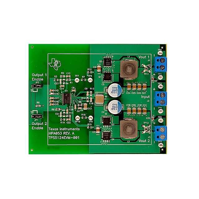
7 PCB Layout
Figure 7-1 through Figure 7-5 shows the PCB layout.
Figure 7-1. Top Assembly
Figure 7-2. Top Side
SLUU182A – JANUARY 2004 – REVISED MARCH 2022
TPS5124 Buck Controller Evaluation Module User's Guide
Submit Document Feedback
Copyright © 2022 Texas Instruments Incorporated
13
�PCB Layout
www.ti.com
Figure 7-3. Internal 1
Figure 7-4. Internal 2
14
TPS5124 Buck Controller Evaluation Module User's Guide
SLUU182A – JANUARY 2004 – REVISED MARCH 2022
Submit Document Feedback
Copyright © 2022 Texas Instruments Incorporated
�www.ti.com
PCB Layout
Figure 7-5. Bottom Side
SLUU182A – JANUARY 2004 – REVISED MARCH 2022
TPS5124 Buck Controller Evaluation Module User's Guide
Submit Document Feedback
Copyright © 2022 Texas Instruments Incorporated
15
�List of Materials
www.ti.com
8 List of Materials
Table 8-1. List of Materials
REFERENCE
DESIGNATOR
QTY
DESCRIPTION
SIZE
MFR
PARTNUMBER
C1–C3
3
Capacitor, ceramic, 2.2 μF, 50 V, X7R, 10%
1210
Std
Std
C12, C22
2
Capacitor, ceramic, 5600 pF, 50 V, X7R,
10%
805
Std
Std
C13
1
Capacitor, ceramic, 10 μF, 10 V, X5R, 10%
1210
Murata
GRM32ER61A106KC01L
C14, C20
2
Capacitor, ceramic, 0.027 μF, 50 V, X7R,
10%
805
Std
Std
C7, C15, C18, C19,
C32
5
Capacitor, ceramic, 0.01 μF, 50 V, X7R, 10% 805
Std
Std
C16
1
Capacitor, ceramic, 47 pF, 50 V, COG, 5%
805
Std
Std
C21, C23
2
Capacitor, ceramic, 1000 pF, 50 V, COG, 5% 805
Std
Std
C24–C31
8
Capacitor, ceramic, 100 μF, 6.3 V, X5R
TDK
C3225X5R0J107M
C4, C5
2
Capacitor, special polymer, 150 μF, 20, 20% 10.3 mm
(F12)
Panasonic
EEFWA1D151P
C6, C8–C11, C17
6
Capacitor, ceramic, 0.1 μF, 50 V, X7R, 10%
805
Std
Std
J1, J2, J3
3
Terminal block, 2 pin, 15 A, 5.1 mm
0.40 × 0.35 OST
JP1, JP2
2
Header, 3-pin, 100-mil spacing (36-pin strip) 0.100 × 3
L1, L2
2
Inductor, SMT, 2.2 μH, 20 A, 4.6 mΩ
0.51 × 0.51 Vishay−Sili IHLP5050EZ−01
conix
Q1, Q3
2
MOSFET, N-channel, 30 V, 18 A, 8.0 mΩ
PWRPAKS Vishay−Sili Si7860DP
0−8
conix
Q2, Q4
2
MOSFET, N-channel, 30 V, 29 A, 3 mΩ
PWRPAKS Vishay−Sili Si7880DP
0−8
conix
R1, R11
2
Resistor, chip, 10.0 kW, 1/10 W, 1%
805
Std
Std
R10
1
Resistor, chip, 68.1 W, 1/10 W, 1%
805
Std
Std
R5
1
Resistor, chip, 10.0 W, 1/10 W, 1%
805
Std
Std
R12, R15
2
Resistor, chip, 1.5 W, 1/10 W, 1%
805
Std
Std
R13
1
Resistor, chip, 20.0 kW, 1/10 W, 1%
805
Std
Std
R14
1
Resistor, chip, 14.0 kW, 1/10 W, 1%
805
Std
Std
R16, R7
2
Resistor, chip, 49.9 W, 1/10 W, 1%
805
Std
Std
R2
1
Resistor, chip, 14 W, 1/10 W, 1%
805
Std
Std
R3
1
Resistor, chip, 3.48 kW, 1/10 W, 1%
805
Std
Std
R4, R8
2
Resistor, chip, 1.10 kW, 1/10 W, 1%
805
Std
Std
R6
1
Resistor, chip, 100 kW, 1/10 W, 1%
805
Std
Std
R9
1
Resistor, chip, 13.0 kW, 1/10 W, 1%
805
Std
Std
TP1–TP10
10
Test point, 0.062 hole
0.25
Keystone
5012
TP11,TP12
2
Adaptor, 3.5-mm probe clip (or
131−5031−00)
0.2
Tektronix
131−4244−00
U1
1
IC, dual-channel synchronous step-down
PWM controller
DBT30
TI
TPS5124DBT
1
PCB, 4 in × 3.2 in × .062 in
Any
HPA053
1210
Sullins
ED1609
PTC36SAAN
9 Revision History
NOTE: Page numbers for previous revisions may differ from page numbers in the current version.
Changes from Revision * (January 2004) to Revision A (March 2022)
Page
• Updated the numbering format for tables, figures, and cross-references throughout the document. ................2
• Updated the user's guide title............................................................................................................................. 2
16
TPS5124 Buck Controller Evaluation Module User's Guide
SLUU182A – JANUARY 2004 – REVISED MARCH 2022
Submit Document Feedback
Copyright © 2022 Texas Instruments Incorporated
�IMPORTANT NOTICE AND DISCLAIMER
TI PROVIDES TECHNICAL AND RELIABILITY DATA (INCLUDING DATA SHEETS), DESIGN RESOURCES (INCLUDING REFERENCE
DESIGNS), APPLICATION OR OTHER DESIGN ADVICE, WEB TOOLS, SAFETY INFORMATION, AND OTHER RESOURCES “AS IS”
AND WITH ALL FAULTS, AND DISCLAIMS ALL WARRANTIES, EXPRESS AND IMPLIED, INCLUDING WITHOUT LIMITATION ANY
IMPLIED WARRANTIES OF MERCHANTABILITY, FITNESS FOR A PARTICULAR PURPOSE OR NON-INFRINGEMENT OF THIRD
PARTY INTELLECTUAL PROPERTY RIGHTS.
These resources are intended for skilled developers designing with TI products. You are solely responsible for (1) selecting the appropriate
TI products for your application, (2) designing, validating and testing your application, and (3) ensuring your application meets applicable
standards, and any other safety, security, regulatory or other requirements.
These resources are subject to change without notice. TI grants you permission to use these resources only for development of an
application that uses the TI products described in the resource. Other reproduction and display of these resources is prohibited. No license
is granted to any other TI intellectual property right or to any third party intellectual property right. TI disclaims responsibility for, and you
will fully indemnify TI and its representatives against, any claims, damages, costs, losses, and liabilities arising out of your use of these
resources.
TI’s products are provided subject to TI’s Terms of Sale or other applicable terms available either on ti.com or provided in conjunction with
such TI products. TI’s provision of these resources does not expand or otherwise alter TI’s applicable warranties or warranty disclaimers for
TI products.
TI objects to and rejects any additional or different terms you may have proposed. IMPORTANT NOTICE
Mailing Address: Texas Instruments, Post Office Box 655303, Dallas, Texas 75265
Copyright © 2022, Texas Instruments Incorporated
�