User's Guide
SLUUBA9A – June 2015 – Revised February 2017
Using the TPS53647: PWR710-EVM, 4-Phase, D-CAP+
Step-Down, DC-DC Analog with PMBus Interface
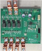
The PWR710-EVM evaluation module (EVM) uses the TPS53647 controller. The controller is 4-phase, DCAP+™ synchronous buck driverless controller with PMBus™ interface. The device operates using a
voltage supply between 4.5 V and 17 V. The controller allows programming and monitoring via the PMBus
interface. This PWR710-EVM uses the CSD95372B, Synchronous Buck NexFET™ Smart Power Stage
(SLPS499) device as the power stage.
1
2
3
4
5
6
7
8
9
10
1
Contents
Description .................................................................................................................... 1
1.1
Typical Applications ................................................................................................ 1
1.2
Features .............................................................................................................. 2
Electrical Performance Specifications ..................................................................................... 2
Schematic ..................................................................................................................... 3
Test Setup .................................................................................................................... 8
4.1
Test and Configuration Software ................................................................................. 8
4.2
Test Equipment ..................................................................................................... 8
4.3
Recommended Test Setup ........................................................................................ 9
4.4
USB Interface Adapter and Cable .............................................................................. 10
4.5
List of Test Points and Connectors ............................................................................. 11
EVM Configuration Using the Fusion GUI .............................................................................. 13
5.1
Configuration Procedure ......................................................................................... 13
Test Procedure ............................................................................................................. 13
6.1
Line/Load Regulation and Efficiency Measurement Procedure ............................................. 13
6.2
Control Loop Gain and Phase Measurement Procedure .................................................... 14
6.3
Efficiency ........................................................................................................... 14
6.4
Equipment Turn-on and Shutdown.............................................................................. 15
Performance Data and Typical Characteristic Curves................................................................. 16
EVM Assembly Drawing and PCB Layout .............................................................................. 19
List of Materials ............................................................................................................. 22
Fusion GUI .................................................................................................................. 24
Description
The PWR710-EVM operates as a single output converter. The nominal 12-V bus produced a regulated,
1.0-V output at up to 120 A of load current. The PWR710-EVM demonstrates the controller in a typical
low-voltage high-current application while providing a number of test points to evaluate the performance of
the controller. Refer to TPS53647 (SLUSC39) datasheet for more information on multi-phase
configuration.
1.1
Typical Applications
•
•
•
•
ASIC power in communications equipment
High density power solutions
Server power
Smart power systems
SLUUBA9A – June 2015 – Revised February 2017
Submit Documentation Feedback
Using the TPS53647: PWR710-EVM, 4-Phase, D-CAP+ Step-Down, DC-DC
Analog with PMBus Interface
Copyright © 2015–2017, Texas Instruments Incorporated
1
�Description
1.2
Features
•
•
•
•
2
www.ti.com
Regulated 1.0-V output up to 120-A DC steady state output current
Output can be marginable and trimmable via the PMBus interface
Programmable through PMBus interface
– UVLO protection threshold
– Soft-start slew-rate
– Device enable and disable
– Overcurrent warning and fault limits
– SW frequency
– BOOT voltage
Convenient test points for probing critical waveforms
Electrical Performance Specifications
Table 1. PWR710-EVM Electrical Performance Specifications
PARAMETER
TEST CONDITIONS
MIN
TYP
MAX
8
12
14
UNITS
INPUT CHARACTERISTICS
VIN
Voltage range
V
IIN(max)
Maximum input current
VIN = 8 V, IOUT = 120 A
17
A
No load input current
VIN = 14 V, IOUT = 0 A
120
mA
OUTPUT CHARACTERISTICS
VOUT
Output voltage
IOUT
Output load current
VRIPPLE
1.0
0
Output voltage line regulation
8 V ≤ VIN ≤ 14 V
0.03%
Output voltage load regulation
0 A ≤ IOUT ≤ 120 A
0.03%
Output voltage ripple
VIN = 12 V, IOUT = 120 A
Output overcurrent protection
(OCP)
V
120
A
3.8
mVpp
150
A
500
kHz
SYSTEMS CHARACTERISTICS
fSW
TJ
2
Switching frequency
VIN = 12 V
Peak efficiency
VIN = 12 V, IOUT = 74 A
91%
Full-load efficiency
VIN = 12 V, IOUT = 120 A
90%
Operating temperature
25
Using the TPS53647: PWR710-EVM, 4-Phase, D-CAP+ Step-Down, DC-DC
Analog with PMBus Interface
ºC
SLUUBA9A – June 2015 – Revised February 2017
Submit Documentation Feedback
Copyright © 2015–2017, Texas Instruments Incorporated
�Schematic
www.ti.com
3
Schematic
TP1
Vin: 8-14Vdc
J1
L1
VIN
VIN
VIN_C
TP3
IMON
IMON
J2
J3
1
3
SKIP#_NVM
R2 150k
2
4
C2
22µF
GND
R1
49.9k
C3
2200pF
C1
22µF
TP2
NVM
R3 20.0k
Pinstraps
VIN_C
C4
22µF
TP4
TSEN
R4
TAO
TSEN
C12
270µF
0
R5
121k
C5
22µF
C6
22µF
C7
22µF
C8
22µF
C9
22µF
C10
3300pF
C11
3300pF
C13
270µF
C20
1000pF
C15
22µF
C14
22µF
C16
22µF
C17
22µF
C18
22µF
C19
22µF
C21
3300pF
3300pF
C22
TP5
AGND
C26
1µF
C23
1µF
C25
4.7µF
U1
1_8V_LDO
TP6
V3R3
5V_CON
R6 1.00
VIN_C
V3R3
R8
2.00k
TP10
ENABLE
RESET#
J5
C29
1µF
VSP
VSN
VREF
R15
33.2k
R10
26.7k
R11
9.31k
5V_CON
V12
V3R3
ENABLE
RESET#
PMB_CLK
PMB_ALERT#
PMB_DIO
TSEN
R14
4.32k
C24
0.33µF TP7
TP8
5V_CON
R13
16.5k
R12
16.5k
ADDR_TRISE
SLEW-MODE
O-USR
VBOOT
F-IMAX
OCP-R
CSP1
CSP2
CSP3
CSP4
15
16
14
23
21
PMB_CLK
PMB_ALERT#
PMB_DIO
24
25
26
TSEN
40
VSP
VSN
9
10
CSP1
CSP2
CSP3
CSP4
3
4
5
6
ADDR_TRISE
SLEW-MODE
O-USR
VBOOT
F-IMAX
28
29
30
31
32
OCP-R
1
TPS53647RHA
V5
V12
V3R3
VREF
ISUM
ENABLE
IMON
RESET
COMP
PMB_CLK
PMB_ALERT
PMB_DIO
PWM1
PWM2
PWM3
PWM4
J4
13
VREF
VREF
12
ISUM
ISUM TP9
2
IMON
11
COMP
38
37
36
35
PWM1
PWM2
PWM3
PWM4
1
3
5
7
9
VREF
R7
2.55k
IMON
TP11
COMP
2
4
6
8
10
PMB_ALERT#
PMB_DIO
C27
R9
PMB_CLK
8.06k
PWM1
PWM2
PWM3
PWM4
1000pF
C28
J6
12pF
1_8V_LDO
TSEN
VSP
VSN
VR_RDY
VR_FAULT
VR_HOT
CSP1
CSP2
CSP3
CSP4
SKIP_NVM
ADDR_TRISE
SLEW-MODE
O-USR
VBOOT
F-IMAX
OCP-R
NC
NC
NC
NC
GND
GND
GND
PAD
18
27
19
VR_RDY
VR_FAULT#
VR_HOT#
39
SKIP#_NVM
VR_RDY
1
2
3
3_3V_LDO
VR_FAULT#
VR_HOT#
SKIP#_NVM
7
8
33
34
R17
10.0k
TP12
PMB_CLK
17
20
22
41
R16
10.0k
R18
10.0k
C30
0.1µF
P_CLK
TP13
PMB_ALERT#
P_ALERT#
TP14
V3R3
P_DIO
PMB_DIO
R20
20.0k
R27
30.1k
R24
39.2k
R25
150k
R19
24.3k
R21
24.3k
AGND
R28
PWRGND
R26
10.0k
R23
10.0k
R22
10.0k
0
TP16
TP15
VR_RDY
AGND
PWRGND
VR_RDY
TP17
VR_FAULT#
VR_FAULT#
VR_HOT#
VR_HOT#
Figure 1. PWR710-EVM Schematic Controller
SLUUBA9A – June 2015 – Revised February 2017
Submit Documentation Feedback
Using the TPS53647: PWR710-EVM, 4-Phase, D-CAP+ Step-Down, DC-DC
Analog with PMBus Interface
Copyright © 2015–2017, Texas Instruments Incorporated
3
�Schematic
www.ti.com
U2
C31
TP18
7
VIN_C
PWM1
12
PWM1
R39
SKIP#_NVM
10
VIN
PWM
5
1.00
R31
3
V3R3
VDD
R35
CSP1
1
0
ENABLE
REFIN
2
IOUT
PGND
PGND
4
13
VREF
C47
0.1µF
CSD95372BQ5M
C35
1000pF
R37
DNP
C41
DNP
VOUT
L2
6
VSW
10.0k
C33 2.2µF
C37
1000pF
11
TAO/FAULT
R29
TAO
0.1µF
R33 0
8
BOOT_R
FCCM
0
5V_DRV
9
BOOT
C43
DNP
C39
1000pF
C44
470µF
R43
1.00
VREF
Figure 2. Phase 1
U5
C50
TP21
7
VIN_C
PWM4
12
PWM4
R56
10
SKIP#_NVM
VIN
BOOT
PWM
BOOT_R
FCCM
0
TAO/FAULT
R46
5V_DRV
1.00
R48
V3R3
5
VDD
3
C52 2.2µF
R52
1
TAO
0.1µF
R50 0
8
C56
1000pF
VOUT
11
VSW
6
ENABLE
REFIN
2
IOUT
PGND
PGND
4
13
10.0k
CSP4
9
L5
VREF
C64
0.1µF
C58
1000pF
0
C60
DNP
CSD95372BQ5M
C54
1000pF
R54
DNP
R60
1.00
VREF
Figure 3. Phase 2
U4
TP20
C49
7
VIN_C
PWM3
12
PWM3
R55
10
SKIP#_NVM
VIN
BOOT
PWM
BOOT_R
FCCM
0
5V_DRV
TAO/FAULT
R45
1.00
R47
V3R3
5
VDD
3
R51
CSP3
1
TAO
0.1µF
R49 0
8
C55
1000pF
VOUT
11
VSW
6
ENABLE
REFIN
2
IOUT
PGND
PGND
4
13
10.0k
C51 2.2µF
9
L4
PA2607.151NLT
VREF
C63
0.1µF
C57
1000pF
C61
470µF
C62
DNP
0
C59
DNP
R53
DNP
CSD95372BQ5M
C53
1000pF
R59
1.00
VREF
Figure 4. Phase 3
4
Using the TPS53647: PWR710-EVM, 4-Phase, D-CAP+ Step-Down, DC-DC
Analog with PMBus Interface
SLUUBA9A – June 2015 – Revised February 2017
Submit Documentation Feedback
Copyright © 2015–2017, Texas Instruments Incorporated
�Schematic
www.ti.com
U5
C50
TP21
7
VIN_C
PWM4
12
PWM4
R56
10
SKIP#_NVM
VIN
PWM
BOOT_R
FCCM
0
5V_DRV
TAO/FAULT
R46
1.00
BOOT
R48
V3R3
5
VDD
3
C52 2.2µF
R52
1
8
TAO
0.1µF
R50 0
C56
1000pF
VOUT
11
VSW
6
ENABLE
REFIN
2
IOUT
PGND
PGND
4
13
10.0k
CSP4
9
L5
VREF
C64
0.1µF
C58
1000pF
0
C60
DNP
CSD95372BQ5M
C54
1000pF
R54
DNP
R60
1.00
VREF
Figure 5. Phase 4
SLUUBA9A – June 2015 – Revised February 2017
Submit Documentation Feedback
Using the TPS53647: PWR710-EVM, 4-Phase, D-CAP+ Step-Down, DC-DC
Analog with PMBus Interface
Copyright © 2015–2017, Texas Instruments Incorporated
5
�6
Using the TPS53647: PWR710-EVM, 4-Phase, D-CAP+ Step-Down, DC-DC
Analog with PMBus Interface
Copyright © 2015–2017, Texas Instruments Incorporated
PWRGND
C81
DNP
C67
DNP
C82
100µF
C68
100µF
C83
100µF
C69
100µF
C80
100µF
CSP4
TP25
CSP3
TP24
CSP2
TP23
CSP1
TP22
C70
100µF
CSP4
CSP3
CSP2
C84
100µF
DNP
R70
DNP
R65
DNP
R62
DNP
R61
CSP1
C65
100µF
C85
100µF
C71
100µF
Disable Phase 4
when R70 = 0
C86
100µF
Disable Phase 3 4
when R65 = 0
Disable Phase 2 3 4
when R62 = 0
Disable Phase 1 2 3 4
when R61= 0
V3R3
C72
100µF
C87
100µF
C66
DNP
C88
DNP
C73
100µF
J7
C89
DNP
C74
100µF
C90
DNP
PWRGND
R69
0
R63
0
C75
100µF
0
R66
0
R64
VOUT
C91
DNP
R67
DNP
C76
100µF
C92
DNP
AGND
R68
DNP
J8
C77
100µF
C93
DNP
VSN
VSP
C78
100µF
VSN
VSP
C94
DNP
C79
100µF
J9
VOUT
GND
TP27
VOUT
TP26
Vout: 1.0Vdc
Iout: 120A
J13
J12
J11
J10
Schematic
www.ti.com
Figure 6. Output Filter
SLUUBA9A – June 2015 – Revised February 2017
Submit Documentation Feedback
�ENABLE
5VIN
SLUUBA9A – June 2015 – Revised February 2017
Submit Documentation Feedback
0
R41
ENABLE
TP28
R71
1.00k
C97
0.1µF
C95
0.01µF
3
1
R74
100k
C98
10µF
3_3V_LDO
PGD_1
EG1218
S1
Copyright © 2015–2017, Texas Instruments Incorporated
1
11
20
6
7
9
10
2
3
1-2 OFF
2-3 ON
EP
GND
RESET
MR1
MR2
PG1
FB2
VOUT2
VOUT2
FB1
VOUT1
VOUT1
TPS70102PWP
NC
NC
NC
EN
SEQ
VIN2
VIN2
VIN1
VIN1
U6
2
21
8
15
4
5
16
14
12
13
17
18
19
J14
GND
TP30
5VIN
PGD_1
5VIN
R58
51.1k
R75
15.0k
30.1k
R57
R42
30.1k
5VIN
TP29
5V_CON
C99
10µF
3_3V_LDO
TP32
1_8V_LDO
TP31
R73
1.0
C96
10µF
R76
2.00k
5V_DRV
R72
1.0
RESET
3_3V_LDO
1_8V_LDO
www.ti.com
Schematic
Figure 7. Auxiliary Circuitry
Using the TPS53647: PWR710-EVM, 4-Phase, D-CAP+ Step-Down, DC-DC
Analog with PMBus Interface
7
�Test Setup
www.ti.com
4
Test Setup
4.1
Test and Configuration Software
Use the TI Fusion Digital Power Designer software to change any of the default configuration parameters
on the EVM. To download this software, visit the Digital Power Software page.
4.1.1
Description
Fusion Digital Power Designer is the graphic user interface (GUI) used to configure and monitor controller
on the EVM. The software uses the PMBus protocol to communicate with the controller over serial bus by
way of a TI USB adapter (see Figure 9).
4.1.2
TI Fusion Digital Power Designer Features
The software offers these features:
• Turn on or off the power supply output, either through the hardware control line or the PMBus
operation command.
• Monitor real-time data. Items such as input voltage, output voltage, output current, temperature,
warnings and faults are continuously monitored and displayed by the GUI.
• Configure common operating characteristics such as output voltage trim and margin, VIN UVLO, softstart slew rate, switching frequency, and warning and fault thresholds.
4.2
4.2.1
Test Equipment
Voltage Sources
Two DC input voltage sources are needed (VIN and 5VIN). Use an input voltage source VIN between 0 V
and 14 V variable DC source capable of supplying 20 Adc. Use another input voltage source 5VIN a 5-V
DC source capable of supplying 1Adc. Connect VIN to J1, J2 and connect 5VIN to J14 as shown in
Figure 8.
4.2.2
Multimeters
It is recommended to use two separate multimeters as shown in Figure 8. One meter is to measure VIN,
the other one is to measure VOUT.
4.2.3
Output Load
The electronic load is recommended for the test setup as shown in Figure 8. The load should be capable
of 120 A.
4.2.4
Oscilloscope
Use an oscilloscope to measure output noise and ripple. Use a coaxial cable to measure output ripple
across the output ceramic capacitor, C76.
4.2.5
Fan
During prolonged operation at high load, it may be necessary to provide forced air cooling with a small fan
aimed at the EVM. Maintain the temperature of the devices on the EVM under 105°C.
4.2.6
USB-to-GPIO Interface Adapter
A communications adapter is required between the EVM and the host computer. This EVM is designed to
use the Texas Instruments USB-to-GPIO adapter, see Figure 9. To purchase this adapter visit the TI usbto-gpio tool page.
4.2.7
8
Recommended Wire Gauge
Using the TPS53647: PWR710-EVM, 4-Phase, D-CAP+ Step-Down, DC-DC
Analog with PMBus Interface
SLUUBA9A – June 2015 – Revised February 2017
Submit Documentation Feedback
Copyright © 2015–2017, Texas Instruments Incorporated
�Test Setup
www.ti.com
Table 2. Recommended Wire Gauge
Voltage (V)
(1)
4.3
CONNECT
RECOMMENDED
WIRE SIZE
12
VIN to J1
AWG #10
5
5VIN to J14
AWG #18
1
Load to J10 and J11
4 × AWG #10
MAXIMUM TOTAL WIRE LENGTH
(FEET)
RETURN
2
(1)
INPUT
OUTPUT
2
n/a
2
n/a
n/a
2
Total length of wire less than 4 feet (2 feet input or output, 2 feet return).
Recommended Test Setup
Figure 8 shows the recommended test setup, which includes VIN and 5VIN input voltage sources, output
load, and USB-to-GPIO adapter.
Figure 8. PWR710-EVM Recommended Test Setup
SLUUBA9A – June 2015 – Revised February 2017
Submit Documentation Feedback
Using the TPS53647: PWR710-EVM, 4-Phase, D-CAP+ Step-Down, DC-DC
Analog with PMBus Interface
Copyright © 2015–2017, Texas Instruments Incorporated
9
�Test Setup
4.4
www.ti.com
USB Interface Adapter and Cable
Figure 9 shows the USB interface adapter and cable.
Figure 9. Texas Instruments USB-to-GPIO Adapter and Connections
10
Using the TPS53647: PWR710-EVM, 4-Phase, D-CAP+ Step-Down, DC-DC
Analog with PMBus Interface
SLUUBA9A – June 2015 – Revised February 2017
Submit Documentation Feedback
Copyright © 2015–2017, Texas Instruments Incorporated
�Test Setup
www.ti.com
4.5
List of Test Points and Connectors
Table 3 lists the test point functions.
Table 3. Test Point Functions
TEST POINT
NAME
DESCRIPTION
TP1
VIN
VIN+ measurement point
TP2
GND
VIN– measurement point
TP3
IMON
IMON signal
TP4
TSEN
TSEN signal
TP5
AGND
Analog Ground
TP6
V3R3
Internal 3.3-V LDO output measurement point
TP7
VREF
Internal reference voltage measurement point
TP8
5V_CON
5-V controller power input measurement point
TP9
ISUM
ISUM signal
TP10
RESET#
RESET signal
TP11
COMP
COMP signal
TP12
P_CLK
PMBus clock signal
TP13
P_ALERT#
PMBus alert signal
TP14
P_DIO
PMBus digital I/O signal
TP15
VR_RDY
VR_RDY signal
TP16
VR_FAULT#
VR_FAULT signal
TP17
VR_HOT#
VR_HOT signal
TP18
PWM1
PWM signal of Phase 1
TP19
PWM2
PWM signal of Phase 2
TP20
PWM3
PWM signal of Phase 3
TP21
PWM4
PWM signal of Phase 4
TP22
CSP1
Current sense signal of Phase 1
TP23
CSP2
Current sense signal of Phase 2
TP24
CSP3
Current sense signal of Phase 3
TP25
CSP4
Current sense signal of Phase 4
TP26
VOUT
VOUT+ measurement point
TP27
GND
VOUT– measurement point
TP28
ENABLE
ENABLE signal
TP29
5VIN
5VIN+ measurement point
TP30
GND
5VIN– measurement point
TP31
1_8V_LDO
1.8-V external LDO output measurement point
TP32
3_3V_LDO
3.3-V external LDO output measurement point
Table 4 lists the EVM connector functions.
Table 4. Connector Functions
Connector
TYPE
DESCRIPTION
J1
CB35-36-CY
VIN+ connector
J2
CB35-36-CY
VIN– connector
J3
TSW-102-07G-D
Choose NVM or pin strap
J4
TSW-105-07G-D
PMBus connector
J5
TSW-102-07G-S
Reset
SLUUBA9A – June 2015 – Revised February 2017
Submit Documentation Feedback
Using the TPS53647: PWR710-EVM, 4-Phase, D-CAP+ Step-Down, DC-DC
Analog with PMBus Interface
Copyright © 2015–2017, Texas Instruments Incorporated
11
�Test Setup
www.ti.com
Table 4. Connector Functions (continued)
12
Connector
TYPE
DESCRIPTION
J6
TSW-103-07G-S
Choose PMBus pull up voltage(1.8V or 3.3V)
J7
TSW-102-07G-S
VOUT connector for bode plot measurement
J8
TSW-102-07G-S
VOUT connector for bode plot measurement
J9
TSW-102-07G-S
VOUT measurement connector
J10
CB35-36-CY
VOUT+ connector
J11
CB35-36-CY
VOUT+ connector
J12
CB35-36-CY
VOUT- connector
J13
CB35-36-CY
VOUT- connector
J14
ED555/2DS
5VIN connector
Using the TPS53647: PWR710-EVM, 4-Phase, D-CAP+ Step-Down, DC-DC
Analog with PMBus Interface
SLUUBA9A – June 2015 – Revised February 2017
Submit Documentation Feedback
Copyright © 2015–2017, Texas Instruments Incorporated
�EVM Configuration Using the Fusion GUI
www.ti.com
5
EVM Configuration Using the Fusion GUI
The controller on this EVM leaves the factory pre-configured. Table 5 lists some key factory configuration
parameters from the configuration file.
Table 5. Key Factory Configuration Parameters
CMD NAME
CMDCODEHEX
ENCODEDHEX
DECODED
COMMENTS
VIN UVLO
0xE0
0x01
7.25 V
Input voltage turn on threshold
IOUT_OC_FAULT_LIMIT
0x46
0x0096
150.00 A
OC fault level
IOUT_OC_WARN_LIMIT
0x4A
0x0078
120.0 A
OC warning level
ON_OFF_CONFIG
0x02
0x17
Control Pin only
Power is converted when the control
pin is active
OT_FAULT_LIMIT
0x4F
0x007D
125 °C
OT fault level
OT_WARN_LIMIT
0x51
0x005F
95 °C
OT warn level
Max Num Phases
0xE4
0x03
4 Phase
phase numbers
SWITCHING FREQUENCY
0xDC
0x20
500kHz
switching frequency
VBOOT
0xDB
0x97
1.000V
VBOOT voltage
To configure the EVM with other than the factory settings shown in Table 5, use the TI Fusion Digital
Power Designer software for reconfiguration. Be sure to apply the 5VIN input voltage to the EVM prior to
launching the software. This sequence ensures that the controller and GUI recognize each other.
5.1
Configuration Procedure
1. Adjust the input supply 5VIN to provide 5 VDC, current limited to 1 A.
2. Apply the input power source VIN to the EVM. Refer to Figure 8 and Figure 9 for connections and test
setup.
3. Launch the Fusion GUI software. Refer to the screenshots in Section 10 for more information.
4. Configure the EVM operating parameters as desired.
6
Test Procedure
6.1
Line/Load Regulation and Efficiency Measurement Procedure
1. Set up EVM as described in Figure 8.
2. Ensure the electronic load is set to draw 0 Adc.
3. Increase 5VIN from 0 V to 5 V.
4. Increase VIN from 0 V to 12 V.
5. Put switch S1 to ON position.
6. Turn on the external fan if necessary.
7. Vary the load from 0 Adc to 120 Adc. Ensure VOUT remains in regulation as defined in Table 1.
8. Vary VIN from 8 V to 14 V. Ensure VOUT remains in regulation as defined in Table 1.
9. Decrease the load to 0 A.
10. Put switch S1 to OFF position.
11. Decrease VIN to 0 V.
12. Decrease 5VIN to 0 V.
13. Shut down the external fan if in use.
SLUUBA9A – June 2015 – Revised February 2017
Submit Documentation Feedback
Using the TPS53647: PWR710-EVM, 4-Phase, D-CAP+ Step-Down, DC-DC
Analog with PMBus Interface
Copyright © 2015–2017, Texas Instruments Incorporated
13
�Test Procedure
6.2
www.ti.com
Control Loop Gain and Phase Measurement Procedure
The PWR710 EVM includes a 0-Ω series resistor R64 in the feedback loop. This resistor value can be
changed to 10 Ω and then be used for loop response analysis, which is accessible at the connector J7
and J8. These two connectors should be used during loop response measurements as the injection points
for the loop perturbation. See short description below in Table 6.
Table 6. Test Points for Loop Response Measurements
TEST POINT
6.2.1
1.
2.
3.
4.
5.
6.
7.
6.3
NODE
DESCRIPTION
COMMENT
J8+
INPUT
Input to feedback of VOUT
The amplitude of the perturbation at this
node should be limited to less than 100 mV.
J7+
OUTPUT
Resulting output of VOUT
Bode can be measured by a network
analyzer as J7+ / J8+.
Procedure
Set up EVM as described in Figure 8.
Connect the network analyzer isolation transformer from J8+ to J7+.
Connect the input signal measurement probe to J8+.
Connect output signal measurement probe to J7+.
Connect the ground leads of both probe channels to J7– or J8–.
On the network analyzer, measure the Bode as J7+ / J8+ (Out / In).
Disconnect the isolation transformer from the bode plot test points and change the resistor R64 back to
0 Ω before making other measurements, because the signal injection into the feedback loop may
interfere with the accuracy of other measurements.
Efficiency
In order to measure the efficiency of the power train on the EVM, it is important to measure the voltages at
the correct location. This is necessary because otherwise the measurements will include losses that are
not related to the power train itself. Losses incurred by the voltage drop in the copper traces and in the
input and output connectors are not related to the efficiency of the power train, and they should not be
included in efficiency measurements.
Input current can be measured at any point in the input wires, and output current can be measured
anywhere in the output wires of the output being measured.
Figure 10 shows the measurement points for input voltage and output voltage. Using these measurement
points results in efficiency measurements that do not include losses due to the connectors and PCB
traces.
14
Using the TPS53647: PWR710-EVM, 4-Phase, D-CAP+ Step-Down, DC-DC
Analog with PMBus Interface
SLUUBA9A – June 2015 – Revised February 2017
Submit Documentation Feedback
Copyright © 2015–2017, Texas Instruments Incorporated
�Test Procedure
www.ti.com
Figure 10. Test Setup for Efficiency Measurement
6.4
Equipment Turn-on and Shutdown
6.4.1
1.
2.
3.
4.
5.
Turn-on Sequence
Turn on input power supply 5VIN.
Turn on input power supply VIN and increase VIN above 8 V.
Switch S1 to ‘ON’ position.
Adjust load current as desired.
Turn on the external fan if necessary.
1.
2.
3.
4.
5.
Shutdown Sequence
Reduce the load current to 0 A.
Switch S1 to ‘OFF’ position.
Reduce input voltage to 0 V and shut down input power supply VIN.
Shut down input power supply 5VIN.
Shut down the external FAN if in use.
6.4.2
SLUUBA9A – June 2015 – Revised February 2017
Submit Documentation Feedback
Using the TPS53647: PWR710-EVM, 4-Phase, D-CAP+ Step-Down, DC-DC
Analog with PMBus Interface
Copyright © 2015–2017, Texas Instruments Incorporated
15
�Performance Data and Typical Characteristic Curves
7
www.ti.com
Performance Data and Typical Characteristic Curves
Figure 11 through Figure 13 show the typical performance curves for the PWR710-EVM.
1
100
VIN = 8 V
VIN = 12 V
VIN = 14 V
95
0.99975
Output Voltage (V)
90
Efficiency (%)
85
80
75
70
0.9995
0.99925
0.999
65
0.99875
VIN = 8 V
VIN = 12 V
VIN = 14 V
55
0.9985
0
50
0
10
20
30
40 50 60 70 80
Output Current (A)
10
20
90 100 110 120
40 50 60 70 80
Output Current (A)
D001
Figure 12. Load Regulation (VOUT = 1.0 V)
100
80
200
Gain
Phase 160
60
120
40
80
20
40
0
0
-20
-40
-40
-80
-60
-120
-80
-160
-100
1000
90 100 110 120
D001
Figure 11. Efficiency of Output vs Line and Load (VOUT =
1.0 V)
Gain (dB)
30
Phase (°)
60
-200
1000000
10000
100000
Frequency (Hz)
D002
D008
D001
Figure 13. Bode Plot (VIN= 12 V, VOUT = 1.0 V, IOUT = 120A)
16
Using the TPS53647: PWR710-EVM, 4-Phase, D-CAP+ Step-Down, DC-DC
Analog with PMBus Interface
SLUUBA9A – June 2015 – Revised February 2017
Submit Documentation Feedback
Copyright © 2015–2017, Texas Instruments Incorporated
�Performance Data and Typical Characteristic Curves
www.ti.com
Figure 14 through Figure 19 show the waveforms for the PWR710-EVM.
VIN = 12 V, VOUT = 1.0 V
VIN = 12 V, VOUT = 1.0 V
Figure 14. Transient Response (Load Step 0 A to 40 A,
5A/us Slew Rate)
VIN = 12 V, VOUT = 1.0 V
Figure 15. Transient Response (Load Step 40 A to 0 A,
5A/us Slew Rate)
VIN = 12 V, VOUT = 1.0 V, IOUT = 120 A
Figure 16. Transient Response (Load Step 0 A to 40 A to
0A, 5A/us Slew Rate)
SLUUBA9A – June 2015 – Revised February 2017
Submit Documentation Feedback
Figure 17. Output Ripple
Using the TPS53647: PWR710-EVM, 4-Phase, D-CAP+ Step-Down, DC-DC
Analog with PMBus Interface
Copyright © 2015–2017, Texas Instruments Incorporated
17
�Performance Data and Typical Characteristic Curves
VIN = 12 V, VOUT = 1.0 V, IOUT = 0 A
www.ti.com
VIN = 12 V, VOUT = 1 V, IOUT = 6 A
Figure 18. Enable Startup
18
Using the TPS53647: PWR710-EVM, 4-Phase, D-CAP+ Step-Down, DC-DC
Analog with PMBus Interface
Figure 19. Enable Shutdown
SLUUBA9A – June 2015 – Revised February 2017
Submit Documentation Feedback
Copyright © 2015–2017, Texas Instruments Incorporated
�EVM Assembly Drawing and PCB Layout
www.ti.com
8
EVM Assembly Drawing and PCB Layout
Figure 20 through Figure 29 show the design of the PWR710 EVM printed circuit board.
Figure 20. Top Layer Assembly Drawing (Top View)
Figure 21. Bottom Layer Assembly Drawing (Bottom View)
Figure 22. Top Copper (Top View)
Figure 23. Internal Layer 1 (Top View)
SLUUBA9A – June 2015 – Revised February 2017
Submit Documentation Feedback
Using the TPS53647: PWR710-EVM, 4-Phase, D-CAP+ Step-Down, DC-DC
Analog with PMBus Interface
Copyright © 2015–2017, Texas Instruments Incorporated
19
�EVM Assembly Drawing and PCB Layout
20
www.ti.com
Figure 24. Internal Layer 2 (Top View)
Figure 25. Internal Layer 3 (Top View)
Figure 26. Internal Layer 4 (Top View)
Figure 27. Internal Layer 5 (Top View)
Using the TPS53647: PWR710-EVM, 4-Phase, D-CAP+ Step-Down, DC-DC
Analog with PMBus Interface
SLUUBA9A – June 2015 – Revised February 2017
Submit Documentation Feedback
Copyright © 2015–2017, Texas Instruments Incorporated
�EVM Assembly Drawing and PCB Layout
www.ti.com
Figure 28. Internal Layer 6 (Top View)
SLUUBA9A – June 2015 – Revised February 2017
Submit Documentation Feedback
Figure 29. Bottom Copper (Top View)
Using the TPS53647: PWR710-EVM, 4-Phase, D-CAP+ Step-Down, DC-DC
Analog with PMBus Interface
Copyright © 2015–2017, Texas Instruments Incorporated
21
�List of Materials
9
www.ti.com
List of Materials
Table 7. List of Materials
QTY (1)
(1)
22
REF DES
DESCRIPTION
PART NUMBER
MANUF
1
PCB
Printed Circuit Board
PWR710
Any
14
C1, C2, C4, C5,
C6, C7, C8, C9,
C14, C15, C16,
C17, C18, C19
Capacitor, ceramic 22 µF, 25 V, ±20%, X5R,
1206_190
C3216X5R1E226M160AB
TDK
1
C3
Capacitor, ceramic 2200 pF, 50 V, ±10%, X7R,
0603
C0603C222K5RAC
Kemet
4
C10, C11, C21,
C22
Capacitor, ceramic 3300 pF, 50 V, ±10%, X7R,
0402
C1005X7R1H332K
TDK
2
C12, C13
Capacitor, aluminum, 270 µF, 16 V, ±20%, 0.01
Ω, TH
16SEPC270MX
Panasonic
1
C20
Capacitor, ceramic 1000 pF, 16 V, ±10%, X7R,
0603
GRM188R71C102KA01D
MuRata
2
C23, C29
Capacitor, ceramic 1 µF, 10 V, ±10%, X7R, 0603 GRM188R71A105KA61D
MuRata
1
C24
Capacitor, ceramic 0.33 µF, 10 V, ±10%, X7R,
0603
GRM188R71A334KA61D
MuRata
1
C25
Capacitor, ceramic 4.7 µF, 16 V, ±10%, X5R,
0603
GRM188R61C475KAAJ
MuRata
1
C26
Capacitor, ceramic 1 µF, 25 V, ±10%, X7R, 0603 GRM188R71E105KA12D
MuRata
1
C27
Capacitor, ceramic 1000 pF, 25 V, ±5%,
C0G/NP0, 0603
GRM1885C1E102JA01D
MuRata
1
C28
Capacitor, ceramic 12 pF, 50 V, ±5%, C0G/NP0,
0603
GRM1885C1H120JA01D
MuRata
10
C30, C31, C32,
C47, C48, C49,
C50, C63, C64,
C97
Capacitor, ceramic 0.1 µF, 25 V, ±10%, X7R,
0603
GRM188R71E104KA01D
MuRata
4
C33, C34, C51,
C52
Capacitor, ceramic 2.2 µF, 10 V, ±10%, X7R,
0603
GRM188R71A225KE15D
MuRata
8
C35, C36, C37,
C38, C53, C54,
C55, C56
Capacitor, ceramic 1000 pF, 25 V, ±10%, X7R,
0603
GRM188R71E102KA01D
MuRata
4
C39, C40, C57,
C58
Capacitor, ceramic 1000 pF, 50 V, ±10%, X7R,
0402
GRM155R71H102KA01D
MuRata
4
C44, C45, C46,
C61
Capacitor, aluminum polymer, 470 µF, 2.5 V,
±20%, 0.003 Ω, SMD 7.3 x 1.9 x 4.3mm SMD
EEF-GX0E471R
Panasonic
20
C65,
C70,
C73,
C76,
C79,
C83,
C86,
Capacitor, ceramic 100 µF, 4 V, ±20%, X5R,
1206
GRM31CR60G107ME39L
MuRata
1
C95
Capacitor, ceramic 0.01 µF, 25 V, ±10%, X7R,
0603
GRM188R71E103KA01D
MuRata
3
C96, C98, C99
Capacitor, ceramic 10 µF, 10 V, ±20%, X5R,
0805
GRM219R61A106ME47
MuRata
6
H1, H2, H3, H4,
H5, H6
Machine screw nut, Hex, 3/8', Stn, Steel, 10-32
HNSS 102
6
H7, H8, H9, H10,
H11, H12
Machine screw pan Slotted 10-32
PMS 102 0050 SL
B&F Fastener
Supply
6
H13, H14, H15,
H16, H17, H18
Washer, split lock, #10
1477
Keystone
6
J1, J2, J10, J11,
J12, J13
Terminal, 50-A Lug
CB35-36-CY
Panduit
C68,
C71,
C74,
C77,
C80,
C84,
C87
C69,
C72,
C75,
C78,
C82,
C85,
component of quantity 0 indicates not populated.
Using the TPS53647: PWR710-EVM, 4-Phase, D-CAP+ Step-Down, DC-DC
Analog with PMBus Interface
SLUUBA9A – June 2015 – Revised February 2017
Submit Documentation Feedback
Copyright © 2015–2017, Texas Instruments Incorporated
�List of Materials
www.ti.com
Table 7. List of Materials (continued)
QTY
(1)
REF DES
DESCRIPTION
PART NUMBER
MANUF
1
J3
Header, 100 mil, 2 x 2, Gold, TH
TSW-102-07-G-D
Samtec
1
J4
Header, 100 mil, 5 x 2, Gold, TH
TSW-105-07-G-D
Samtec
4
J5, J7, J8, J9
Header, 100 mil, 2 x 1, Gold, TH
TSW-102-07-G-S
Samtec
1
J6
Header, 100mil, 3 x 1, Gold, TH
TSW-103-07-G-S
Samtec
1
J14
Terminal block, 6 A, 3.5-mm Pitch, 2-Pos, TH
ED555/2DS
On-Shore
Technology
1
L1
Inductor, 65 nH, 24 A, 0.00032 ohm, SMD
59PR65-650
Vitec Corporation
4
L2, L3, L4, L5
Inductor, Ferrite, 150 nH, 41 A, 0.00029 ohm,
SMD
PA2607.151NLT
Pulse Engineering
1
R1
RES, 49.9 kΩ, 1%, 0.1 W, 0603
CRCW060349K9FKEA
Vishay-Dale
2
R2, R25
RES, 150 kΩ, 1%, 0.1 W, 0603
CRCW0603150KFKEA
Vishay-Dale
2
R3, R20
RES, 20.0 kΩ, 1%, 0.1 W, 0603
CRCW060320K0FKEA
Vishay-Dale
19
R4, R28, R33,
R34, R35, R36,
R39, R40, R41,
R49, R50, R51,
R52, R55, R56,
R63, R64, R66,
R69
Resistor, 0 Ω, 5%, 0.1 W, 0603
MCR03EZPJ000
Rohm
1
R5
Resistor, 121 kΩ, 1%, 0.1 W, 0603
CRCW0603121KFKEA
Vishay-Dale
9
R6, R29, R30,
R43, R44, R45,
R46, R59, R60
Resistor, 1.00 Ω, 1%, 0.1 W, 0603
CRCW06031R00FKEA
Vishay-Dale
1
R7
Resistor, 2.55 kΩ, 1%, 0.1 W, 0603
CRCW06032K55FKEA
Vishay-Dale
2
R8, R76
Resistor, 2.00 kΩ, 1%, 0.1 W, 0603
CRCW06032K00FKEA
Vishay-Dale
1
R9
Resistor, 8.06 kΩ, 1%, 0.1 W, 0603
CRCW06038K06FKEA
Vishay-Dale
1
R10
Resistor, 26.7 kΩ, 1%, 0.1 W, 0603
CRCW060326K7FKEA
Vishay-Dale
1
R11
Resistor, 9.31 kΩ, 1%, 0.1 W, 0603
CRCW06039K31FKEA
Vishay-Dale
2
R12, R13
Resistor, 16.5 kΩ, 1%, 0.1 W, 0603
CRCW060316K5FKEA
Vishay-Dale
1
R14
Resistor, 4.32 kΩ, 1%, 0.1 W, 0603
CRCW06034K32FKEA
Vishay-Dale
1
R15
Resistor, 33.2 kΩ, 1%, 0.1 W, 0603
CRCW060333K2FKEA
Vishay-Dale
10
R16, R17, R18,
R22, R23, R26,
R31, R32, R47,
R48
Resistor, 10.0 kΩ, 1%, 0.1 W, 0603
CRCW060310K0FKEA
Vishay-Dale
2
R19, R21
Resistor, 24.3 kΩ, 1%, 0.1 W, 0603
CRCW060324K3FKEA
Vishay-Dale
1
R24
Resistor, 39.2 kΩ, 1%, 0.1 W, 0603
CRCW060339K2FKEA
Vishay-Dale
3
R27, R42, R57
Resistor, 30.1 kΩ, 1%, 0.1 W, 0603
CRCW060330K1FKEA
Vishay-Dale
1
R58
Resistor, 51.1 kΩ, 1%, 0.1 W, 0603
CRCW060351K1FKEA
Vishay-Dale
1
R71
Resistor, 1.00 kΩ, 1%, 0.1 W, 0603
CRCW06031K00FKEA
Vishay-Dale
2
R72, R73
Resistor, 1.0 Ω, 5%, 0.125 W, 0805
CRCW08051R00JNEA
Vishay-Dale
1
R74
Resistor, 100 kΩ, 1%, 0.1 W, 0603
CRCW0603100KFKEA
Vishay-Dale
1
R75
Resistor, 15.0 kΩ, 1%, 0.1 W, 0603
CRCW060315K0FKEA
Vishay-Dale
1
S1
Switch, SPDT, Slide, On-On, 2 Pos, TH
EG1218
E-Switch
1
SH-J3
Shunt, 100 mil, Gold plated, Black
969102-0000-DA
3M
5
TP1, TP26, TP29,
Test point, Miniature, Red, TH
TP31, TP32
5000
Keystone
3
TP2, TP27, TP30
Test point, Miniature, Black, TH
5001
Keystone
7
TP6, TP7, TP15,
TP18, TP19,
TP20, TP21
Test point, Miniature, White, TH
5002
Keystone
1
TP29
5VIN, Test Point, Miniature, Red, TH
Red Miniature Testpoint
Keystone
SLUUBA9A – June 2015 – Revised February 2017
Submit Documentation Feedback
Using the TPS53647: PWR710-EVM, 4-Phase, D-CAP+ Step-Down, DC-DC
Analog with PMBus Interface
Copyright © 2015–2017, Texas Instruments Incorporated
23
�Fusion GUI
www.ti.com
Table 7. List of Materials (continued)
QTY
10
(1)
REF DES
DESCRIPTION
PART NUMBER
MANUF
1
TP31
1_8V_LDO, Test Point, Miniature, Red, TH
Red Miniature Testpoint
Keystone
1
TP32
3_3V_LDO, Test Point, Miniature, Red, TH
Red Miniature Testpoint
Keystone
1
U1
4-Phase, D-CAP+ step-down buck controller with
TPS53647RHA
NVM and PMBus Interface, RHA0040B
TI
4
U2, U3, U4, U5
Synchronous buck NexFET power stage,
DQP0012A
TI
1
U6
Dual output LDO, 500 mA, 2.7 V to 6 V Input, 20TPS70102PWP
pin HTSSOP (PWP)
TI
0
C41, C42, C59,
C60
Capacitor, ceramic 1000 pF, 50 V, ±5%,
C0G/NP0, 0603
GRM1885C1H102JA01D
MuRata
0
C43, C62
Capacitor, aluminum polymer, 470 µF, 2.5 V,
±20%, 0.003 Ω, SMD 7.3 x 1.9 x 4.3mm SMD
EEF-GX0E471R
Panasonic
0
C66, C67, C81,
C88, C89, C90,
C91, C92, C93,
C94
Capacitor, ceramic 100 µF, 4 V, ±20%, X5R,
1206
GRM31CR60G107ME39L
MuRata
0
FID1, FID2, FID3,
FID4, FID5, FID6
Fiducial mark. There is nothing to buy or mount.
N/A
N/A
0
R37, R38, R53,
R54, R67, R68
Resistor, 10.0 kΩ, 1%, 0.1 W, 0603
CRCW060310K0FKEA
Vishay-Dale
0
R61, R62, R65,
R70
Resistor, 0 Ω, 5%, 0.1 W, 0603
MCR03EZPJ000
Rohm
0
TP5
Test point, Miniature, Black, TH
5001
Keystone
0
TP3, TP4, TP8,
TP9, TP10, TP11,
TP12, TP13,
TP14, TP16,
Test point, Miniature, White, TH
TP17, TP22,
TP23, TP24,
TP25, TP28
5002
Keystone
CSD95372BQ5M
Fusion GUI
When the Fusion GUI launches, it restores user preferences and data.
Figure 30. Launch Fusion GUI
Use the [General] configure screen as shown in Figure 31 to configure these specifications:
• VBOOT
• VOUT Command
• VIN UVLO
• IIN OC Fault and OC Warn Limits
• IOUT OC Fault and OC Warn Limits
24
Using the TPS53647: PWR710-EVM, 4-Phase, D-CAP+ Step-Down, DC-DC
Analog with PMBus Interface
SLUUBA9A – June 2015 – Revised February 2017
Submit Documentation Feedback
Copyright © 2015–2017, Texas Instruments Incorporated
�Fusion GUI
www.ti.com
•
•
•
•
•
OT Fault and Warn Limits
IMAX
On/Off Config
Margin High and Margin Low voltages
Phase numbers
Figure 31. General Configure
SLUUBA9A – June 2015 – Revised February 2017
Submit Documentation Feedback
Using the TPS53647: PWR710-EVM, 4-Phase, D-CAP+ Step-Down, DC-DC
Analog with PMBus Interface
Copyright © 2015–2017, Texas Instruments Incorporated
25
�Fusion GUI
www.ti.com
Use the [Advanced] configure screen as shown in Figure 32 to configure these specifications:
• USR and OSR
• Switching Frequency
• RAMP
• OCL
• Mode
• Phase Interleaving
• Dynamic Phase Shedding
• Slew Rate
• Load-line
Figure 32. Advanced Configure
26
Using the TPS53647: PWR710-EVM, 4-Phase, D-CAP+ Step-Down, DC-DC
Analog with PMBus Interface
SLUUBA9A – June 2015 – Revised February 2017
Submit Documentation Feedback
Copyright © 2015–2017, Texas Instruments Incorporated
�Fusion GUI
www.ti.com
Use the [All Configure ] screen as shown in Figure 33 to configure all of the configurable parameters. This
screen shows other details such as Hexadecimal encoding.
Figure 33. All Configure
SLUUBA9A – June 2015 – Revised February 2017
Submit Documentation Feedback
Using the TPS53647: PWR710-EVM, 4-Phase, D-CAP+ Step-Down, DC-DC
Analog with PMBus Interface
Copyright © 2015–2017, Texas Instruments Incorporated
27
�Fusion GUI
www.ti.com
After the user selects a change, the GUI displays an orange “U” icon, offering an [Undo Change] option as
shown in Figure 34. The software does not retain a change until the user selects either [Write to
Hardware] or [Store Config to NVM].
When [Write to Hardware] is selected, the change is committed to volatile memory and defaults back to
previous setting upon input power cycle. When the user selects [Store Config to NVM], the software
commits the change to non-volatile memory and it becomes the new default.
Figure 34. General Configure Pop-Up
28
Using the TPS53647: PWR710-EVM, 4-Phase, D-CAP+ Step-Down, DC-DC
Analog with PMBus Interface
SLUUBA9A – June 2015 – Revised February 2017
Submit Documentation Feedback
Copyright © 2015–2017, Texas Instruments Incorporated
�Fusion GUI
www.ti.com
When user selects the [Monitor] screen (shown in Figure 35) the screen changes to display real-time data
of the parameters that are measured by the controller. This screen provides access to the following
parameters:
• Graphs of
– VIN
– VOUT
– IOUT
– Temperature
• Start/Stop Polling controls ON or OFF the real-time display of data
• Quick access to ON or OFF configuration
• Control pin activation, and OPERATION command
• Margin control
• Clear Fault clears any prior fault flags
Figure 35. Monitor Screen
SLUUBA9A – June 2015 – Revised February 2017
Submit Documentation Feedback
Using the TPS53647: PWR710-EVM, 4-Phase, D-CAP+ Step-Down, DC-DC
Analog with PMBus Interface
Copyright © 2015–2017, Texas Instruments Incorporated
29
�Fusion GUI
www.ti.com
Selecting [System Dashboard] from mid-left screen adds a new window which displays system level
information Figure 36.
Figure 36. System Dashboard
30
Using the TPS53647: PWR710-EVM, 4-Phase, D-CAP+ Step-Down, DC-DC
Analog with PMBus Interface
SLUUBA9A – June 2015 – Revised February 2017
Submit Documentation Feedback
Copyright © 2015–2017, Texas Instruments Incorporated
�Fusion GUI
www.ti.com
Selecting [Status] from lower left corner shows the status of the controller Figure 37.
Figure 37. Status Screen
SLUUBA9A – June 2015 – Revised February 2017
Submit Documentation Feedback
Using the TPS53647: PWR710-EVM, 4-Phase, D-CAP+ Step-Down, DC-DC
Analog with PMBus Interface
Copyright © 2015–2017, Texas Instruments Incorporated
31
�Fusion GUI
www.ti.com
Selecting the pull down menu [File] → [Import Project] from the upper left menu bar can be used to
configure all parameters in the device at once with a desired configuration, or even revert back to a
“known-good” configuration (as shown in Figure 38) . This action results in a browse-type sequence to
allow the user to locate and lock the desired configure file.
Figure 38. Import Configuration File
32
Using the TPS53647: PWR710-EVM, 4-Phase, D-CAP+ Step-Down, DC-DC
Analog with PMBus Interface
SLUUBA9A – June 2015 – Revised February 2017
Submit Documentation Feedback
Copyright © 2015–2017, Texas Instruments Incorporated
�Revision History
www.ti.com
Revision History
NOTE: Page numbers for previous revisions may differ from page numbers in the current version.
Changes from Original (June 2015) to A Revision ......................................................................................................... Page
•
•
•
•
•
•
•
•
Updated Figure
Updated Figure
Updated Figure
Updated Figure
Updated Figure
Updated Figure
Updated Figure
Updated Figure
1 .......................................................................................................................... 4
5 .......................................................................................................................... 5
6 .......................................................................................................................... 6
7 .......................................................................................................................... 7
8 .......................................................................................................................... 9
9 ........................................................................................................................ 10
10 ....................................................................................................................... 15
38 ....................................................................................................................... 32
SLUUBA9A – June 2015 – Revised February 2017
Submit Documentation Feedback
Copyright © 2015–2017, Texas Instruments Incorporated
Revision History
33
�IMPORTANT NOTICE FOR TI DESIGN INFORMATION AND RESOURCES
Texas Instruments Incorporated (‘TI”) technical, application or other design advice, services or information, including, but not limited to,
reference designs and materials relating to evaluation modules, (collectively, “TI Resources”) are intended to assist designers who are
developing applications that incorporate TI products; by downloading, accessing or using any particular TI Resource in any way, you
(individually or, if you are acting on behalf of a company, your company) agree to use it solely for this purpose and subject to the terms of
this Notice.
TI’s provision of TI Resources does not expand or otherwise alter TI’s applicable published warranties or warranty disclaimers for TI
products, and no additional obligations or liabilities arise from TI providing such TI Resources. TI reserves the right to make corrections,
enhancements, improvements and other changes to its TI Resources.
You understand and agree that you remain responsible for using your independent analysis, evaluation and judgment in designing your
applications and that you have full and exclusive responsibility to assure the safety of your applications and compliance of your applications
(and of all TI products used in or for your applications) with all applicable regulations, laws and other applicable requirements. You
represent that, with respect to your applications, you have all the necessary expertise to create and implement safeguards that (1)
anticipate dangerous consequences of failures, (2) monitor failures and their consequences, and (3) lessen the likelihood of failures that
might cause harm and take appropriate actions. You agree that prior to using or distributing any applications that include TI products, you
will thoroughly test such applications and the functionality of such TI products as used in such applications. TI has not conducted any
testing other than that specifically described in the published documentation for a particular TI Resource.
You are authorized to use, copy and modify any individual TI Resource only in connection with the development of applications that include
the TI product(s) identified in such TI Resource. NO OTHER LICENSE, EXPRESS OR IMPLIED, BY ESTOPPEL OR OTHERWISE TO
ANY OTHER TI INTELLECTUAL PROPERTY RIGHT, AND NO LICENSE TO ANY TECHNOLOGY OR INTELLECTUAL PROPERTY
RIGHT OF TI OR ANY THIRD PARTY IS GRANTED HEREIN, including but not limited to any patent right, copyright, mask work right, or
other intellectual property right relating to any combination, machine, or process in which TI products or services are used. Information
regarding or referencing third-party products or services does not constitute a license to use such products or services, or a warranty or
endorsement thereof. Use of TI Resources may require a license from a third party under the patents or other intellectual property of the
third party, or a license from TI under the patents or other intellectual property of TI.
TI RESOURCES ARE PROVIDED “AS IS” AND WITH ALL FAULTS. TI DISCLAIMS ALL OTHER WARRANTIES OR
REPRESENTATIONS, EXPRESS OR IMPLIED, REGARDING TI RESOURCES OR USE THEREOF, INCLUDING BUT NOT LIMITED TO
ACCURACY OR COMPLETENESS, TITLE, ANY EPIDEMIC FAILURE WARRANTY AND ANY IMPLIED WARRANTIES OF
MERCHANTABILITY, FITNESS FOR A PARTICULAR PURPOSE, AND NON-INFRINGEMENT OF ANY THIRD PARTY INTELLECTUAL
PROPERTY RIGHTS.
TI SHALL NOT BE LIABLE FOR AND SHALL NOT DEFEND OR INDEMNIFY YOU AGAINST ANY CLAIM, INCLUDING BUT NOT
LIMITED TO ANY INFRINGEMENT CLAIM THAT RELATES TO OR IS BASED ON ANY COMBINATION OF PRODUCTS EVEN IF
DESCRIBED IN TI RESOURCES OR OTHERWISE. IN NO EVENT SHALL TI BE LIABLE FOR ANY ACTUAL, DIRECT, SPECIAL,
COLLATERAL, INDIRECT, PUNITIVE, INCIDENTAL, CONSEQUENTIAL OR EXEMPLARY DAMAGES IN CONNECTION WITH OR
ARISING OUT OF TI RESOURCES OR USE THEREOF, AND REGARDLESS OF WHETHER TI HAS BEEN ADVISED OF THE
POSSIBILITY OF SUCH DAMAGES.
You agree to fully indemnify TI and its representatives against any damages, costs, losses, and/or liabilities arising out of your noncompliance with the terms and provisions of this Notice.
This Notice applies to TI Resources. Additional terms apply to the use and purchase of certain types of materials, TI products and services.
These include; without limitation, TI’s standard terms for semiconductor products http://www.ti.com/sc/docs/stdterms.htm), evaluation
modules, and samples (http://www.ti.com/sc/docs/sampterms.htm).
Mailing Address: Texas Instruments, Post Office Box 655303, Dallas, Texas 75265
Copyright © 2017, Texas Instruments Incorporated
�