Product
Folder
Sample &
Buy
Support &
Community
Tools &
Software
Technical
Documents
TPS61253, TPS61254, TPS61256, TPS61258, TPS61259, TPS612592
SLVSAG8G – SEPTEMBER 2011 – REVISED JUNE 2016
TPS6125x 3.5-MHz High Efficiency Step-Up Converter In Chip Scale Packaging
90
80
70
60
50
40
.
30
20
Volt
age
-
V
u
utp
IO
urr
tC
50.1
25.1
12.6
6.2
3.2
1.6
0.8
put
0.4
V I In
0.2
0
ent
100.1
199.6
398.1
794.3
10
5.4
With a wide input voltage range of 2.3 V to 5.5 V, the
device supports applications powered by Li-Ion
batteries with extended voltage range. Different fixed
voltage output versions are available from 3.15 V to
5.0 V.
VO = 5.0 V
100
3.0
The TPS6125x device provides a power supply
solution for battery-powered portable applications.
Intended for low-power applications, the TPS6125x
supports up to 800-mA load current from a battery
discharged as low as 2.65V and allows the use of low
cost chip inductor and capacitors.
Efficiency vs Load Current
2 .7
.
0.1
3 Description
BODY SIZE (NOM)
1.206 mm × 1.306 mm
(1) For all available packages, see the orderable addendum at
the end of the datasheet.
3.6
Cell Phones, Smart Phones
Mono and Stereo APA Applications
USB Charging Ports (5V)
PACKAGE
DSBGA (9)
3.3
•
•
•
PART NUMBER
TPS6125x
4.2
2 Applications
Device Information(1)
3.9
•
•
The TPS6125x offers a very small solution size due
to minimum amount of external components. It allows
the use of small inductors and input capacitors to
achieve a small solution size.
4.8
•
•
In addition, the TPS6125x device can also maintain
its output biased at the input voltage level. In this
mode, the synchronous rectifier is current limited
allowing external load (e.g. audio amplifier) to be
powered with a restricted supply. In this mode, the
quiescent current is reduced to 21 µA. During
shutdown, the load is completely disconnected from
the battery. Input current in shutdown mode is less
than 1 µA (typ), which maximizes battery life.
4.5
•
•
•
93% Efficiency at 3.5-MHz Operation
21-µA Quiescent Current in Standby Mode
37-µA Quiescent Current in Normal Operation
Wide VIN Range From 2.3 V to 5.5 V
VIN ≥ VOUT Operation
IOUT ≥ 800 mA at VOUT = 4.5 V, VIN ≥ 2.65 V
IOUT ≥ 1000 mA at VOUT = 5.0 V, VIN ≥ 3.3 V
IOUT ≥ 1500 mA (Peak) at VOUT = 5.0 V, VIN ≥ 3.3
V
±2% Total DC Voltage Accuracy
Light-Load PFM Mode
Selectable Standby Mode or True Load
Disconnect During Shutdown
Thermal Shutdown and Overload Protection
Only Three Surface-Mount External Components
Required
Total Solution Size < 25 mm2
9-Pin NanoFreeTM (CSP) Packaging
5.1
•
•
•
•
•
•
•
•
1
The TPS6125x operates at a regulated 3.5-MHz
switching frequency and enters power-save mode
operation at light load currents to maintain high
efficiency over the entire load current range. The
PFM mode extends the battery life by reducing the
quiescent current to 37 μA (typ) during light load
operation.
Efficiency - %
1 Features
-m
A
-O
1
An IMPORTANT NOTICE at the end of this data sheet addresses availability, warranty, changes, use in safety-critical applications,
intellectual property matters and other important disclaimers. UNLESS OTHERWISE NOTED, this document contains PRODUCTION
DATA.
�TPS61253, TPS61254, TPS61256, TPS61258, TPS61259, TPS612592
SLVSAG8G – SEPTEMBER 2011 – REVISED JUNE 2016
www.ti.com
Table of Contents
1
2
3
4
5
6
7
8
9
Features ..................................................................
Applications ...........................................................
Description .............................................................
Revision History.....................................................
Device Options.......................................................
Pin Configuration and Functions .........................
Specifications.........................................................
1
1
1
2
4
4
5
7.1
7.2
7.3
7.4
7.5
7.6
5
5
5
6
6
9
Absolute Maximum Ratings ......................................
ESD Ratings..............................................................
Recommended Operating Conditions.......................
Thermal Information ..................................................
Electrical Characteristics...........................................
Typical Characteristics ..............................................
Parameter Measurement Information ................ 14
Detailed Description ............................................ 15
9.1
9.2
9.3
9.4
Overview .................................................................
Functional Block Diagram .......................................
Feature Description.................................................
Device Functional Modes........................................
15
15
16
17
10 Application and Implementation........................ 19
10.1 Application Information.......................................... 19
10.2 Typical Application ................................................ 19
10.3 System Examples ................................................. 24
11 Power Supply Recommendations ..................... 26
12 Layout................................................................... 26
12.1 Layout Guidelines ................................................. 26
12.2 Layout Example .................................................... 26
12.3 Thermal Considerations ........................................ 27
13 Device and Documentation Support ................. 28
13.1
13.2
13.3
13.4
13.5
13.6
13.7
Device Support......................................................
Related Links ........................................................
Receiving Notification of Documentation Updates
Community Resources..........................................
Trademarks ...........................................................
Electrostatic Discharge Caution ............................
Glossary ................................................................
28
28
28
28
28
28
28
14 Mechanical, Packaging, and Orderable
Information ........................................................... 29
14.1 Package Summary................................................ 29
4 Revision History
NOTE: Page numbers for previous revisions may differ from page numbers in the current version.
Changes from Revision F (March 2016) to Revision G
•
Page
Changed the Package Dimensions section.......................................................................................................................... 29
Changes from Revision E (March 2015) to Revision F
•
Page
Added device TPS612592...................................................................................................................................................... 4
Changes from Revision D (December 2014) to Revision E
Page
•
Changed Body Size (NOM) from "1.60 mm × 1. 60" to "1.206 mm × 1. 306" in the Device Information table...................... 1
•
Added table note reference to Third-Party Products Disclaimer .......................................................................................... 19
Changes from Revision C (August 2012) to Revision D
•
Page
Added ESD Ratings table, Feature Description section, Device Functional Modes, Application and Implementation
section, Power Supply Recommendations section, Layout section, Device and Documentation Support section, and
Mechanical, Packaging, and Orderable Information section .................................................................................................. 1
Changes from Revision B (May 2012) to Revision C
Page
•
Added TPS61259 to data sheet header as production device............................................................................................... 1
•
Changed device TPS61259 to production status ................................................................................................................... 4
2
Submit Documentation Feedback
Copyright © 2011–2016, Texas Instruments Incorporated
Product Folder Links: TPS61253 TPS61254 TPS61256 TPS61258 TPS61259 TPS612592
�TPS61253, TPS61254, TPS61256, TPS61258, TPS61259, TPS612592
www.ti.com
SLVSAG8G – SEPTEMBER 2011 – REVISED JUNE 2016
Changes from Revision A (October 2011) to Revision B
Page
•
Added TPS61253 and TPS61258 to data sheet header as production devices.................................................................... 1
•
Changed devices TPS61253 and TPS61258 to production status ........................................................................................ 4
•
Changed graphic entity for Figure 3 ..................................................................................................................................... 10
•
Changed graphic entity for Figure 10 and Figure 13............................................................................................................ 11
•
Changed graphic entity for Figure 23 ................................................................................................................................... 13
Copyright © 2011–2016, Texas Instruments Incorporated
Submit Documentation Feedback
Product Folder Links: TPS61253 TPS61254 TPS61256 TPS61258 TPS61259 TPS612592
3
�TPS61253, TPS61254, TPS61256, TPS61258, TPS61259, TPS612592
SLVSAG8G – SEPTEMBER 2011 – REVISED JUNE 2016
www.ti.com
5 Device Options
TA
–40°C to 85°C
(1)
(2)
PART NUMBER (1)
OUTPUT
VOLTAGE
DEVICE
SPECIFIC FEATURES
TPS61253
5.0 V
Supports 5 V, up to 1500 mA peak loading
down to 3.3 V input voltage
TPS61254
4.5 V
Supports 4.5 V / 800 mA loading
down to 2.65 V input voltage
TPS61255 (2)
3.75 V
TPS61256
5.0 V
TPS61257 (2)
4.3 V
TPS61258
4.5 V
Supports 4.5 V, up to 1500 mA peak loading
down to 3.3 V input voltage
TPS61259
5.1 V
Supports 5.1 V, up to 1500 mA peak loading
down to 3.3 V input voltage
TPS612592
5.2 V
Supports 5.2 V, up to 1500 mA peak loading
down to 3.3 V input voltage
Supports 5 V / 900 mA loading
down to 3.3 V input voltage
For all available packages, see the orderable addendum at the end of the datasheet.
Product preview. Contact TI factory for more information
6 Pin Configuration and Functions
A1
A2
A3
A3
A2
A1
B1
B2
B3
B3
B2
B1
C1
C2
C3
C3
C2
C1
Pin Functions
PIN
NAME
NO.
I/O
DESCRIPTION
This is the mode selection pin of the device and is only of relevance when the device is disabled
(EN = Low). This pin must not be left floating and must be terminated. Refer to Table 2 for more
details.
BP
C3
I
BP = Low: The device is in true shutdown mode.
BP = High: The output is biased at the input voltage level with a maximum load current capability of
ca. 150mA. In standby mode, the device only consumes a standby current of 21µA (typ).
EN
B3
I
This is the enable pin of the device. Connecting this pin to ground forces the device into shutdown
mode. Pulling this pin high enables the device. This pin must not be left floating and must be
terminated.
GND
C1, C2
SW
B1, B2
I/O
VIN
A3
I
Power supply input.
A1, A2
O
Boost converter output.
VOUT
4
Ground pin.
This is the switch pin of the converter and is connected to the drain of the internal Power MOSFETs.
Submit Documentation Feedback
Copyright © 2011–2016, Texas Instruments Incorporated
Product Folder Links: TPS61253 TPS61254 TPS61256 TPS61258 TPS61259 TPS612592
�TPS61253, TPS61254, TPS61256, TPS61258, TPS61259, TPS612592
www.ti.com
SLVSAG8G – SEPTEMBER 2011 – REVISED JUNE 2016
7 Specifications
7.1 Absolute Maximum Ratings
over operating free-air temperature range (unless otherwise noted) (1)
Voltage at VIN (2), VOUT (2), SW (2), EN (2), BP (2)
Input voltage
Continuous average current into SW
Input current
Peak current into SW
MIN
MAX
UNIT
–0.3
7
V
(3)
1.8
(4)
Power dissipation
Internally limited
Operating, TA
Temperature
(1)
(2)
(3)
(4)
(5)
A
3.5
(5)
–40
85
Operating virtual junction, TJ
–40
150
Storage, Tstg
–65
150
°C
Stresses beyond those listed under absolute maximum ratings may cause permanent damage to the device. These are stress ratings
only, and functional operation of the device at these or any other conditions beyond those indicated under recommended operating
conditions is not implied. Exposure to absolute-maximum-rated conditions for extended periods my affect device reliability.
All voltages are with respect to network ground terminal.
Limit the junction temperature to 105°C for continuous operation at maximum output power.
Limit the junction temperature to 125°C for 5% duty cycle operation.
In applications where high power dissipation and/or poor package thermal resistance is present, the maximum ambient temperature may
have to be derated. Maximum ambient temperature (TA(max)) is dependent on the maximum operating junction temperature (TJ(max)), the
maximum power dissipation of the device in the application (PD(max)), and the junction-to-ambient thermal resistance of the part/package
in the application (θJA), as given by the following equation: TA(max)= TJ(max)–(θJA X PD(max)). To achieve optimum performance, it is
recommended to operate the device with a maximum junction temperature of 105°C.
7.2 ESD Ratings
VALUE
V(ESD)
(1)
(2)
Electrostatic discharge
Human-body model (HBM), per ANSI/ESDA/JEDEC JS-001 (1)
±2000
Charged-device model (CDM), per JEDEC specification JESD22C101 (2)
±1000
Machine model (MM)
±200
UNIT
V
JEDEC document JEP155 states that 500-V HBM allows safe manufacturing with a standard ESD control process. Manufacturing with
less than 500-V HBM is possible with the necessary precautions.
JEDEC document JEP157 states that 250-V CDM allows safe manufacturing with a standard ESD control process. Manufacturing with
less than 250-V CDM is possible with the necessary precautions.
7.3 Recommended Operating Conditions
MIN
VI
Input voltage range
NOM
MAX
TPS61253
2.65 (1)
4.85
TPS61254
2.5
4.35
TPS61256
2.5
4.85
TPS61257
2.5
4.15
TPS61258
2.65
(1)
4.35
TPS61259
2.65 (1)
4.85
TPS612592
2.65 (1)
4.85
V
Ω
RL
Minimum resistive load for start-up
L
Inductance
0.7
1.0
2.9
µH
CO
Output capacitance
3.5
5
50
µF
TA
Ambient temperature
–40
85
°C
TJ
Operating junction temperature
–40
125
°C
(1)
TPS6125x
UNIT
55
Up to 1000mA peak output current.
Copyright © 2011–2016, Texas Instruments Incorporated
Submit Documentation Feedback
Product Folder Links: TPS61253 TPS61254 TPS61256 TPS61258 TPS61259 TPS612592
5
�TPS61253, TPS61254, TPS61256, TPS61258, TPS61259, TPS612592
SLVSAG8G – SEPTEMBER 2011 – REVISED JUNE 2016
www.ti.com
7.4 Thermal Information
TPS6125x
THERMAL METRIC (1)
YFF
UNIT
9 PINS
RθJA
Junction-to-ambient thermal resistance
RθJC(top)
Junction-to-case (top) thermal resistance
RθJB
Junction-to-board thermal resistance
18
ψJT
Junction-to-top characterization parameter
4.2
ψJB
Junction-to-board characterization parameter
17.9
(1)
108.3
1.0
°C/W
For more information about traditional and new thermal metrics, see the Semiconductor and IC Package Thermal Metrics application
report.
7.5 Electrical Characteristics
Minimum and maximum values are at VIN = 2.3V to 5.5V, EN = 1.8V, TA = –40°C to 85°C; Circuit of Parameter Measurement
Information section (unless otherwise noted). Typical values are at VIN = 3.6V, EN = 1.8V, TA = 25°C (unless otherwise
noted).
PARAMETER
TEST CONDITIONS
MIN
TYP MAX
UNIT
SUPPLY CURRENT
IQ
ISD
VUVLO
Operating quiescent current
into VIN Operating quiescent current
into VOUT Standby mode quiescent current
into VIN Standby mode quiescent current
into VOUT
Shutdown current
Under-voltage lockout threshold
IOUT = 0mA, VIN = 3.6V
EN = VIN, BP = GND
Device not switching
30
45
µA
7
15
µA
IOUT = 0mA, VIN = VOUT = 3.6V
EN = GND, BP = VIN
Device not switching
11
20
µA
9.5
15
µA
0.85
5.0
μA
Falling
2.0
2.1
V
Hysteresis
0.1
EN = GND, BP = GND
V
ENABLE, BYPASS
VIL
Low-level input voltage
VIH
High-level input voltage
Ilkg
Input leakage current
6
Submit Documentation Feedback
0.4
V
0.5
µA
1.0
Input connected to GND or VIN
V
Copyright © 2011–2016, Texas Instruments Incorporated
Product Folder Links: TPS61253 TPS61254 TPS61256 TPS61258 TPS61259 TPS612592
�TPS61253, TPS61254, TPS61256, TPS61258, TPS61259, TPS612592
www.ti.com
SLVSAG8G – SEPTEMBER 2011 – REVISED JUNE 2016
Electrical Characteristics (continued)
Minimum and maximum values are at VIN = 2.3V to 5.5V, EN = 1.8V, TA = –40°C to 85°C; Circuit of Parameter Measurement
Information section (unless otherwise noted). Typical values are at VIN = 3.6V, EN = 1.8V, TA = 25°C (unless otherwise
noted).
PARAMETER
TEST CONDITIONS
MIN
TYP MAX
2.3V ≤ VIN ≤ 4.85V, IOUT = 0mA
PWM operation. Open Loop
4.92
5
5.08
3.3V ≤ VIN ≤ 4.85V, 0mA ≤ IOUT ≤ 1000mA
PFM/PWM operation
4.85
5
5.2
3.3V ≤ VIN ≤ 4.85V, 0mA ≤ IOUT ≤ 1500mA
PFM/PWM operation
Pulsed load test; Pulse width ≤ 20ms;
Duty cycle ≤ 10%
4.75
5
5.2
2.3V ≤ VIN ≤ 4.35V, IOUT = 0mA
PWM operation. Open Loop
4.43
4.5
4.57
4.4
4.5
4.65
4.92
5
5.08
4.9
5
5.2
4.23
4.3
4.37
4.2
4.3
4.45
4.43
4.5
4.57
4.3
4.5
4.65
2.3V ≤ VIN ≤ 4.85V, IOUT = 0mA
PWM operation. Open Loop
5.02
5.1
5.18
3.4V ≤ VIN ≤ 4.85V, 0mA ≤ IOUT ≤ 1500mA
PFM/PWM operation
Pulsed load test; Pulse width ≤ 20ms;
Duty cycle ≤ 10%
4.75
5.1
5.3
5.1
5.2
5.3
UNIT
OUTPUT
Regulated DC output voltage
Regulated DC output voltage
Regulated DC output voltage
TPS61253
TPS61254
TPS61256
VOUT
Regulated DC output voltage
TPS61257
2.65V ≤ VIN ≤ 4.35V, 0mA ≤ IOUT ≤ 800mA
PFM/PWM operation
2.3V ≤ VIN ≤ 4.85V, IOUT = 0mA
PWM operation. Open Loop
2.65V ≤ VIN ≤ 4.85V, 0mA ≤ IOUT ≤ 700mA
PFM/PWM operation
2.3V ≤ VIN ≤ 4.15V, IOUT = 0mA
PWM operation. Open loop.
2.65V ≤ VIN ≤ 4.15V, 0mA ≤ IOUT ≤ 800mA
PFM/PWM operation
2.3V ≤ VIN ≤ 4.35V, IOUT = 0mA
PWM operation. Open Loop
Regulated DC output voltage
Regulated DC output voltage
Regulated DC output voltage
TPS61258
TPS61259
TPS612592
Power-save mode output ripple
voltage
Standby mode output ripple
voltage
ΔVOUT
TPS61254
TPS61258
PWM mode output ripple voltage
Power-save mode output ripple
voltage
Standby mode output ripple
voltage
TPS61253
TPS61256
TPS61259
TPS612592
Copyright © 2011–2016, Texas Instruments Incorporated
3.3V ≤ VIN ≤ 4.35V, 0mA ≤ IOUT ≤ 1500mA
PFM/PWM operation
Pulsed load test; Pulse width ≤ 20ms;
Duty cycle ≤ 10%
2.7V ≤ VIN ≤ 4.8V, IOUT = 0mA
PWM operation. Open Loop
V
V
V
V
V
V
PFM operation, IOUT = 1mA
45
EN = GND, BP = VIN, IOUT = 0mA
80
PWM operation, IOUT = 200mA
20
PFM operation, IOUT = 1mA
50
EN = GND, BP = VIN, IOUT = 0mA
80
V
mVpk
mVpk
Submit Documentation Feedback
Product Folder Links: TPS61253 TPS61254 TPS61256 TPS61258 TPS61259 TPS612592
7
�TPS61253, TPS61254, TPS61256, TPS61258, TPS61259, TPS612592
SLVSAG8G – SEPTEMBER 2011 – REVISED JUNE 2016
www.ti.com
Electrical Characteristics (continued)
Minimum and maximum values are at VIN = 2.3V to 5.5V, EN = 1.8V, TA = –40°C to 85°C; Circuit of Parameter Measurement
Information section (unless otherwise noted). Typical values are at VIN = 3.6V, EN = 1.8V, TA = 25°C (unless otherwise
noted).
PARAMETER
TEST CONDITIONS
MIN
TYP MAX
UNIT
POWER SWITCH
rDS(on)
Ilkg
High-side MOSFET on resistance
170
Low-side MOSFET on resistance
100
Reverse leakage current into VOUT
Switch valley current limit
ILIM
EN = GND, BP = GND
3.5
TPS61253
TPS61258
TPS61259
TPS612592
EN = VIN, BP = GND. Open Loop
TPS61254
TPS61256
TPS61257
EN = VIN, BP = GND. Open Loop
Pre-charge mode current limit
(linear mode)
mΩ
3300
µA
3620 3900
mA
EN = GND, BP = VIN
1900
2150 2400
165
215
265
mA
Overtemperature protection
140
°C
Overtemperature hysteresis
20
°C
VIN = 3.6V VOUT = 4.5V
3.5
MHz
TPS6125x
BP = GND, IOUT = 0mA.
Time from active EN to start switching
70
µs
TPS61253
TPS61254
TPS61256
TPS61258
TPS61259
TPS612592
BP = GND, IOUT = 0mA.
Time from active EN to VOUT
400
µs
OSCILLATOR
fOSC
Oscillator frequency
TIMING
Start-up time
8
Submit Documentation Feedback
Copyright © 2011–2016, Texas Instruments Incorporated
Product Folder Links: TPS61253 TPS61254 TPS61256 TPS61258 TPS61259 TPS612592
�TPS61253, TPS61254, TPS61256, TPS61258, TPS61259, TPS612592
www.ti.com
SLVSAG8G – SEPTEMBER 2011 – REVISED JUNE 2016
7.6 Typical Characteristics
Table 1. Table of Graphs
FIGURE
vs Output current
η
Figure 1, Figure 2,
Figure 3, Figure 5
Efficiency
vs Input voltage
Figure 4
vs Output current
VO
Figure 6, Figure 7,
Figure 8, Figure 9,
Figure 10,
Figure 14
DC output voltage
IO
Maximum output current
ΔVO
Peak-to-peak output ripple voltage
ICC
Supply current
DC pre-charge current
ILIM
Valley current limit
rDS(on)
MOSFET rDS(on)
vs Input voltage
Figure 11
vs Input voltage
Figure 12,
Figure 13
vs Output current
Figure 15,
Figure 16,
Figure 17
vs Input voltage
Figure 18,
Figure 19
vs Differential input-output voltage
Figure 20,
Figure 21
vs Temperature
Figure 22,
Figure 23
vs Temperature
Figure 24
100
95
100
90
90
85
VI = 3.3 V
VI = 2.7 V VI = 3 V
80
VI = 3.6 V
VI = 2.5 V
70
Efficiency - %
Efficiency - %
85
75
VI = 4.5 V
VO = 5 V (TPS61256)
95 PFM/PWM Operation
VI = 4.5 V
VI = 3.6 V
80
75
70
65
65
60
60
VO = 4.5 V
55
VI = 2.7 V
VI = 3 V
VI = 3.3 V
VI = 2.5 V
55
PFM/PWM Operation
50
0.1
1
10
100
IO - Output Current - mA
Figure 1. Efficiency vs Output Current
Copyright © 2011–2016, Texas Instruments Incorporated
1000
50
0.1
1
10
100
1000
IO - Output Current - mA
Figure 2. Efficiency vs Output Current
Submit Documentation Feedback
Product Folder Links: TPS61253 TPS61254 TPS61256 TPS61258 TPS61259 TPS612592
9
�TPS61253, TPS61254, TPS61256, TPS61258, TPS61259, TPS612592
SLVSAG8G – SEPTEMBER 2011 – REVISED JUNE 2016
www.ti.com
100
100
VI = 4.5 V
VI = 4.2 V
95
98
VO = 5 V
PFM/PWM Operation
96
90
VI = 3.3 V
92
VI = 3.6 V
90
Efficiency - %
Efficiency - %
85
80
75
70
IO = 10 mA
88
IO = 100 mA
86
84
82
80
65
IO = 800 mA
78
60
76
VO = 5 V (TPS61253),
IO = Pulse Operation (tpulse = 20 ms, d = 10%),
PFM/PWM Operation
55
50
IO = 300 mA
94
0
1
10
100
1000
IO - Output Current - mA
74
72
70
2.5 2.7 2.9 3.1 3.3 3.5 3.7 3.9 4.1 4.3 4.5 4.7 4.9 5.1 5.3 5.5
VI - Input Voltage - V
10000
Figure 3. Efficiency vs Output Current
100
Figure 4. Efficiency vs Input Voltage
4.59
VI = 2.7 V
90
VI = 4.5 V
VI = 3.3 V
VO - DC Output Voltage - V
VI = 3 V
80
Efficiency - %
70
VI = 4.5 V
60
VI = 3.6 V
50
40
30
4.55
VI = 2.5 V
4.50
VI = 3.6 V
4.46
20
VO = 4.5 V
PFM/PWM Operation
VO ~ VI
Standby Operation
10
0
0.01
0.1
1
10
4.41
0.1
100
1
IO - Output Current - mA
VO - DC Output Voltage - V
VO - DC Output Voltage - V
VO = 4.5 V
PWM Operation
VI = 5 V
VI = 4.5 V
5.05
VI = 3.6 V
1000
4.545
VO = 5 V (TPS61256)
PFM/PWM Operation
5.1
100
Figure 6. DC Output Voltage vs Output Current
Figure 5. Efficiency vs Output Current
5.15
10
IO - Output Current - mA
VI = 2.5 V
5
VI = 4.5 V
4.5
VI = 2.5 V
4.455
VI = 2.7 V
VI = 3 V
VI = 3.3 V
4.41
VI = 3.6 V
VI = 4.2 V
4.95
0.1
1
10
100
1000
IO - Output Current - mA
Figure 7. DC Output Voltage vs Output Current
10
Submit Documentation Feedback
4.365
500
700
900 1100 1300 1500 1700
IO - Output Current - mA
1900
Figure 8. DC Output Voltage vs Output Current
Copyright © 2011–2016, Texas Instruments Incorporated
Product Folder Links: TPS61253 TPS61254 TPS61256 TPS61258 TPS61259 TPS612592
�TPS61253, TPS61254, TPS61256, TPS61258, TPS61259, TPS612592
www.ti.com
SLVSAG8G – SEPTEMBER 2011 – REVISED JUNE 2016
5.05
VO = 5 V (TPS61256)
PWM Operation
5.1
VI = 3.6 V
VI = 4.2 V
5.05
VI = 4.5 V
VI = 2.5 V
4.95 V = 2.7 V
I
VI = 3 V
4.9
VI = 4.5 V
VI = 4.2 V
VO - DC Output Voltage - V
VO - DC Output Voltage - V
5
VO = 5 V (TPS61253),
IO = Pulse Operation (tpulse = 20 ms, d = 10%),
PWM Operation
VI = 3.3 V
4.85
5
4.95
VI = 3 V
VI = 3.3 V
4.9
VI = 3.6 V
4.85
4.8
4.8
500
700
900 1100 1300 1500 1700
IO - Output Current - mA
4.75
1000 1100 1200 1300 1400 1500 1600 1700 1800 1900 2000
IO - Output Current - mA
1900
Figure 9. DC Output Voltage vs Output Current
5.55
VO = 5 V
PFM/PWM Operation
5.5
IO - Maximum Output Current - mA
5.4
IO = 800 mA
5.35
IO = 500 mA
5.3
5.25
5.2
5.15
IO = 100 mA
IO = 10 mA
5.1
VO = 5 V (TPS61256)
PWM Operation
2100
5.45
VO - DC Output Voltage - V
Figure 10. DC Output Voltage vs Output Current
2300
1900
TA = -40°C
1700
TA = 25°C
1500
TA = 85°C
1300
1100
900
5.05
700
5
500
4.95
2.5 2.7 2.9 3.1 3.3 3.5 3.7 3.9 4.1 4.3 4.5 4.7 4.9 5.1 5.3 5.5
VI - Input Voltage - V
Figure 11. DC Output Voltage vs Input Voltage
2.5 2.75
5
4.8
2800
4.4
VO - DC Output Voltage - V
IO - Maximum Output Current - mA
4.6
2600
2400
TA = -40 °C
2200
TA = 25 °C
1800
TA = 65 °C
1600
TA = 85 °C
1400
5
VI = 4.5 V
VO ~ VI
Standby Operation
VI = 4.2 V
4.2
4
3.8
VI = 3.6 V
3.6
3.4
VI = 3.3 V
3.2
VI = 3 V
3
2.8
VI = 2.7 V
2.6
1200
1000
3.25 3.5 3.75 4 4.25 4.5 4.75
VI - Input Voltage - V
Figure 12. Maximum Output Current vs Input Voltage
3000
2000
3
VO = 5 V (TPS61253),
IO = Pulse Operation (tpulse = 20 ms, d = 10%)
PWM Operation
800
2.5 2.75
3
3.25 3.5 3.75 4 4.25 4.5 4.75
VI - Input Voltage - V
2.4
5
Figure 13. Maximum Output Current vs Input Voltage
Copyright © 2011–2016, Texas Instruments Incorporated
2.2
2
0
VI = 2.5 V
20 40 60 80 100 120 140 160 180 200 220 240
IO - Output Current - mA
Figure 14. DC Output Voltage vs Output Current
Submit Documentation Feedback
Product Folder Links: TPS61253 TPS61254 TPS61256 TPS61258 TPS61259 TPS612592
11
�TPS61253, TPS61254, TPS61256, TPS61258, TPS61259, TPS612592
SLVSAG8G – SEPTEMBER 2011 – REVISED JUNE 2016
www.ti.com
60
VO = 5 V (TPS61256)
55 PFM/PWM Operation
VI = 2.7 V
50
VI = 3.3 V
45
VI = 3.6 V
40
35
30
25
VI = 4.5 V
20
15
10
5 CO = 10μF 6.3V (0603) X5R, muRata GRM188R60J106ME84D
0
0
50
VI = 2.7 V
45
VI = 3.3 V
40
35
30
VI = 3.6 V
VI = 4.5 V
25
20
15
10
5 CO = 22μF 10V (1210) X5R, muRata GRM32ER71A226K
100 200 300 400 500 600 700 800 900 1000
IO - Output Current - mA
60
80
50
75 VO = 5 V
IO = 0 mA
70
45
65
VO = 5 V (TPS61253)
55 PFM/PWM Operation
40
60
Supply Current - mA
VI = 3.3 V
35
VI = 3.6 V
30
25
20
VI = 4.5 V
15
10
200
400
600
800 1000 1200
IO - Output Current - mA
50
45
40
35
15
2.5 2.7 2.9 3.1 3.3 3.5 3.7 3.9 4.1 4.3 4.5 4.7 4.9
VI - Input Voltage - V
Figure 18. Supply Current vs Input Voltage
45
TA = 85°C
30
25
20
15
10
5
0
2.5 2.7 2.9 3.1 3.3 3.5 3.7 3.9 4.1 4.3 4.5 4.7 4.9 5.1 5.3 5.5
VI - Input Voltage - V
Figure 19. Supply Current vs Input Voltage
Submit Documentation Feedback
DC Pre-Charge Current - mA
TA = -40°C
TA = 25°C
35
TA = -40°C
20
1400
Figure 17. Peak-to-Peak Output Ripple Voltage vs Output
Current
VI ~ VO
40 IO = 0 mA
Standby Operation
TA = 25°C
25
CO = x2 10 mF 6.3 V (0603) X5R,
muRata GRM188R60J106ME84D
5
TA = 85°C
55
30
0
Supply Current - mA
VO = 5 V (TPS61256)
PFM/PWM Operation
Figure 16. Peak-to-Peak Output Ripple Voltage vs Output
Current
0
12
55
0
0
100 200 300 400 500 600 700 800 900 1000
IO - Output Current - mA
Figure 15. Peak-to-Peak Output Ripple Voltage vs Output
Current
VO - Peak-to-Peak Output Ripple Voltage - mV
VO - Peak-to-Peak Output Ripple Voltage - mV
VO - Peak-to-Peak Output Ripple Voltage - mV
60
250
245
240
235
230
225
VI = 2.7 V,
220
T
A = 25°C
VI = 4.5 V,
215
T
=
25°C
210
A
205
200
195
VI = 3.6 V,
190
TA = 25°C
185
180
175
170
165
160
155
150
0 0.3 0.6 0.9 1.2 1.5 1.8 2.1 2.4 2.7 3 3.3 3.6 3.9 4.2 4.5
Differential Input - Output Voltage - V
Figure 20. DC Pre-Charge Current vs Differential InputOutput Voltage
Copyright © 2011–2016, Texas Instruments Incorporated
Product Folder Links: TPS61253 TPS61254 TPS61256 TPS61258 TPS61259 TPS612592
�TPS61253, TPS61254, TPS61256, TPS61258, TPS61259, TPS612592
SLVSAG8G – SEPTEMBER 2011 – REVISED JUNE 2016
25
TJ = 130°C
20
VI = 3.6 V,
TA = 25°C
VI = 3.6 V,
TA = 85°C
VI = 3.6 V,
TA = -40°C
TJ = 25°C
TJ = -20°C
15
10
5
0
0.3 0.6 0.9 1.2 1.5 1.8 2.1 2.4 2.7 3 3.3 3.6
Differential Input - Output Voltage - V
ILIM - Valley Current Limit - mA
Figure 21. DC Pre-Charge Current vs Differential InputOutput Voltage
25
TPS61253
VIN = 3.6 V,
Sample Size = 200
Figure 22. Valley Current Limit
200
VO = 5 V
180
TJ = 125°C
TJ = 25°C
15
TJ = -20°C
10
5
RDS(on) - On-Resistance - mW
20
Sample Percentage - %
Sample Size = 200
VIN = 3.6 V
1900
1925
1950
1975
2000
2025
2050
2075
2100
2125
2150
2175
2200
2225
2250
2275
2300
2325
2350
2375
2400
250
245
240
235
230
225
220
215
210
205
200
195
190
185
180
175
170
165
160
155
150
0
Sample Percentage - %
DC Pre-Charge Current - mA
www.ti.com
160
Rectifier MOSFET
140
120
100
Switch MOSFET
80
60
40
3300
3325
3350
3375
3400
3425
3450
3475
3500
3525
3550
3575
3600
3625
3650
3675
3700
3725
3750
3775
3800
3825
3850
3875
3900
20
0
0
-30
ILIM - Valley Current Limit - mA
10
30
50
70
90
TJ - Junction Temperature - °C
Figure 23. Valley Current Limit
Figure 24. MOSFET rDS(on) vs Temperature
Copyright © 2011–2016, Texas Instruments Incorporated
-10
110
130
Submit Documentation Feedback
Product Folder Links: TPS61253 TPS61254 TPS61256 TPS61258 TPS61259 TPS612592
13
�TPS61253, TPS61254, TPS61256, TPS61258, TPS61259, TPS612592
SLVSAG8G – SEPTEMBER 2011 – REVISED JUNE 2016
www.ti.com
8 Parameter Measurement Information
L
1 μH
VIN
CI
4.7 μF
TPS6125x
SW
VOUT
VIN
BP
EN
VOUT
CO
10 uF
GND
EN
BP
Shutdown, True Load Disconnect (SD)
0
0
Standby Mode, Output Pre-Biased (SM)
0
1
Boost Operating Mode (BST)
1
X
Figure 25. Parameter Measurement Schematic
14
Submit Documentation Feedback
Copyright © 2011–2016, Texas Instruments Incorporated
Product Folder Links: TPS61253 TPS61254 TPS61256 TPS61258 TPS61259 TPS612592
�TPS61253, TPS61254, TPS61256, TPS61258, TPS61259, TPS612592
www.ti.com
SLVSAG8G – SEPTEMBER 2011 – REVISED JUNE 2016
9 Detailed Description
9.1 Overview
The TPS6125x synchronous step-up converter typically operates at a quasi-constant 3.5-MHz frequency pulse
width modulation (PWM) at moderate to heavy load currents. At light load currents, the TPS6125x converter
operates in power-save mode with pulse frequency modulation (PFM).
During PWM operation, the converter uses a novel quasi-constant on-time valley current mode control scheme to
achieve excellent line/load regulation and allows the use of a small ceramic inductor and capacitors. Based on
the VIN/VOUT ratio, a simple circuit predicts the required on-time.
At the beginning of the switching cycle, the low-side N-MOS switch is turned-on and the inductor current ramps
up to a peak current that is defined by the on-time and the inductance. In the second phase, once the on-timer
has expired, the rectifier is turned-on and the inductor current decays to a preset valley current threshold. Finally,
the switching cycle repeats by setting the on timer again and activating the low-side N-MOS switch.
In general, a dc/dc step-up converter can only operate in "true" boost mode, i.e. the output “boosted” by a certain
amount above the input voltage. The TPS6125x device operates differently as it can smoothly transition in and
out of zero duty cycle operation. Therefore the output can be kept as close as possible to its regulation limits
even though the converter is subject to an input voltage that tends to be excessive. In this operation mode, the
output current capability of the regulator is limited to ca. 150mA. Refer to Figure 11 for further details.
The current mode architecture with adaptive slope compensation provides excellent transient load response,
requiring minimal output filtering. Internal soft-start and loop compensation simplifies the design process while
minimizing the number of external components.
9.2 Functional Block Diagram
SW
VIN
NMOS
Valley
Current
Sense
Modulator
Softstart
EN
Control
Logic
BP
Error
Amplifier
Gate Driver
VOUT
PMOS
VREF
Thermal
Shutdown
Undervoltage
Lockout
GND
Copyright © 2016, Texas Instruments Incorporated
Copyright © 2011–2016, Texas Instruments Incorporated
Submit Documentation Feedback
Product Folder Links: TPS61253 TPS61254 TPS61256 TPS61258 TPS61259 TPS612592
15
�TPS61253, TPS61254, TPS61256, TPS61258, TPS61259, TPS612592
SLVSAG8G – SEPTEMBER 2011 – REVISED JUNE 2016
www.ti.com
9.3 Feature Description
9.3.1 Current Limit Operation
The TPS6125x device employs a valley current limit sensing scheme. Current limit detection occurs during the
off-time by sensing of the voltage drop across the synchronous rectifier.
The output voltage is reduced as the power stage of the device operates in a constant current mode. The
maximum continuous output current (IOUT(CL)), before entering current limit (CL) operation, can be defined by
Equation 1.
IOUT(CL) = (1 - D) g (IVALLEY +
1
DIL )
2
(1)
The duty cycle (D) can be estimated by Equation 2
V gh
D = 1 - IN
VOUT
(2)
and the peak-to-peak current ripple (ΔIL) is calculated by Equation 3
V
D
DIL = IN g
L
f
(3)
The output current, IOUT(DC), is the average of the rectifier ripple current waveform. When the load current is
increased such that the lower peak is above the current limit threshold, the off-time is increased to allow the
current to decrease to this threshold before the next on-time begins (so called frequency fold-back mechanism).
When the current limit is reached the output voltage decreases during further load increase.
Figure 26 illustrates the inductor and rectifier current waveforms during current limit operation.
IL
Current Limit
Threshold
Rectifier
Current
IPEAK
IVALLEY = ILIM
IOUT(CL)
DIL
IOUT(DC)
Increased
Load Current
IIN(DC)
f
Inductorr
Current
IIN(DC)
DIL
ΔI L =
V IN D
×
L f
Figure 26. Inductor/Rectifier Currents in Current Limit Operation
9.3.2 Enable
The TPS6125x device starts operation when EN is set high and starts up with the soft-start sequence. For proper
operation, the EN pin must be terminated and must not be left floating.
Pulling the EN and BP pins low forces the device in shutdown, with a shutdown current of typically 1 µA. In this
mode, true load disconnect between the battery and load prevents current flow from VIN to VOUT, as well as
reverse flow from VOUT to VIN.
Pulling the EN pin low and the BP pin high forces the device in standby mode, refer to the Standby Mode section
for more details.
16
Submit Documentation Feedback
Copyright © 2011–2016, Texas Instruments Incorporated
Product Folder Links: TPS61253 TPS61254 TPS61256 TPS61258 TPS61259 TPS612592
�TPS61253, TPS61254, TPS61256, TPS61258, TPS61259, TPS612592
www.ti.com
SLVSAG8G – SEPTEMBER 2011 – REVISED JUNE 2016
Feature Description (continued)
9.3.3 Load Disconnect and Reverse Current Protection
Regular boost converters do not disconnect the load from the input supply and therefore a connected battery will
be discharged during shutdown. The advantage of TPS6125x is that this converter disconnects the output from
the input of the power supply when it is disabled (so called true shutdown mode). In case of a connected battery
it prevents it from being discharged during shutdown of the converter.
9.3.4 Softstart
The TPS6125x device has an internal softstart circuit that limits the inrush current during start-up. The first step
in the start-up cycle is the pre-charge phase. During pre-charge, the rectifying switch is turned on until the output
capacitor is charged to a value close to the input voltage. The rectifying switch is current limited (approximately
200 mA) during this phase. This mechanism is used to limit the output current under short-circuit condition.
Once the output capacitor has been biased to the input voltage, the converter starts switching. The soft-start
system progressively increases the on-time as a function of the input-to-output voltage ratio. As soon as the
output voltage is reached, the regulation loop takes control and full current operation is permitted.
9.3.5 Undervoltage Lockout
The under voltage lockout circuit prevents the device from malfunctioning at low input voltages and the battery
from excessive discharge. It disables the output stage of the converter once the falling VIN trips the under-voltage
lockout threshold VUVLO which is typically 2.0V. The device starts operation once the rising VIN trips VUVLO
threshold plus its hysteresis of 100 mV at typically 2.1 V.
9.3.6 Thermal Regulation
The TPS6125x device contains a thermal regulation loop that monitors the die temperature during the pre-charge
phase. If the die temperature rises to high values of about 110 °C, the device automatically reduces the current
to prevent the die temperature from increasing further. Once the die temperature drops about 10 °C below the
threshold, the device will automatically increase the current to the target value. This function also reduces the
current during a short-circuit condition.
9.3.7 Thermal Shutdown
As soon as the junction temperature, TJ, exceeds 140°C (typ.) the device goes into thermal shutdown. In this
mode, the high-side and low-side MOSFETs are turned-off. When the junction temperature falls below the
thermal shutdown minus its hysteresis, the device continuous the operation.
9.4 Device Functional Modes
9.4.1 Power Save Mode
The TPS6125x integrates a power save mode to improve efficiency at light load. In power save mode the
converter only operates when the output voltage trips below a set threshold voltage.
It ramps up the output voltage with several pulses and goes into power save mode once the output voltage
exceeds the set threshold voltage.
The PFM mode is left and PWM mode entered in case the output current can not longer be supported in PFM
mode.
Copyright © 2011–2016, Texas Instruments Incorporated
Submit Documentation Feedback
Product Folder Links: TPS61253 TPS61254 TPS61256 TPS61258 TPS61259 TPS612592
17
�TPS61253, TPS61254, TPS61256, TPS61258, TPS61259, TPS612592
SLVSAG8G – SEPTEMBER 2011 – REVISED JUNE 2016
www.ti.com
Device Functional Modes (continued)
Figure 27. Power Save
9.4.2 Standby Mode
The TPS6125x device is able to maintain its output biased at the input voltage level. In so called standby mode
(EN = 0, BP = 1), the synchronous rectifier is current limited to ca. 150mA allowing an external load (e.g. audio
amplifier) to be powered with a restricted supply. The output voltage is slightly reduced due to voltage drop
across the rectifier MOSFET and the inductor DC resistance. The device consumes only a standby current of 21
µA (typ).
Table 2. Operating Mode Control
OPERATING MODE
EN
BP
Shutdown, True Load Disconnect (SD)
0
0
Standby Mode, Output Pre-Biased (SM)
0
1
1
0
1
1
Boost Operating Mode (BST)
18
Submit Documentation Feedback
Copyright © 2011–2016, Texas Instruments Incorporated
Product Folder Links: TPS61253 TPS61254 TPS61256 TPS61258 TPS61259 TPS612592
�TPS61253, TPS61254, TPS61256, TPS61258, TPS61259, TPS612592
www.ti.com
SLVSAG8G – SEPTEMBER 2011 – REVISED JUNE 2016
10 Application and Implementation
NOTE
Information in the following applications sections is not part of the TI component
specification, and TI does not warrant its accuracy or completeness. TI’s customers are
responsible for determining suitability of components for their purposes. Customers should
validate and test their design implementation to confirm system functionality.
10.1 Application Information
With a wide input voltage range of 2.3 V to 5.5 V, the TPS6125x supports applications powered by Li-Ion
batteries with extended voltage range. Intended for low-power applications, it supports up to 800-mA load current
from a battery discharged as low as 2.65 V and allows the use of low cost chip inductor and capacitors. Different
fixed voltage output versions are available from 3.15 V to 5.0 V. The TPS6125x offers a very small solution size
due to minimum amount of external components. It allows the use of small inductors and input capacitors to
achieve a small solution size. During shutdown, the load is completely disconnected from the battery.
10.2 Typical Application
This section details an application with TPS61256 to output fixed 5.0 V.
L
VIN
2.65 V .. 4.85 V
VOUT
5.0 V at 700mA
TPS61256
SW
VOUT
VIN
BP
EN
GND
1 μH
CI
4.7 μF
CO
10 mF
Copyright © 2016, Texas Instruments Incorporated
Figure 28. Smallest Solution Size Application
10.2.1 Design Requirements
In this example, TPS61256 is used to design a 5-V power supply with up to 700-mA output current capability.
The TPS61256 can be powered by one-cell Li-ion battery, and in this example the input voltage range is from
2.65 V to 4.85 V.
10.2.2 Detailed Design Procedure
Table 3. List of Components
DESCRIPTION
PART NUMBER, MANUFACTURER (1)
(2)
1.0 μH, 1.8 A, 48 mΩ, 3.2 x 2.5 x 1.0mm max. height
LQM32PN1R0MG0, muRata
L (3)
1.0 μH, 3.7 A, 37 mΩ, 3.2 x 2.5 x 1.2mm max. height
DFE322512C, TOKO
CI
4.7 μF, 6.3 V, 0402, X5R ceramic
GRM155R60J475M, muRata
CO
10 μF, 6.3 V, 0603, X5R ceramic
GRM188R60J106ME84, muRata
REFERENCE
L
(1)
(2)
(3)
See Third-Party Products Discalimer
Inductor used to characterize TPS61254YFF, TPS61255YFF, TPS61256YFF and TPS61257YFF devices.
Inductor used to characterize TPS61253YFF, TPS61258YFF and TPS61259YFF devices.
10.2.2.1 Inductor Selection
A boost converter normally requires two main passive components for storing energy during the conversion, an
inductor and an output capacitor. It is advisable to select an inductor with a saturation current rating higher than
the possible peak current flowing through the power switches.
The inductor peak current varies as a function of the load, the input and output voltages and can be estimated
using Equation 4.
Copyright © 2011–2016, Texas Instruments Incorporated
Submit Documentation Feedback
Product Folder Links: TPS61253 TPS61254 TPS61256 TPS61258 TPS61259 TPS612592
19
�TPS61253, TPS61254, TPS61256, TPS61258, TPS61259, TPS612592
SLVSAG8G – SEPTEMBER 2011 – REVISED JUNE 2016
IL(PEAK) =
IOUT
VIN g D
+
2gfgL
(1 - D) g h
www.ti.com
with D = 1 -
VIN g h
VOUT
(4)
Selecting an inductor with insufficient saturation performance can lead to excessive peak current in the
converter. This could eventually harm the device and reduce its reliability.
When selecting the inductor, as well as the inductance, parameters of importance are: maximum current rating,
series resistance, and operating temperature. The inductor DC current rating should be greater (by some margin)
than the maximum input average current, refer to Equation 5 and Current Limit Operation section for more
details.
IL(DC) =
VOUT
1
g
g IOUT
VIN
h
(5)
The TPS6125x series of step-up converters have been optimized to operate with a effective inductance in the
range of 0.7 µH to 2.9 µH and with output capacitors in the range of 10 µF to 47 µF. The internal compensation
is optimized for an output filter of L = 1 µH and CO = 10 µF. Larger or smaller inductor values can be used to
optimize the performance of the device for specific operating conditions. For more details, see the Checking
Loop Stability section.
In high-frequency converter applications, the efficiency is essentially affected by the inductor AC resistance (i.e.
quality factor) and to a smaller extent by the inductor DCR value. To achieve high efficiency operation, care
should be taken in selecting inductors featuring a quality factor above 25 at the switching frequency. Increasing
the inductor value produces lower RMS currents, but degrades transient response. For a given physical inductor
size, increased inductance usually results in an inductor with lower saturation current.
The total losses of the coil consist of both the losses in the DC resistance, R(DC) , and the following frequencydependent components:
• The losses in the core material (magnetic hysteresis loss, especially at high switching frequencies)
• Additional losses in the conductor from the skin effect (current displacement at high frequencies)
• Magnetic field losses of the neighboring windings (proximity effect)
• Radiation losses
The following inductor series from different suppliers have been used with the TPS6125x converters.
Table 4. List of Inductors
MANUFACTURER (1)
SERIES
DIMENSIONS (in mm)
HITACHI METALS
KSLI-322512BL1-1R0
3.2 x 2.5 x 1.2 max. height
LQM32PN1R0MG0
3.2 x 2.5 x 1.0 max. height
LQM2HPN1R0MG0
2.5 x 2.0 x 1.0 max. height
LQM21PN1R5MC0
2.0 x 1.2 x 0.55 max height
MURATA
TOKO
(1)
DFE322512C-1R0
3.2 x 2.5 x 1.2 max. height
MDT2012-CLR1R0AM
2.0 x 1.2 x 0.58 max height
See Third-Party Products Disclaimer
10.2.2.2 Output Capacitor
For the output capacitor, it is recommended to use small ceramic capacitors placed as close as possible to the
VOUT and GND pins of the IC. If, for any reason, the application requires the use of large capacitors which can
not be placed close to the IC, using a smaller ceramic capacitor in parallel to the large one is highly
recommended. This small capacitor should be placed as close as possible to the VOUT and GND pins of the IC.
To get an estimate of the recommended minimum output capacitance, Equation 6 can be used.
CMIN =
IOUT g (VOUT
-
VIN )
f g DV g VOUT
(6)
Where f is the switching frequency which is 3.5 MHz (typ.) and ΔV is the maximum allowed output ripple.
20
Submit Documentation Feedback
Copyright © 2011–2016, Texas Instruments Incorporated
Product Folder Links: TPS61253 TPS61254 TPS61256 TPS61258 TPS61259 TPS612592
�TPS61253, TPS61254, TPS61256, TPS61258, TPS61259, TPS612592
www.ti.com
SLVSAG8G – SEPTEMBER 2011 – REVISED JUNE 2016
With a chosen ripple voltage of 20mV, a minimum effective capacitance of 9μF is needed. The total ripple is
larger due to the ESR of the output capacitor. This additional component of the ripple can be calculated using
Equation 7
VESR = IOUT g RESR
(7)
An MLCC capacitor with twice the value of the calculated minimum should be used due to DC bias effects. This
is required to maintain control loop stability. The output capacitor requires either an X7R or X5R dielectric. Y5V
and Z5U dielectric capacitors, aside from their wide variation in capacitance over temperature, become resistive
at high frequencies. There are no additional requirements regarding minimum ESR. Larger capacitors cause
lower output voltage ripple as well as lower output voltage drop during load transients but the total output
capacitance value should not exceed ca. 50µF.
DC bias effect: high cap. ceramic capacitors exhibit DC bias effects, which have a strong influence on the
device's effective capacitance. Therefore the right capacitor value has to be chosen very carefully. Package size
and voltage rating in combination with material are responsible for differences between the rated capacitor value
and it's effective capacitance. For instance, a 10-µF X5R 6.3-V 0603 MLCC capacitor would typically show an
effective capacitance of less than 4 µF (under 5 V bias condition, high temperature).
In applications featuring high pulsed load currents (e.g. TPS61253 based solution) it is recommended to run the
converter with a reasonable amount of effective output capacitance, for instance x2 10-µF X5R 6.3-V 0603
MLCC capacitors connected in parallel.
10.2.2.3 Input Capacitor
Multilayer ceramic capacitors are an excellent choice for input decoupling of the step-up converter as they have
extremely low ESR and are available in small footprints. Input capacitors should be located as close as possible
to the device. While a 4.7-μF input capacitor is sufficient for most applications, larger values may be used to
reduce input current ripple without limitations.
Take care when using only ceramic input capacitors. When a ceramic capacitor is used at the input and the
power is being supplied through long wires, such as from a wall adapter, a load step at the output can induce
ringing at the VIN pin. This ringing can couple to the output and be mistaken as loop instability or could even
damage the part. Additional "bulk" capacitance (electrolytic or tantalum) should in this circumstance be placed
between CI and the power source lead to reduce ringing that can occur between the inductance of the power
source leads and CI.
10.2.2.4 Checking Loop Stability
The first step of circuit and stability evaluation is to look from a steady-state perspective at the following signals:
• Switching node, SW
• Inductor current, IL
• Output ripple voltage, VOUT(AC)
These are the basic signals that need to be measured when evaluating a switching converter. When the
switching waveform shows large duty cycle jitter or the output voltage or inductor current shows oscillations, the
regulation loop may be unstable. This is often a result of board layout and/or L-C combination.
As a next step in the evaluation of the regulation loop, the load transient response is tested. The time between
the application of the load transient and the turn on of the P-channel MOSFET, the output capacitor must supply
all of the current required by the load. VOUT immediately shifts by an amount equal to ΔI(LOAD) x ESR, where ESR
is the effective series resistance of COUT. ΔI(LOAD) begins to charge or discharge COUT generating a feedback
error signal used by the regulator to return VOUT to its steady-state value. The results are most easily interpreted
when the device operates in PWM mode.
During this recovery time, VOUT can be monitored for settling time, overshoot or ringing that helps judge the
converter’s stability. Without any ringing, the loop has usually more than 45° of phase margin. Because the
damping factor of the circuitry is directly related to several resistive parameters (e.g., MOSFET rDS(on)) that are
temperature dependant, the loop stability analysis has to be done over the input voltage range, load current
range, and temperature range.
Copyright © 2011–2016, Texas Instruments Incorporated
Submit Documentation Feedback
Product Folder Links: TPS61253 TPS61254 TPS61256 TPS61258 TPS61259 TPS612592
21
�TPS61253, TPS61254, TPS61256, TPS61258, TPS61259, TPS612592
SLVSAG8G – SEPTEMBER 2011 – REVISED JUNE 2016
www.ti.com
10.2.3 Application Curves
FIGURE
PFM operation
Figure 29
PWM operation
Figure 30
Combined line/load transient response
Figure 31
Load transient response
Figure 32, Figure 34
AC load transient response
Figure 33, Figure 35
Start-up
Figure 36, Figure 37
spacing
VI = 3.6 V,
VO = 5.0 V,
IO = 40 mA
Figure 29. Power-Save Mode Operation
VI = 3.6 V,
VO = 5.0 V,
IO = 200 mA
Figure 30. PWM Operation
VO = 5.0 V
50 to 500 mA Load Step
VI = 3.6 V,
VO = 5.0 V
50mA to 500mA
Load Step
3.3V to 3.9V Line Step
Figure 31. Combined Line/Load Transient Response
22
Submit Documentation Feedback
Figure 32. Load Transient Response in PFM/PWM
Operation
Copyright © 2011–2016, Texas Instruments Incorporated
Product Folder Links: TPS61253 TPS61254 TPS61256 TPS61258 TPS61259 TPS612592
�TPS61253, TPS61254, TPS61256, TPS61258, TPS61259, TPS612592
www.ti.com
SLVSAG8G – SEPTEMBER 2011 – REVISED JUNE 2016
0 to 400mA Load Sweep
VI = 3.6 V,
VO = 5.0 V
50 to 500 mA Load Step
VI = 3.6 V,
VO = 5.0 V
CO = 22μF 10V (1210) X5R, muRata
Figure 33. AC Load Transient Response
VI = 3.6 V,
VO = 5.0
Figure 34. Load Transient Response in PFM/PWM
Operation
0 to 400mA Load
VI = 3.6 V,
VO = 5.0 V,
IO = 0 mA
CO = 22μF 10V (1210) X5R, muRata
Figure 35. AC Load Transient Response
Figure 36. Start-Up
VI = 2.7 V
VI = 4.5 V
VI = 3.6 V
VO = 5.0 V,
IO = 0 mA
Figure 37. Start-Up
Copyright © 2011–2016, Texas Instruments Incorporated
Submit Documentation Feedback
Product Folder Links: TPS61253 TPS61254 TPS61256 TPS61258 TPS61259 TPS612592
23
�TPS61253, TPS61254, TPS61256, TPS61258, TPS61259, TPS612592
SLVSAG8G – SEPTEMBER 2011 – REVISED JUNE 2016
www.ti.com
10.3 System Examples
CLASS-D APA
Audio Input L
Audio Input L
TPS61253
L
1 μH
5 V, up to 1500mA
SW
VOUT
VIN
BP
EN
GND
EN APA
10 uF (x2)
VIN
3.3 V .. 4.35 V
10 μF
CLASS-D APA
Audio Input R
Audio Input R
EN DC/DC
EN APA
HIGH-POWER CLASS-D AUDIO AMPLIFIER
Copyright © 2016, Texas Instruments Incorporated
Figure 38. "Boosted" Stereo Audio Power Supply
4.7µF
CLASS-D APA
Audio Input L
Audio Input L
EN APA
L
TPS61253
1 μH
5 V, up to 1500mA
SW
VOUT
VIN
BP
EN
GND
4.7µF
VIN
3.3 V .. 4.35 V
10 µF (x2)
10 μF
CLASS-D APA
Audio Input R
Audio Input R
EN DC/DC
EN APA
HIGH-POWER CLASS-D AUDIO AMPLIFIER
TPD4S214
VOTG_IN
VUSB
VBUS
100nF
Data
4.7µF
5V, 500mA
USB-OTG Port
EN
DET
D+
D-
FLT
ADJ
ID
GND
VIO
USB PHY
Copyright © 2016, Texas Instruments Incorporated
Figure 39. Single Cell Li-Ion Power Solution for Tablet PCs Featuring
"Boosted" Audio Power Supply and USB-OTG I/F
24
Submit Documentation Feedback
Copyright © 2011–2016, Texas Instruments Incorporated
Product Folder Links: TPS61253 TPS61254 TPS61256 TPS61258 TPS61259 TPS612592
�TPS61253, TPS61254, TPS61256, TPS61258, TPS61259, TPS612592
www.ti.com
SLVSAG8G – SEPTEMBER 2011 – REVISED JUNE 2016
System Examples (continued)
CLASS-D APA
Audio Input
L
Audio Input
TPS61254
1 μH
SW
VOUT
VIN
BP
EN
GND
4.5 V / VIN
EN IHF
EN HP
10 uF
VIN
2.65 V .. 4.35 V
4.7 μF
CLASS-AB APA
Audio Input
Audio Input
EN DC/DC
EN HP
AUDIO AMPLIFIER (HANDS-FREE, HEADPHONE)
Copyright © 2016, Texas Instruments Incorporated
Figure 40. Combined Audio Amplifier Power Supply
TPS61256
L
VIN
3.3 V .. 4.8 V
1 μH
5.0 V, up to 750mA
SW
VOUT
VIN
BP
EN
GND
10 uF
4.7 μF
Class-D APA
Audio Input
Audio Input
EN
EN APA
EN DC/DC
Copyright © 2016, Texas Instruments Incorporated
Figure 41. "Boosted" Audio Power Supply
TPS22945
IN
OUT
5V HDMI Power
1 μF
100nF
Data
5V, 100mA
HDMI Port
Data
5V, 500mA
USB Port #1
Data
5V, 500mA
USB Port #2
Enable DC/DC
Enable USB, HDMI
VIO
OC
≥ 1000µs
≥ 0µs
Enable HDMI
ON
GND
L
VIN
3.2 V .. 5.25 V
1 μH
TPS61259
L
TPS2052B
IN
VOUT
OUT1
100nF
VIN
BP
EN
GND
5V USB Power
100nF
150µF
(1)(2)
150µF
(1)(2)
10 uF
4.7 μF
OC1
Enable USB1
EN1
OUT2
5V USB Power
OC2
Enable USB2
100nF
EN2
GND
Enable DC/DC
(1)
Requirement for USB host applications.
Downstream facing ports should be bypassed with 120µF min. per hub.
(2)
Bypass capacitor should be tantalum type (>10V rated voltage).
VIO
Copyright © 2016, Texas Instruments Incorporated
Figure 42. Single Cell Li-Ion Power Solution for Tablet PCs Featuring x2 USB Host Ports, HDMI I/F
Copyright © 2011–2016, Texas Instruments Incorporated
Submit Documentation Feedback
Product Folder Links: TPS61253 TPS61254 TPS61256 TPS61258 TPS61259 TPS612592
25
�TPS61253, TPS61254, TPS61256, TPS61258, TPS61259, TPS612592
SLVSAG8G – SEPTEMBER 2011 – REVISED JUNE 2016
www.ti.com
11 Power Supply Recommendations
The power supply can be three-cell alkaline, NiCd or NiMH, or one-cell Li-Ion or Li-Polymer battery. The input
supply should be well regulated with the rating of TPS6125x. If the input supply is located more than a few
inches from the device, additional bulk capacitance may be required in addition to the ceramic bypass capacitors.
An electrolytic or tantalum capacitor with a value of 47 µF is a typical choice.
12 Layout
12.1 Layout Guidelines
For all switching power supplies, the layout is an important step in the design, especially at high peak currents
and high switching frequencies. If the layout is not carefully done, the regulator could show stability problems as
well as EMI problems. Therefore, use wide and short traces for the main current path and for the power ground
tracks. The input capacitor, output capacitor, and the inductor should be placed as close as possible to the IC.
Use a common ground node for power ground and a different one for control ground to minimize the effects of
ground noise. Connect these ground nodes at any place close to the ground pins of the IC.
12.2 Layout Example
BP
GND
U1
COUT
EN
CIN
GND
VOUT
VIN
L1
Figure 43. Suggested Layout (Top)
26
Submit Documentation Feedback
Copyright © 2011–2016, Texas Instruments Incorporated
Product Folder Links: TPS61253 TPS61254 TPS61256 TPS61258 TPS61259 TPS612592
�TPS61253, TPS61254, TPS61256, TPS61258, TPS61259, TPS612592
www.ti.com
SLVSAG8G – SEPTEMBER 2011 – REVISED JUNE 2016
12.3 Thermal Considerations
Implementation of integrated circuits in low-profile and fine-pitch surface-mount packages typically requires
special attention to power dissipation. Many system-dependent issues such as thermal coupling, airflow, added
heat sinks and convection surfaces, and the presence of other heat-generating components affect the powerdissipation limits of a given component.
Three basic approaches for enhancing thermal performance are listed below:
• Improving the power dissipation capability of the PCB design
• Improving the thermal coupling of the component to the PCB
• Introducing airflow in the system
As power demand in portable designs is more and more important, designers must figure the best trade-off
between efficiency, power dissipation and solution size. Due to integration and miniaturization, junction
temperature can increase significantly which could lead to bad application behaviors (i.e. premature thermal
shutdown or worst case reduce device reliability).
Junction-to-ambient thermal resistance is highly application and board-layout dependent. In applications where
high maximum power dissipation exists (e.g. TPS61253 or TPS61259 based solutions), special care must be
paid to thermal dissipation issues in board design. The device operating junction temperature (TJ) should be kept
below 125°C.
Copyright © 2011–2016, Texas Instruments Incorporated
Submit Documentation Feedback
Product Folder Links: TPS61253 TPS61254 TPS61256 TPS61258 TPS61259 TPS612592
27
�TPS61253, TPS61254, TPS61256, TPS61258, TPS61259, TPS612592
SLVSAG8G – SEPTEMBER 2011 – REVISED JUNE 2016
www.ti.com
13 Device and Documentation Support
13.1 Device Support
13.1.1 Third-Party Products Disclaimer
TI'S PUBLICATION OF INFORMATION REGARDING THIRD-PARTY PRODUCTS OR SERVICES DOES NOT
CONSTITUTE AN ENDORSEMENT REGARDING THE SUITABILITY OF SUCH PRODUCTS OR SERVICES
OR A WARRANTY, REPRESENTATION OR ENDORSEMENT OF SUCH PRODUCTS OR SERVICES, EITHER
ALONE OR IN COMBINATION WITH ANY TI PRODUCT OR SERVICE.
13.2 Related Links
The table below lists quick access links. Categories include technical documents, support and community
resources, tools and software, and quick access to sample or buy.
Table 5. Related Links
PARTS
PRODUCT FOLDER
SAMPLE & BUY
TECHNICAL
DOCUMENTS
TOOLS &
SOFTWARE
SUPPORT &
COMMUNITY
TPS61253
Click here
Click here
Click here
Click here
Click here
TPS61254
Click here
Click here
Click here
Click here
Click here
TPS61256
Click here
Click here
Click here
Click here
Click here
TPS61258
Click here
Click here
Click here
Click here
Click here
TPS61259
Click here
Click here
Click here
Click here
Click here
TPS612592
Click here
Click here
Click here
Click here
Click here
13.3 Receiving Notification of Documentation Updates
To receive notification of documentation updates — go to the product folder for your device on ti.com. In the
upper right-hand corner, click the Alert me button to register and receive a weekly digest of product information
that has changed (if any). For change details, check the revision history of any revised document.
13.4 Community Resources
The following links connect to TI community resources. Linked contents are provided "AS IS" by the respective
contributors. They do not constitute TI specifications and do not necessarily reflect TI's views; see TI's Terms of
Use.
TI E2E™ Online Community TI's Engineer-to-Engineer (E2E) Community. Created to foster collaboration
among engineers. At e2e.ti.com, you can ask questions, share knowledge, explore ideas and help
solve problems with fellow engineers.
Design Support TI's Design Support Quickly find helpful E2E forums along with design support tools and
contact information for technical support.
13.5 Trademarks
E2E is a trademark of Texas Instruments.
All other trademarks are the property of their respective owners.
13.6 Electrostatic Discharge Caution
These devices have limited built-in ESD protection. The leads should be shorted together or the device placed in conductive foam
during storage or handling to prevent electrostatic damage to the MOS gates.
13.7 Glossary
SLYZ022 — TI Glossary.
This glossary lists and explains terms, acronyms, and definitions.
28
Submit Documentation Feedback
Copyright © 2011–2016, Texas Instruments Incorporated
Product Folder Links: TPS61253 TPS61254 TPS61256 TPS61258 TPS61259 TPS612592
�TPS61253, TPS61254, TPS61256, TPS61258, TPS61259, TPS612592
www.ti.com
SLVSAG8G – SEPTEMBER 2011 – REVISED JUNE 2016
14 Mechanical, Packaging, and Orderable Information
The following pages include mechanical, packaging, and orderable information. This information is the most
current data available for the designated devices. This data is subject to change without notice and revision of
this document. For browser-based versions of this data sheet, refer to the left-hand navigation.
14.1 Package Summary
Chip Scale Package
(Bottom View)
D
A3
A2
A1
B3
B2
B1
C3
C2
C1
Chip Scale Package
(Top View)
YMS
CC
LLLL
A1
Code:
E
•
YM - 2 digit date code
•
S - assembly site code
•
CC - chip code (see ordering table)
•
LLLL - lot trace code
14.1.1 Package Dimensions
The dimensions for the YFF-9 package are shown in Table 6. See the package drawing at the end of this data
sheet.
Table 6. YFF-9 Package Dimensions
PACKAGED DEVICES
D
E
TPS6125xYFF
max = 1.236mm; min = 1.176 mm
max = 1.336 mm, min = 1.276 mm
Copyright © 2011–2016, Texas Instruments Incorporated
Submit Documentation Feedback
Product Folder Links: TPS61253 TPS61254 TPS61256 TPS61258 TPS61259 TPS612592
29
�TPS61253, TPS61254, TPS61256, TPS61258, TPS61259, TPS612592
SLVSAG8G – SEPTEMBER 2011 – REVISED JUNE 2016
www.ti.com
PACKAGE OUTLINE
YFF0009
DSBGA - 0.625 mm max height
SCALE 10.000
DIE SIZE BALL GRID ARRAY
B
A
E
BALL A1
CORNER
D
0.625 MAX
C
SEATING PLANE
0.30
0.12
BALL TYP
0.05 C
0.8 TYP
C
0.8
TYP
SYMM
B
0.4 TYP
A
9X
0.015
0.3
0.2
C A B
1
2
3
SYMM
0.4 TYP
4219552/A 05/2016
NOTES:
1. All linear dimensions are in millimeters. Any dimensions in parenthesis are for reference only. Dimensioning and tolerancing
per ASME Y14.5M.
2. This drawing is subject to change without notice.
www.ti.com
30
Submit Documentation Feedback
Copyright © 2011–2016, Texas Instruments Incorporated
Product Folder Links: TPS61253 TPS61254 TPS61256 TPS61258 TPS61259 TPS612592
�TPS61253, TPS61254, TPS61256, TPS61258, TPS61259, TPS612592
www.ti.com
SLVSAG8G – SEPTEMBER 2011 – REVISED JUNE 2016
EXAMPLE BOARD LAYOUT
YFF0009
DSBGA - 0.625 mm max height
DIE SIZE BALL GRID ARRAY
(0.4) TYP
9X (
0.23)
1
2
3
A
(0.4) TYP
SYMM
B
C
SYMM
LAND PATTERN EXAMPLE
SCALE:30X
0.05 MAX
( 0.23)
METAL
METAL UNDER
SOLDER MASK
0.05 MIN
( 0.23)
SOLDER MASK
OPENING
SOLDER MASK
OPENING
NON-SOLDER MASK
DEFINED
(PREFERRED)
SOLDER MASK
DEFINED
SOLDER MASK DETAILS
NOT TO SCALE
4219552/A 05/2016
NOTES: (continued)
3. Final dimensions may vary due to manufacturing tolerance considerations and also routing constraints. For more information,
see Texas Instruments literature number SNVA009 (www.ti.com/lit/snva009).
www.ti.com
Copyright © 2011–2016, Texas Instruments Incorporated
Submit Documentation Feedback
Product Folder Links: TPS61253 TPS61254 TPS61256 TPS61258 TPS61259 TPS612592
31
�TPS61253, TPS61254, TPS61256, TPS61258, TPS61259, TPS612592
SLVSAG8G – SEPTEMBER 2011 – REVISED JUNE 2016
www.ti.com
EXAMPLE STENCIL DESIGN
YFF0009
DSBGA - 0.625 mm max height
DIE SIZE BALL GRID ARRAY
(0.4) TYP
(R0.05) TYP
9X ( 0.25)
1
2
3
A
(0.4) TYP
SYMM
B
METAL
TYP
C
SYMM
SOLDER PASTE EXAMPLE
BASED ON 0.1 mm THICK STENCIL
SCALE:30X
4219552/A 05/2016
NOTES: (continued)
4. Laser cutting apertures with trapezoidal walls and rounded corners may offer better paste release.
www.ti.com
32
Submit Documentation Feedback
Copyright © 2011–2016, Texas Instruments Incorporated
Product Folder Links: TPS61253 TPS61254 TPS61256 TPS61258 TPS61259 TPS612592
�PACKAGE OPTION ADDENDUM
www.ti.com
10-Dec-2020
PACKAGING INFORMATION
Orderable Device
Status
(1)
Package Type Package Pins Package
Drawing
Qty
Eco Plan
(2)
Lead finish/
Ball material
MSL Peak Temp
Op Temp (°C)
Device Marking
(3)
(4/5)
(6)
TPS61253YFFR
ACTIVE
DSBGA
YFF
9
3000
RoHS & Green
SNAGCU
Level-1-260C-UNLIM
-40 to 85
SBF
TPS61253YFFT
ACTIVE
DSBGA
YFF
9
250
RoHS & Green
SNAGCU
Level-1-260C-UNLIM
-40 to 85
SBF
TPS61254YFFR
ACTIVE
DSBGA
YFF
9
3000
RoHS & Green
SNAGCU
Level-1-260C-UNLIM
-40 to 85
QWR
TPS61254YFFT
ACTIVE
DSBGA
YFF
9
250
RoHS & Green
SNAGCU
Level-1-260C-UNLIM
-40 to 85
QWR
TPS61256YFFR
ACTIVE
DSBGA
YFF
9
3000
RoHS & Green
SNAGCU
Level-1-260C-UNLIM
-40 to 85
RAV
TPS61256YFFT
ACTIVE
DSBGA
YFF
9
250
RoHS & Green
SNAGCU
Level-1-260C-UNLIM
-40 to 85
RAV
TPS61258YFFR
ACTIVE
DSBGA
YFF
9
3000
RoHS & Green
SNAGCU
Level-1-260C-UNLIM
-40 to 85
SAZ
TPS61258YFFT
ACTIVE
DSBGA
YFF
9
250
RoHS & Green
SNAGCU
Level-1-260C-UNLIM
-40 to 85
SAZ
TPS612592YFFR
ACTIVE
DSBGA
YFF
9
3000
RoHS & Green
SNAGCU
Level-1-260C-UNLIM
-40 to 85
14A
TPS612592YFFT
ACTIVE
DSBGA
YFF
9
250
RoHS & Green
SNAGCU
Level-1-260C-UNLIM
-40 to 85
14A
TPS61259YFFR
ACTIVE
DSBGA
YFF
9
3000
RoHS & Green
SNAGCU
Level-1-260C-UNLIM
-40 to 85
SAY
TPS61259YFFT
ACTIVE
DSBGA
YFF
9
250
RoHS & Green
SNAGCU
Level-1-260C-UNLIM
-40 to 85
SAY
(1)
The marketing status values are defined as follows:
ACTIVE: Product device recommended for new designs.
LIFEBUY: TI has announced that the device will be discontinued, and a lifetime-buy period is in effect.
NRND: Not recommended for new designs. Device is in production to support existing customers, but TI does not recommend using this part in a new design.
PREVIEW: Device has been announced but is not in production. Samples may or may not be available.
OBSOLETE: TI has discontinued the production of the device.
(2)
RoHS: TI defines "RoHS" to mean semiconductor products that are compliant with the current EU RoHS requirements for all 10 RoHS substances, including the requirement that RoHS substance
do not exceed 0.1% by weight in homogeneous materials. Where designed to be soldered at high temperatures, "RoHS" products are suitable for use in specified lead-free processes. TI may
reference these types of products as "Pb-Free".
RoHS Exempt: TI defines "RoHS Exempt" to mean products that contain lead but are compliant with EU RoHS pursuant to a specific EU RoHS exemption.
Green: TI defines "Green" to mean the content of Chlorine (Cl) and Bromine (Br) based flame retardants meet JS709B low halogen requirements of
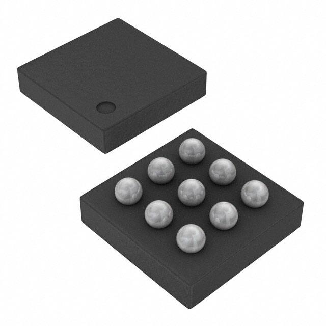


 工商网监
湘ICP备2023018690号
工商网监
湘ICP备2023018690号

