Table of Contents
www.ti.com
User’s Guide
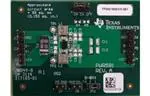
TPS62184 Buck Converter Evaluation Module User's
Guide
ABSTRACT
This user’s guide describes the characteristics, operation, and use of TI's TPS62184 evaluation module
(EVM). The TPS62184EVM-581 (PWR581-002) facilitates the evaluation of the TPS62184 6-A, 2-phase buck
converter. The EVM outputs a 1.8-V output voltage from input voltages between 4 V and 17 V. The TPS62184
features Automatic Efficiency Enhancement ( AEE™) to deliver efficiencies in excess of 90% across the load
current range. The small solution size (99 mm2) and low profile possible enable a very dense power solution in
tablets, Solid State Drives (SSDs), and other portable devices. This user’s guide includes setup instructions for
the hardware, a printed-circuit board layout for the EVM, a schematic diagram, a bill of materials (BOM), and test
results for the EVM.
Table of Contents
1 Introduction.............................................................................................................................................................................2
1.1 Performance Specification................................................................................................................................................. 2
1.2 Modifications...................................................................................................................................................................... 2
2 Setup........................................................................................................................................................................................3
2.1 Input/Output Connector Descriptions................................................................................................................................. 3
2.2 Setup..................................................................................................................................................................................3
3 TPS62184EVM-581 Test Results............................................................................................................................................4
4 Board Layout...........................................................................................................................................................................5
5 Schematic and Bill of Materials.............................................................................................................................................8
5.1 Schematic.......................................................................................................................................................................... 9
5.2 Bill of Materials.................................................................................................................................................................10
6 Revision History................................................................................................................................................................... 10
List of Figures
Figure 3-1. Thermal Performance (VIN = 17 V, Load = 6 A).........................................................................................................4
Figure 3-2. Loop Measurement (VIN = 12 V, Load = 6 A, 50-Ω resistor added in series with R1)............................................... 4
Figure 4-1. Assembly Layer.........................................................................................................................................................5
Figure 4-2. Top Silk Layer............................................................................................................................................................5
Figure 4-3. Top Layer...................................................................................................................................................................6
Figure 4-4. Internal Layer 1......................................................................................................................................................... 6
Figure 4-5. Internal Layer 2......................................................................................................................................................... 7
Figure 4-6. Bottom Layer............................................................................................................................................................. 7
Figure 5-1. TPS62184EVM-581 Schematic.................................................................................................................................9
List of Tables
Table 1-1. Performance Specification Summary..........................................................................................................................2
Table 5-1. TPS62184EVM-581 Bill of Materials.........................................................................................................................10
Trademarks
AEE™ is a trademark of Texas Instruments.
All trademarks are the property of their respective owners.
SLVUAD3A – MARCH 2015 – REVISED MAY 2021
Submit Document Feedback
TPS62184 Buck Converter Evaluation Module User's Guide
Copyright © 2021 Texas Instruments Incorporated
1
�www.ti.com
Introduction
1 Introduction
The TPS62184 is a 6-A, dual-phase, synchronous, step-down converter in a 2 × 3-mm, WCSP package.
1.1 Performance Specification
Table 1-1 provides a summary of the TPS62184EVM-581 performance specifications. All specifications are given
for an ambient temperature of 25°C.
Table 1-1. Performance Specification Summary
Specification
Test Conditions
Input voltage
Min
4
Output voltage setpoint
Output current
Soft-start time
Typ
Max
17
1.8
Unit
V
V
VOUT ≤ 1.8 V
0
6
VOUT > 1.8 V and ≤ 2.5 V
0
5.5
A
VOUT > 2.5 V and ≤ 3.5 V
0
5
A
Ramp time of VOUT
825
A
µs
1.2 Modifications
The output voltage of the EVM may be adjusted within the range stated in the device data sheet. Additional input
and output capacitors can also be added. A lower profile inductor may also be used to reduce the total solution
height. Finally, the input voltage at which the IC turns on can be adjusted with two resistors.
1.2.1 Changing the Output Voltage
The output voltage may be adjusted by changing the values of R1 and R2. Be sure and keep the output voltage
within the range specified in the device data sheet. Setting an output voltage above 1.8 V reduces the maximum
amount of current which can reliably be delivered, per Table 1-1. See the data sheet for details.
1.2.2 Input and Output Capacitors
C13 and C14 are provided for additional input capacitors. These capacitors are not required for proper operation
but can be used to reduce the input voltage ripple.
C7, C8, C9, C10, C11, and C12 are provided for additional output capacitors. These capacitors are not required
for proper operation but can be used to reduce the output voltage ripple and to improve the load transient
response. The total output capacitance must remain within the recommended range in the TPS62184 data sheet
(SLVSCQ5) for proper operation.
1.2.3 Lower Profile Solutions
The TPS62184EVM-581 supports modifications to achieve a lower total solution profile (height). The current
EVM gives a maximum height of 2.1 mm. To obtain a lower profile solution, replace both inductors L1 and L2
with a suitable inductor of lower height. An option is the DFE252012P series from Toko which has a maximum
profile of 1.2 mm. These inductors fit well on the existing pads for L1 and L2.
1.2.4 Configurable Enable Threshold Voltage
With JP1 removed, R4 and R5 can be installed to set a user-selectable input voltage at which the IC turns on.
See the equations in the data sheet for details of calculating the resistor values.
2
TPS62184 Buck Converter Evaluation Module User's Guide
Copyright © 2021 Texas Instruments Incorporated
SLVUAD3A – MARCH 2015 – REVISED MAY 2021
Submit Document Feedback
�www.ti.com
Setup
2 Setup
This section describes how to properly use the TPS62184EVM-581.
2.1 Input/Output Connector Descriptions
J1 – VIN
Positive input connection from the input supply for the EVM
J2 – S+/S–
Input voltage sense connections. Measure the input voltage at this point.
J3 – GND
Return connection from the input supply for the EVM
J4 – VOUT
Output voltage connection
J5 – S+/S–
Output voltage sense connections. Measure the output voltage at this point.
J6 – GND
Output return connection
J7 – PG/GND
The PG output appears on pin 1 of this header with a convenient ground on pin 2
J8 – SS/TR/GND
The SS/TR pin voltage appears on pin 2 of this header with a convenient ground on pin 1
JP1 – EN
EN pin input jumper. Place the supplied jumper across ON and EN to turn on the IC. Place the jumper across
OFF and EN to turn off the IC. Remove the jumper to set a configurable enable threshold voltage with R4 and
R5.
JP2 – PG Pullup Voltage PG pin pullup voltage jumper. Place the supplied jumper on JP2 to connect the PG pin pullup resistor to the
output voltage. Alternatively, the jumper can be removed and a different voltage can be supplied on pin 1 to pull
up the PG pin to a different level. This externally applied voltage must remain below 7 V.
2.2 Setup
To operate the EVM, set jumpers JP1 and JP2 to the desired positions per Section 2.1. Connect the input supply
to J1 and J3 and connect the load to J4 and J6.
SLVUAD3A – MARCH 2015 – REVISED MAY 2021
Submit Document Feedback
TPS62184 Buck Converter Evaluation Module User's Guide
Copyright © 2021 Texas Instruments Incorporated
3
�www.ti.com
TPS62184EVM-581 Test Results
3 TPS62184EVM-581 Test Results
The TPS62184EVM-581 was used to take the data in the TPS62184 data sheet (SLVSCQ5). See the device
data sheet for the performance of this EVM.
Figure 3-1. Thermal Performance (VIN = 17 V, Load = 6 A)
WARNING
Hot surface. Contact may cause burns. Do not touch!
Figure 3-2. Loop Measurement (VIN = 12 V, Load = 6 A, 50-Ω resistor added in series with R1)
4
TPS62184 Buck Converter Evaluation Module User's Guide
Copyright © 2021 Texas Instruments Incorporated
SLVUAD3A – MARCH 2015 – REVISED MAY 2021
Submit Document Feedback
�Board Layout
www.ti.com
4 Board Layout
This section provides the TPS62184EVM-581 board layout and illustrations. The Gerbers are available on
the EVM product page: TPS62184EVM-581. Rev. B of the PCB just filled the vias under U1 to improve
manufacturability. No copper changes were made from Rev. A.
Figure 4-1. Assembly Layer
Figure 4-2. Top Silk Layer
SLVUAD3A – MARCH 2015 – REVISED MAY 2021
Submit Document Feedback
TPS62184 Buck Converter Evaluation Module User's Guide
Copyright © 2021 Texas Instruments Incorporated
5
�www.ti.com
Board Layout
Figure 4-3. Top Layer
Figure 4-4. Internal Layer 1
6
TPS62184 Buck Converter Evaluation Module User's Guide
Copyright © 2021 Texas Instruments Incorporated
SLVUAD3A – MARCH 2015 – REVISED MAY 2021
Submit Document Feedback
�Board Layout
www.ti.com
Figure 4-5. Internal Layer 2
Figure 4-6. Bottom Layer
SLVUAD3A – MARCH 2015 – REVISED MAY 2021
Submit Document Feedback
TPS62184 Buck Converter Evaluation Module User's Guide
Copyright © 2021 Texas Instruments Incorporated
7
�Schematic and Bill of Materials
www.ti.com
5 Schematic and Bill of Materials
This section provides the TPS62184EVM-581 schematic and bill of materials.
8
TPS62184 Buck Converter Evaluation Module User's Guide
SLVUAD3A – MARCH 2015 – REVISED MAY 2021
Submit Document Feedback
Copyright © 2021 Texas Instruments Incorporated
�PC14
www.ti.com
Schematic and Bill of Materials
5.1 Schematic
Figure 5-1 illustrates the TPS62184EVM-581 schematic.
DNP
TP1
XFL4020-102MEB
U1
A1
B1
C1
C1
22µF
D1
E1
F1
C2
22µF
E4
D4
L1
VIN1
VIN1
VIN1
VIN2
VIN2
VIN2
SW1
SW1
SW1
A2
B2
C2
SW2
SW2
SW2
D2
E2
F2
VO
A4
DNP
TP2
L2
EN
R1
187k
SS/TR
FB
B4
PG
F4
AGND
PGND
PGND
PGND
PGND
PGND
PGND
C4
A3
B3
C3
D3
E3
F3
C3
47µF
XFL4020-102MEB
2
C4 DNPC7
47µF
JP2
1
R2
150k
R3
470k
TPS62184YZFR
C5
3300pF
Figure 5-1. TPS62184EVM-581 Schematic
SLVUAD3A – MARCH 2015 – REVISED MAY 2021
Submit Document Feedback
TPS62184 Buck Converter Evaluation Module User's Guide
Copyright © 2021 Texas Instruments Incorporated
9
DNPC8
DN
�Schematic and Bill of Materials
www.ti.com
5.2 Bill of Materials
Table 5-1 lists the BOM for this EVM.
Table 5-1. TPS62184EVM-581 Bill of Materials
Quantity
Ref Des
Value
Description
Size
Part Number
Manufacturer
2
C1, C2
22uF
CAP, CERM, 22uF, 25V, +/-20%, X5R,
0805
0805
GRM21BR61E226ME44L
MuRata
2
C3, C4
47uF
CAP, CERM, 47uF, 10V, +/-20%, X5R,
0805
0805
GRM21BR61A476ME15L
MuRata
1
C5
3300pF
CAP, CERM, 3300pF, 25V, +/-10%, X7R,
0603
0603
GRM188R71E332KA01D
MuRata
1
C6
100uF
CAP, TA, 100uF, 20V, +/-10%, 0.5 ohm,
SMD
7343-43
293D107X9020E2TE3
Vishay-Sprague
2
L1, L2
1uH
Inductor, Shielded, Composite, 1uH, SMD
4x2x4mm
XFL4020-102ME or
XAL4020-102ME
Coilcraft
1
R1
187k
RES, 187k ohm, 1%, 0.1W, 0603
0603
RC0603FR-07187KL
Yageo America
1
R2
150k
RES, 150k ohm, 1%, 0.1W, 0603
0603
RC0603FR-07150KL
Yageo America
1
R3
470k
RES, 470k ohm, 1%, 0.1W, 0603
0603
RC0603FR-07470KL
Yageo America
1
U1
TPS62184
4 - 17V, 6A, 2-Phase Step-Down Converter 2x3mm
TPS62184YZF
Texas Instruments
6 Revision History
NOTE: Page numbers for previous revisions may differ from page numbers in the current version.
Changes from Revision * (March 2015) to Revision A (May 2021)
Page
• Updated user's guide title................................................................................................................................... 2
• Updated the numbering format for tables, figures, and cross-references throughout the document. ................2
10
TPS62184 Buck Converter Evaluation Module User's Guide
Copyright © 2021 Texas Instruments Incorporated
SLVUAD3A – MARCH 2015 – REVISED MAY 2021
Submit Document Feedback
�IMPORTANT NOTICE AND DISCLAIMER
TI PROVIDES TECHNICAL AND RELIABILITY DATA (INCLUDING DATA SHEETS), DESIGN RESOURCES (INCLUDING REFERENCE
DESIGNS), APPLICATION OR OTHER DESIGN ADVICE, WEB TOOLS, SAFETY INFORMATION, AND OTHER RESOURCES “AS IS”
AND WITH ALL FAULTS, AND DISCLAIMS ALL WARRANTIES, EXPRESS AND IMPLIED, INCLUDING WITHOUT LIMITATION ANY
IMPLIED WARRANTIES OF MERCHANTABILITY, FITNESS FOR A PARTICULAR PURPOSE OR NON-INFRINGEMENT OF THIRD
PARTY INTELLECTUAL PROPERTY RIGHTS.
These resources are intended for skilled developers designing with TI products. You are solely responsible for (1) selecting the appropriate
TI products for your application, (2) designing, validating and testing your application, and (3) ensuring your application meets applicable
standards, and any other safety, security, regulatory or other requirements.
These resources are subject to change without notice. TI grants you permission to use these resources only for development of an
application that uses the TI products described in the resource. Other reproduction and display of these resources is prohibited. No license
is granted to any other TI intellectual property right or to any third party intellectual property right. TI disclaims responsibility for, and you
will fully indemnify TI and its representatives against, any claims, damages, costs, losses, and liabilities arising out of your use of these
resources.
TI’s products are provided subject to TI’s Terms of Sale or other applicable terms available either on ti.com or provided in conjunction with
such TI products. TI’s provision of these resources does not expand or otherwise alter TI’s applicable warranties or warranty disclaimers for
TI products.
TI objects to and rejects any additional or different terms you may have proposed. IMPORTANT NOTICE
Mailing Address: Texas Instruments, Post Office Box 655303, Dallas, Texas 75265
Copyright © 2022, Texas Instruments Incorporated
�


 工商网监
湘ICP备2023018690号
工商网监
湘ICP备2023018690号

