Order
Now
Product
Folder
Support &
Community
Tools &
Software
Technical
Documents
TPS62821, TPS62822, TPS62823
SLVSDV6C – NOVEMBER 2017 – REVISED NOVEMBER 2019
TPS6282x 5.5-V, 1-A, 2-A, 3-A Step-Down Converter Family
with 1% Accuracy
1 Features
3 Description
•
•
The TPS6282x is an all-purpose and easy to use
synchronous step-down DC-DC converter with a very
low quiescent current of only 4 µA. It supplies up to
3A output current (TPS62823) from a 2.4-V to 5.5-V
input voltage. Based on the DCS-Control™ topology
it provides a fast transient response.
1
•
•
•
•
•
•
•
•
•
•
•
•
•
•
•
•
DCS-Control™ topology
26-mΩ/25-mΩ internal power switches
(TPS62823)
Up to 3-A output current (TPS62823)
Very low quiescent current of 4 µA
Switching frequency of typically 2.2 MHz
1% feedback voltage accuracy (full temp. range)
Enable (EN) and power good (PG)
Adjustable output voltage from 0.6 V to 4 V
100% duty-cycle mode
Internal soft-start circuitry
Seamless power save mode transition
Undervoltage lockout
Active output discharge
Cycle-by-cycle current limit
HICCUP short-circuit protection
Over temperature protection
CISPR11 class B compliant
Create a custom design using the TPS62822 with
the WEBENCH® Power Designer
The internal reference allows to regulate the output
voltage down to 0.6 V with a high feedback voltage
accuracy of 1% over the junction temperature range
of -40°C to 125°C. The 1-A, 2-A, 3-A scalable pin-topin and BOM-to-BOM compatible device family can
be used with small 470-nH inductors.
The TPS6282x include an automatically entered
power save mode to maintain high efficiency down to
very light loads.
The device features a Power Good signal and an
internal soft start circuit. It is able to operate in 100%
mode. For fault protection, it incorporates a HICCUP
current limit as well as a thermal shutdown.
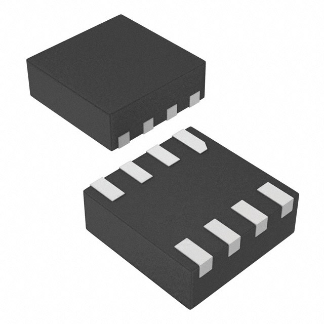
The TPS6282x are packaged in a 2 mm x 1.5 mm
QFN-8 package.
Device Information(1)
PART NUMBER
2 Applications
TPS62821DLC
•
•
•
•
•
•
TPS62822DLC
POL supply in portable/battery powered devices
Factory and building automation
Mobile computing, networking cards
Solid state drive
Data terminal, point of sale
Servers, projectors, printers
Typical Application Schematic
space
space
space
space
470nH
2.4 to 5.5V
VIN
EN
4.7µF
PACKAGE
BODY SIZE (NOM)
QFN (8)
2.00 x 1.50 mm
TPS62823DLC
(1) For all available packages, see the orderable addendum at
the end of the data sheet.
space
space
Efficiency vs Output Current
space
VOUT/2A
SW
TPS62822
R1
Cff*
10µF
VFB=0.6V
PG
FB
±1%
R2
AGND
* optional
PGND
Copyright © 2017, Texas Instruments Incorporated
1
An IMPORTANT NOTICE at the end of this data sheet addresses availability, warranty, changes, use in safety-critical applications,
intellectual property matters and other important disclaimers. PRODUCTION DATA.
�TPS62821, TPS62822, TPS62823
SLVSDV6C – NOVEMBER 2017 – REVISED NOVEMBER 2019
www.ti.com
Table of Contents
1
2
3
4
5
6
7
8
Features ..................................................................
Applications ...........................................................
Description .............................................................
Revision History.....................................................
Device Comparison Table.....................................
Pin Configuration and Functions .........................
Specifications.........................................................
1
1
1
2
3
3
4
7.1
7.2
7.3
7.4
7.5
7.6
4
4
4
4
5
6
Absolute Maximum Ratings ......................................
ESD Ratings ............................................................
Recommended Operating Conditions.......................
Thermal Information ..................................................
Electrical Characteristics...........................................
Typical Characteristics ..............................................
Detailed Description .............................................. 7
8.1 Overview ................................................................... 7
8.2 Functional Block Diagram ......................................... 7
8.3 Feature Description................................................... 8
8.4 Device Functional Modes.......................................... 8
9
Application and Implementation ........................ 10
9.1 Application Information............................................ 10
9.2 Typical Application ................................................. 10
10 Power Supply Recommendations ..................... 21
11 Layout................................................................... 21
11.1 Layout Guidelines ................................................. 21
11.2 Layout Example .................................................... 22
12 Device and Documentation Support ................. 23
12.1
12.2
12.3
12.4
12.5
12.6
12.7
Device Support ....................................................
Related Links ........................................................
Receiving Notification of Documentation Updates
Community Resources..........................................
Trademarks ...........................................................
Electrostatic Discharge Caution ............................
Glossary ................................................................
23
23
23
23
23
23
23
13 Mechanical, Packaging, and Orderable
Information ........................................................... 23
4 Revision History
NOTE: Page numbers for previous revisions may differ from page numbers in the current version.
Changes from Revision B (May 2018) to Revision C
•
Page
Added EMI Performance Curves ......................................................................................................................................... 17
Changes from Revision A (February 2018) to Revision B
•
Page
Changed status for TPS62822 and TPS62823 to Production Data devices........................................................................ 23
Changes from Original (November 2017) to Revision A
•
2
Page
Changed status for TPS62821 to Production Data device................................................................................................... 23
Submit Documentation Feedback
Copyright © 2017–2019, Texas Instruments Incorporated
Product Folder Links: TPS62821 TPS62822 TPS62823
�TPS62821, TPS62822, TPS62823
www.ti.com
SLVSDV6C – NOVEMBER 2017 – REVISED NOVEMBER 2019
5 Device Comparison Table
(1)
Part Number
Output Current
Output Voltage
TPS62821DLC
1A
Adjustable
TPS62822DLC
2A
Adjustable
TPS62823DLC
3A
Adjustable
(1)
For fixed output voltage versions please contact your TI sales representative.
6 Pin Configuration and Functions
space
DLC Package
8 Pin (VQFN)
Top View
EN
1
8
PG
FB
2
7
VIN
AGND
3
6
SW
NC
4
5
PGND
space
Pin Functions
PIN
NAME
NO.
I/O
DESCRIPTION
EN
1
I
Enable input (High=Enabled, Low=Disabled). Do not leave floating.
FB
2
I
Output voltage feedback. Connect resistive voltage divider to this pin.
AGND
3
NC
4
PGND
5
Power
Power ground
SW
6
Power
Switch node, connected to the internal MOSFET switches.
VIN
7
Power
Supply voltage
PG
8
O
Signal ground. Internally connected to the PGND pin. Can be left floating.
Internally not connected. Can be connected to VOUT, GND or left floating.
Power good output. If unused, leave floating or connect to GND.
Copyright © 2017–2019, Texas Instruments Incorporated
Product Folder Links: TPS62821 TPS62822 TPS62823
Submit Documentation Feedback
3
�TPS62821, TPS62822, TPS62823
SLVSDV6C – NOVEMBER 2017 – REVISED NOVEMBER 2019
www.ti.com
7 Specifications
7.1 Absolute Maximum Ratings (1)
MIN
MAX
VIN, FB, EN, PG, NC
-0.3
6
SW (DC)
-0.3
SW (DC, in current limit)
-1.0
SW (AC), less than 10ns (2)
-2.5
10
1
mA
Operating Junction Temperature Range, TJ
-40
150
°C
Storage temperature, Tstg
-65
150
°C
Pin Voltage Range
VIN + 0.3
Power Good Sink Current
(1)
(2)
UNIT
V
Stresses beyond those listed under Absolute Maximum Ratings may cause permanent damage to the device. These are stress ratings
only, which do not imply functional operation of the device at these or any other conditions beyond those indicated under Recommended
Operating Conditions. Exposure to absolute-maximum-rated conditions for extended periods may affect device reliability.
While switching.
7.2 ESD Ratings
VALUE
V(ESD)
(1)
(2)
Electrostatic discharge
Human-body model (HBM), per ANSI/ESDA/JEDEC JS-001 (1)
±2000
Charged-device model (CDM), per JEDEC specification JESD22C101 (2)
±500
UNIT
V
JEDEC document JEP155 states that 500-V HBM allows safe manufacturing with a standard ESD control process.
JEDEC document JEP157 states that 250-V CDM allows safe manufacturing with a standard ESD control process.
7.3 Recommended Operating Conditions
MIN
NOM
MAX
UNIT
Supply Voltage Range, VIN
2.4
5.5
V
Output Voltage Range, VOUT
0.6
4
V
Maximum Output Current, IOUT
TPS62821
1
TPS62822
2
TPS62823
3
Operating Junction Temperature, TJ
-40
125
A
°C
7.4 Thermal Information
TPS6282x
THERMAL METRIC (1)
RθJA
Junction-to-ambient thermal resistance
DLC (VQFN) 8 PINS
UNIT
JEDEC PCB
TPS6282xEVM-005
114.1
69.9
°C/W
(2)
°C/W
RθJC(top)
Junction-to-case (top) thermal resistance
90.2
n/a
RθJB
Junction-to-board thermal resistance
43.4
n/a (2)
°C/W
ψJT
Junction-to-top characterization parameter
6.6
4.3
°C/W
ψJB
Junction-to-board characterization parameter
43.7
44.2
°C/W
RθJC(bot)
Junction-to-case (bottom) thermal resistance
n/a
n/a
°C/W
(1)
(2)
4
For more information about traditional and new thermal metrics, see the Semiconductor and IC Package Thermal Metrics application
report.
Not applicable to an EVM.
Submit Documentation Feedback
Copyright © 2017–2019, Texas Instruments Incorporated
Product Folder Links: TPS62821 TPS62822 TPS62823
�TPS62821, TPS62822, TPS62823
www.ti.com
SLVSDV6C – NOVEMBER 2017 – REVISED NOVEMBER 2019
7.5 Electrical Characteristics
over operating junction temperature range (TJ=-40°C to 125°C) and VIN=2.4V to 5.5V. Typical values at VIN=5V and TJ=25°C
(unless otherwise noted)
PARAMETER
TEST CONDITIONS
MIN
TYP
MAX
UNIT
SUPPLY
VIN
Input Voltage range
2.4
IQ
Operating Quiescent Current
EN=High, IOUT=0A, device not
switching
ISD
Shutdown Current
EN=Low, TJ = -40°C to 85°C
Undervoltage Threshold
Falling Input Voltage
VUVLO
TSD
2.1
Undervoltage Hysteresis
5.5
V
4
10
µA
0.05
0.5
µA
2.2
2.3
V
160
Thermal Shutdown Threshold
Rising Junction Temperature
mV
150
Thermal Shutdown Hysteresis
°C
20
CONTROL (EN, PG)
VH
High-Level Threshold Voltage (EN)
1.0
V
VL
Low-Level Threshold Voltage (EN)
ILKG
Input Leakage Current (EN, PG)
EN = High, VPG = 5V
tSS
Soft-Start Time
Time from EN=High to 95% of VOUT
nominal
VPGTL
Power Good Lower Threshold
Voltage
Rising (VFB vs regulation target)
94%
96%
Falling (VFB vs regulation target)
90%
92%
94%
VPGTH
Power Good Upper Threshold
Voltage
Rising (VFB vs regulation target)
108%
110%
112%
Falling (VFB vs regulation target)
103%
105%
107%
VPGL
Power Good Logic Low Level Output
IPG = -1mA
Voltage
tPGD
Power Good delay
10
0.4
V
100
nA
1.25
ms
98%
0.4
rising
100
falling
20
PWM Mode Operation
2.2
TPS62821
35
TPS62822
35
TPS62823
26
V
µs
POWER SWITCH
FSW
RDS(on)
Switching Frequency
High-Side FET ON-Resistance
Low-Side FET ON-Resistance
ILIM
High-Side FET Current Limit
TPS62821,2,3
MHz
mΩ
25
TPS62821
1.7
2.1
2.4
TPS62822
2.7
3.3
3.7
TPS62823
3.7
4.3
5.0
10
50
nA
594
600
606
mV
75
A
OUTPUT
ILKG_FB
Input Leakage Current (FB)
EN=High, VFB=0.6V
VFB
Feedback Voltage Accuracy
PWM Mode
IDIS
Output Discharge Current
EN=Low, VSW = 0.4V
400
mA
DC Load Regulation
PWM Mode Operation
0.2
%/A
DC Line Regulation
PWM Mode Operation
0.05
%/V
Copyright © 2017–2019, Texas Instruments Incorporated
Product Folder Links: TPS62821 TPS62822 TPS62823
Submit Documentation Feedback
5
�TPS62821, TPS62822, TPS62823
SLVSDV6C – NOVEMBER 2017 – REVISED NOVEMBER 2019
www.ti.com
.0
7.6 Typical Characteristics
6
Figure 1. Quiescent Current
Figure 2. Shutdown Current
Figure 3. High-Side Switch Resistance (TPS62821/2)
Figure 4. High-Side Switch Resistance (TPS62823)
Figure 5. Low-Side Switch Resistance (TPS62821/2/3)
Figure 6. Active Output Discharge Current (EN=Low)
Submit Documentation Feedback
Copyright © 2017–2019, Texas Instruments Incorporated
Product Folder Links: TPS62821 TPS62822 TPS62823
�TPS62821, TPS62822, TPS62823
www.ti.com
SLVSDV6C – NOVEMBER 2017 – REVISED NOVEMBER 2019
8 Detailed Description
8.1 Overview
The TPS6282x are synchronous step-down converters based on the DCS-Control™ topology with an adaptive
constant on-time control and a stabilized switching frequency. It operates in PWM (pulse width modulation) mode
for medium to heavy loads and in PSM (power save mode) at light load conditions, keeping the output voltage
ripple small. The nominal switching frequency is about 2.2MHz with a small and controlled variation over the
input voltage range. As the load current decreases, the converter enters PSM, reducing the switching frequency
to keep efficiency high over the entire load current range. Since combining both PWM and PSM within a single
building block, the transition between modes is seamless and without effect on the output voltage. The devices
offer both excellent dc voltage and fast load transient regulation, combined with a very low output voltage ripple.
8.2 Functional Block Diagram
space
VPGTH
EN
PG
Control Logic
VFB
Soft-Start
UVLO
Thermal
Shutdown
VFB
FB
VPGTL
Ramp
VIN
VSW
VIN
Peak Current Detect
errAmp
VREF
HICCUP
Comp
AGND
Modulator
Gate Drive
VSW
SW
TON
VIN
VSW
Zero Current Detect
NC
VREF
VREF
SW
Discharge
PGND
EN
Copyright © 2017–2019, Texas Instruments Incorporated
Product Folder Links: TPS62821 TPS62822 TPS62823
Submit Documentation Feedback
7
�TPS62821, TPS62822, TPS62823
SLVSDV6C – NOVEMBER 2017 – REVISED NOVEMBER 2019
www.ti.com
8.3 Feature Description
8.3.1 Enable / Shutdown and Output Discharge
The device starts operation, when Enable (EN) is set High. The input threshold levels are typically 0.9V for rising
and 0.7V for falling signals. Do not leave EN floating. Shutdown is forced if EN is pulled Low with a shutdown
current of typically 50nA. During shutdown, the internal power MOSFETs as well as the entire control circuitry are
turned off and the output voltage is actively discharged through the SW pin by a current sink. Therefore, VIN must
remain present for the discharge to function.
8.3.2 Soft-Start
About 250µs after EN goes High, the internal soft-start circuitry controls the output voltage during startup. This
avoids excessive inrush current and ensures a controlled output voltage rise time of about 1ms. It also prevents
unwanted voltage drops from high-impedance power sources or batteries. TPS6282x can start into a pre-biased
output.
8.3.3 Power Good (PG)
The TPS6282x has a built in power good (PG) function. The PG pin goes high impedance, when the output
voltage has reached its nominal value. Otherwise, including when disabled, in UVLO or in thermal shutdown, PG
is Low (see Table 1). The PG function is formed with a window comparator, which has an upper and lower
voltage threshold (see Electrical Characteristics). The PG pin is an open drain output that requires a pull-up
resistor and can sink up to 1mA. If not used, the PG pin can be left floating or connected to GND.
Table 1. Power Good Pin Logic
PG Logic Status
Device State
Enable (EN=High)
High Impedance
VFB ≥ VPGTL and VFB ≤ VPGTH
√
VFB ≤ VPGTL or VFB ≥ VPGTH
√
√
Shutdown (EN=Low)
UVLO
Low
√
0.7 V < VIN < VUVLO
Thermal Shutdown
√
TJ > TSD
Power Supply Removal
VIN < 0.7 V
√
At startup, PG transitions from low to floating about 100µs after the output voltage has reached regulation. Once
in operation, PG has a deglitch delay of about 20µs before going low. When the output voltage returns to
regulation, the same 100µs delay occurs.
8.3.4 Undervoltage Lockout (UVLO)
The undervoltage lockout (UVLO) function prevents misoperation of the device, if the input voltage drops below
the UVLO threshold. It is set to about 2.2V with a hysteresis of typically 160mV.
8.3.5 Thermal Shutdown
The junction temperature (TJ) of the device is monitored by an internal temperature sensor. If TJ exceeds 150°C
(typ.), the device goes in thermal shutdown with a hysteresis of typically 20°C. Once the TJ has decreased
enough, the device resumes normal operation.
8.4 Device Functional Modes
8.4.1 Pulse Width Modulation (PWM) Operation
At load currents larger than half the inductor ripple current, the device operates in pulse width modulation in
continuous conduction mode (CCM).
The PWM operation is based on an adaptive constant on-time control with stabilized switching frequency. To
achieve a stable switching frequency in a steady state condition, the on-time is calculated as:
space
8
Submit Documentation Feedback
Copyright © 2017–2019, Texas Instruments Incorporated
Product Folder Links: TPS62821 TPS62822 TPS62823
�TPS62821, TPS62822, TPS62823
www.ti.com
SLVSDV6C – NOVEMBER 2017 – REVISED NOVEMBER 2019
Device Functional Modes (continued)
TON =
VOUT
× 450ns
VIN
(1)
space
With that, the typical switching frequency is about 2.2MHz.
8.4.2 Power Save Mode (PSM) Operation
To maintain high efficiency at light loads, the device enters power save mode (PSM) at the boundary to
discontinuous conduction mode (DCM). This happens when the output current becomes smaller than half of the
inductor's ripple current. The device operates now with a fixed on-time and the switching frequency further
decreases proportional to the load current. It can be calculated as:
space
fPSM =
2 × IOUT
V éV - VOUT ù
2
× IN ê IN
TON
ú
VOUT ë
L
û
(2)
space
In PSM, the output voltage rises slightly above the nominal target, which can be minimized using larger output
capacitance. At duty cycles larger than 90%, the device may not enter PSM. The device maintains output
regulation in PWM mode.
8.4.3 Minimum Duty Cycle and 100% Mode Operation
There is no limitation for small duty cycles, since even at very low duty cycles the switching frequency is reduced
as needed to always ensure a proper regulation.
If the output voltage level comes close to the input voltage, the device enters 100% mode. While the high-side
switch is constantly turned on, the low-side switch is switched off. The difference between VIN and VOUT is
determined by the voltage drop across the high-side FET and the dc resistance of the inductor. The minimum VIN
that is needed to maintain a specific VOUT value is estimated as:
space
VIN (min) = VOUT + IOUT
( RDS(on ) + RDC(L) )
(3)
space
8.4.4 Current Limit and Short Circuit Protection
The peak switch current of TPS6282x is internally limited, cycle by cycle, to a maximum dc value as specified in
Electrical Characteristics. This prevents the device from drawing excessive current in case of externally caused
over current or short circuit condition. Due to an internal propagation delay of about 60ns, the actual ac peak
current can exceed the static current limit during that time.
If the current limit threshold is reached, the device delivers its maximum output current. Detecting this condition
for 32 switching cycles (about 13µs), the device turns off the high-side MOSFET for about 100µs which allows
the inductor current to decrease through the low-side MOSFET's body diode and then restarts again with a soft
start cycle. As long as the overload condition is present, the device hiccups that way, limiting the output power.
Copyright © 2017–2019, Texas Instruments Incorporated
Product Folder Links: TPS62821 TPS62822 TPS62823
Submit Documentation Feedback
9
�TPS62821, TPS62822, TPS62823
SLVSDV6C – NOVEMBER 2017 – REVISED NOVEMBER 2019
www.ti.com
9 Application and Implementation
space
NOTE
Information in the following applications sections is not part of the TI component
specification, and TI does not warrant its accuracy or completeness. TI’s customers are
responsible for determining suitability of components for their purposes. Customers should
validate and test their design implementation to confirm system functionality.
space
9.1 Application Information
The TPS6282x is a switched mode step-down converter, able to convert a 2.4-V to 5.5-V input voltage into a
lower 0.6-V to 4-V output voltage, providing up to 3A continuous output current (TPS62823). It needs a very low
amount of external components. Apart from the inductor and the output and input capacitors, additional parts are
only needed to set the output voltage and to enable the Power Good (PG) feature.
9.2 Typical Application
space
470nH
2.4 to 5.5V
VOUT/2A
SW
VIN
VPG
C1
EN
R3
TPS62822
R1
Cff*
C2
C3*
FB
PG
R2
AGND
PGND
Copyright © 2017, Texas Instruments Incorporated
* optional
Figure 7. A typical 2.4 to 5.5-V, 2-A Power Supply
space
9.2.1 Design Requirements
The following design guideline provides a range for the component selection to operate within the recommended
operating conditions. Table 2 shows the components selection that was used for the measurements shown in the
Application Curves.
Table 2. List of Components
REFERENCE
DESCRIPTION
MANUFACTURER
IC
5.5-V, step-down converter
L1
470 nH ±20%, 7.6mΩ DCR, 6.6A ISAT
C1
4.7 µF ±20%, 6.3V, ceramic, 0603, X7R
JMK107BB7475MA-T, Taiyo Yuden
C2, C3
10 µF ±20%, 10V, ceramic, 0603, X7R
GRM188Z71A106MA73D, MuRata
Cff
120pF ±5%, 50V, 0603
GRM1885C1H121JA01D, MuRata
R1, R2
Depending on VOUT, chip, 0603
Standard
R3
100-kΩ, chip, 0603, 0.1W, 1%
Standard
10
Submit Documentation Feedback
TPS6282xDLC, Texas Instruments
XFL4015-471MEB, Coilcraft
Copyright © 2017–2019, Texas Instruments Incorporated
Product Folder Links: TPS62821 TPS62822 TPS62823
�TPS62821, TPS62822, TPS62823
www.ti.com
SLVSDV6C – NOVEMBER 2017 – REVISED NOVEMBER 2019
9.2.2 Detailed Design Procedure
9.2.2.1 Custom Design With WEBENCH® Tools
Click here to create a custom design using the TPS62822 device with the WEBENCH® Power Designer.
1. Start by entering the input voltage (VIN), output voltage (VOUT), and output current (IOUT) requirements.
2. Optimize the design for key parameters such as efficiency, footprint, and cost using the optimizer dial.
3. Compare the generated design with other possible solutions from Texas Instruments.
The WEBENCH Power Designer provides a customized schematic along with a list of materials with real-time
pricing and component availability.
In most cases, these actions are available:
• Run electrical simulations to see important waveforms and circuit performance
• Run thermal simulations to understand board thermal performance
• Export customized schematic and layout into popular CAD formats
• Print PDF reports for the design, and share the design with colleagues
Get more information about WEBENCH tools at www.ti.com/WEBENCH.
9.2.2.2 Setting the Adjustable Output Voltage
Choose resistors R1 and R2 to set the output voltage within a range of 0.6V to 4V, according to Equation 4. To
keep the feedback (FB) net robust from noise, set R2 equal to or lower than 120kΩ to have at least 5µA of
current in the voltage divider. Lower values of FB resistors achieve better noise immunity, and lower light load
efficiency, as explained in SLYT469.
space
§V
R1 R2 u ¨ OUT
© VFB
·
1¸
¹
§V
R2 u ¨ OUT
© 0.6V
·
1¸
¹
(4)
space
9.2.2.3 Feed-forward Capacitor Selection
A feedforward capacitor (CFF) is recommended in parallel with R1. Equation 5 calculates the CFF value. For the
recommended 100k value for R2, a 120 pF feed forward capacitor is used.
space
Cff =
12ms
R2
(5)
space
Figure 47 and Figure 48 show the results of a frequency domain analysis for both use cases, with and without a
feed-forward capacitor. The larger unity gain frequency, caused by the feed forward capacitor, results in a
significant improvement of the transient response.
space
9.2.2.4 Output Filter Selection
The TPS6282x is internally compensated and optimized for a range of output filter component values, which is
specified in Table 3. Using these values simplifies the output filter component selection. Checked cells represent
combinations that are proven for stability by simulation and lab test. Further combinations are possible, but
should be checked for each individual application.
Copyright © 2017–2019, Texas Instruments Incorporated
Product Folder Links: TPS62821 TPS62822 TPS62823
Submit Documentation Feedback
11
�TPS62821, TPS62822, TPS62823
SLVSDV6C – NOVEMBER 2017 – REVISED NOVEMBER 2019
www.ti.com
Table 3. Recommended LC Output Filter Combinations (1)
4.7 µF
10 µF
2 x 10µF or 22 µF
47 µF
100 µF
√
√ (3)
150 µF
0.33 µH
√
0.47 µH
√
1.0 µH
(2)
√
√
√
(3)
√ (3)
1.5 µH
(1)
(2)
(3)
The values in the table are the nominal values of inductors and ceramic capacitors. The effective capacitance can vary depending on
package size, voltage rating and dielectric material (typical variations are from +20% to -50%).
This combination is recommended as the standard value for most of all applications.
Cff is recommended for large COUT values.
9.2.2.5 Inductor Selection
The TPS6282x is designed to work with inductors of 470nH nominal and can be used with 1µH inductors as well.
The inductor has to be selected for adequate saturation current and a low dc resistance (DCR). The minimum
inductor current rating, that is needed under static load conditions is calculated using Equation 6 and Equation 7.
space
I peak (max) = I L(min) = IOUT (max) +
DI L(max)
2
(6)
space
DIL(max)
V
æ
ç 1 - OUT
ç
VIN
= VOUT ç
ç L(min) × fSW
ç
è
ö
÷
÷
÷
÷
÷
ø
(7)
space
This calculation gives the minimum saturation current of the inductor needed and an additional margin is
recommended to cover dynamic overshoot due to startup or load transients. Inductors are available in different
dimensions. Choosing the smallest size might result in less efficiency due to larger DCR and ac losses. The
following inductors have been tested with the TPS6282x:
Table 4. List of Recommended Inductors
TYPE
Nominal
INDUCTANCE
(1)
Saturation Current and DC
Resistance
max. ISAT [A]
(3)
Dimensions [mm]
Manufacturer (2)
max. RDC [mΩ]
HTEN20161T-R47MDR
0.47
4.8
32
2.0 x 1.6 x 1.0
Cyntec
HTEH20121T-R47MSR
0.47
4.6
25
2.0 x 1.2 x 1.0
Cyntec
DFE201610E - R47M
0.47
4.8
32
2.0 x 1.6 x 1.0
muRata
DFE201210S - R47M
0.47
4.8
32
2.0 x 1.2 x 1.0
muRata
TFM201610ALM-R47MTAA
0.47
5.1
34
2.0 x 1.6 x 1.0
TDK
TFM201610ALC-R47MTAA
0.47
5.2
25
2.0 x 1.6 x 1.0
TDK
XFL4015-471ME
0.47
6.6
8.36
4.0 x 4.0 x 1.6
Coilcraft
(1)
(2)
(3)
Inductance Tolerance ±20%
See Third-party Products disclaimer.
ΔL/L≈30%
12
Submit Documentation Feedback
Copyright © 2017–2019, Texas Instruments Incorporated
Product Folder Links: TPS62821 TPS62822 TPS62823
�TPS62821, TPS62822, TPS62823
www.ti.com
SLVSDV6C – NOVEMBER 2017 – REVISED NOVEMBER 2019
9.2.2.6 Output Capacitor Selection
The output voltage range of TPS6282x is 0.6V to 4V. While stability is a first criteria for the output filter selection
(L and COUT), the output capacitor value also determines transient response behavior and ripple of VOUT. The
recommended typical value for the output capacitor is 2x10µF (or 1x 22µF) and can be small ceramic capacitors
with low equivalent series resistance (ESR). For lower VOUT (VOUT ≤ 2V) and where only moderate load
transients are present, 10µF can be sufficient. In either case a minimum effective output capacitance of 5µF
should be present.
To keep low resistance and to get a narrow capacitance variation with temperature, it is recommended to use
X7R or X5R dielectric. Using an even higher value has advantages like smaller voltage ripple and tighter output
voltage accuracy in PSM.
9.2.2.7 Input Capacitor Selection
For typical application, an input capacitor of 4.7µF is sufficient and recommended. A larger value reduces input
current ripple further. The input capacitor buffers the input voltage for transient events and also decouples the
converter from the supply. A low ESR ceramic capacitor is recommended for best filtering and should be placed
between VIN and PGND as close as possible to those pins. In either case a minimum effective input capacitance
of 3µF should be present.
Copyright © 2017–2019, Texas Instruments Incorporated
Product Folder Links: TPS62821 TPS62822 TPS62823
Submit Documentation Feedback
13
�TPS62821, TPS62822, TPS62823
SLVSDV6C – NOVEMBER 2017 – REVISED NOVEMBER 2019
www.ti.com
9.2.3 Application Curves
VIN=5V, VOUT=1.8V, TA=25°C, BOM = Table 2, (unless otherwise noted)
100% mode
100% mode
Figure 8. Efficiency TPS62821 at VOUT=3.3V
Figure 9. Efficiency TPS62821 at VOUT=3.3V
100% mode
100% mode
Figure 10. Efficiency TPS62822 at VOUT=3.3V
Figure 11. Efficiency TPS62822 at VOUT=3.3V
100% mode
100% mode
Figure 12. Efficiency TPS62823 at VOUT=3.3V
14
Submit Documentation Feedback
Figure 13. Efficiency TPS62823 at VOUT=3.3V
Copyright © 2017–2019, Texas Instruments Incorporated
Product Folder Links: TPS62821 TPS62822 TPS62823
�TPS62821, TPS62822, TPS62823
www.ti.com
SLVSDV6C – NOVEMBER 2017 – REVISED NOVEMBER 2019
Figure 14. Efficiency TPS62821 at VOUT=1.8V
Figure 15. Efficiency TPS62821 at VOUT=1.8V
Figure 16. Efficiency TPS62822 at VOUT=1.8V
Figure 17. Efficiency TPS62822 at VOUT=1.8V
Figure 18. Efficiency TPS62823 at VOUT=1.8V
Figure 19. Efficiency TPS62823 at VOUT=1.8V
Copyright © 2017–2019, Texas Instruments Incorporated
Product Folder Links: TPS62821 TPS62822 TPS62823
Submit Documentation Feedback
15
�TPS62821, TPS62822, TPS62823
SLVSDV6C – NOVEMBER 2017 – REVISED NOVEMBER 2019
16
www.ti.com
Figure 20. Efficiency TPS62821 at VOUT=1V
Figure 21. Efficiency TPS62821 at VOUT=1V
Figure 22. Efficiency TPS62822 at VOUT=1V
Figure 23. Efficiency TPS62822 at VOUT=1V
Figure 24. Efficiency TPS62823 at VOUT=1V
Figure 25. Efficiency TPS62823 at VOUT=1V
Submit Documentation Feedback
Copyright © 2017–2019, Texas Instruments Incorporated
Product Folder Links: TPS62821 TPS62822 TPS62823
�TPS62821, TPS62822, TPS62823
www.ti.com
SLVSDV6C – NOVEMBER 2017 – REVISED NOVEMBER 2019
Figure 26. Efficiency TPS62821 at VOUT=0.6V
Figure 27. Efficiency TPS62821 at VOUT=0.6V
Figure 28. Efficiency TPS62822 at VOUT=0.6V
Figure 29. Efficiency TPS62822 at VOUT=0.6V
Figure 30. Efficiency TPS62823 at VOUT=0.6V
Figure 31. Efficiency TPS62823 at VOUT=0.6V
Copyright © 2017–2019, Texas Instruments Incorporated
Product Folder Links: TPS62821 TPS62822 TPS62823
Submit Documentation Feedback
17
�TPS62821, TPS62822, TPS62823
www.ti.com
Figure 32. Output Voltage Accuracy (Load Regulation)
Figure 33. Output Voltage Accuracy (Line Regulation)
Figure 34. Switching Frequency vs Output Current
Figure 35. Switching Frequency vs Input Voltage
70
65
60
55
50
45
40
35
30
25
20
15
10
5
30
Horizontal - QPK
Vertical - QPK
CISPR11 Group 1 Class B 3m QP
Level (dBPV/m)
Level (dBPV/m)
SLVSDV6C – NOVEMBER 2017 – REVISED NOVEMBER 2019
40 50 6070
100
200
300 400500
Frequency (MHz)
700 1000
RLOAD = 2.20 Ω, VIN = 5.5 V (battery supply), VOUT = 1.8 V, EMI
test board without filters
Figure 36. TPS62821 Radiated Emission
18
Submit Documentation Feedback
70
65
60
55
50
45
40
35
30
25
20
15
10
5
30
Horizontal - QPK
Vertical - QPK
CISPR11 Group 1 Class B 3m QP
40 50 6070
100
200
300 400500
Frequency (MHz)
700 1000
RLOAD = 1.00 Ω, VIN = 5.5 V (battery supply), VOUT = 1.8 V, EMI
test board without filters
Figure 37. TPS62822 Radiated Emission
Copyright © 2017–2019, Texas Instruments Incorporated
Product Folder Links: TPS62821 TPS62822 TPS62823
�TPS62821, TPS62822, TPS62823
Level (dBPV/m)
www.ti.com
70
65
60
55
50
45
40
35
30
25
20
15
10
5
30
SLVSDV6C – NOVEMBER 2017 – REVISED NOVEMBER 2019
Horizontal - QPK
Vertical - QPK
CISPR11 Group 1 Class B 3m QP
40 50 6070
100
200
300 400500
Frequency (MHz)
700 1000
RLOAD = 0.68 Ω, VIN = 5.5 V (battery supply), VOUT = 1.8 V, EMI
test board without filters
COUT=2x10µF
IOUT=1A
Figure 39. Typical Operation PWM
Figure 38. TPS62823 Radiated Emission
COUT=2x10µF
IOUT=0.1A
Figure 40. Typical Operation PSM
COUT=2x10µF
COUT=2x10µF
Figure 41. Startup into 0.6-Ohm (TPS62823)
COUT=2x10µF
Figure 42. Startup at No Load
Figure 43. Active Output Discharge at load 1.8-Ohm
Copyright © 2017–2019, Texas Instruments Incorporated
Product Folder Links: TPS62821 TPS62822 TPS62823
Submit Documentation Feedback
19
�TPS62821, TPS62822, TPS62823
SLVSDV6C – NOVEMBER 2017 – REVISED NOVEMBER 2019
COUT=2x10µF
COUT=2x10µF
Figure 44. Active Output Discharge at No Load
COUT=2x10µF
www.ti.com
Cff=120pF
Figure 45. Load Transient Response, 50mA to 1A,
TPS62822
Cff=120pF
Figure 46. Load Transient Response, 1A to 2A, TPS62822
COUT=2x10µF
no CFF
Figure 47. Frequency Response (TPS62823), IOUT=3A
20
Submit Documentation Feedback
Copyright © 2017–2019, Texas Instruments Incorporated
Product Folder Links: TPS62821 TPS62822 TPS62823
�TPS62821, TPS62822, TPS62823
www.ti.com
SLVSDV6C – NOVEMBER 2017 – REVISED NOVEMBER 2019
Figure 49. Overload Response of TPS62823
COUT=2x10µF
CFF=120pF
Figure 48. Frequency Response (TPS62823), IOUT=3A
Figure 50. Overload Response of TPS62823 (Hiccup cycle)
Figure 51. Device Temperature Rise on TPS62823 EVM at
IOUT=3A
10 Power Supply Recommendations
The TPS6282x is designed to operate from a 2.4-V to 5.5-V input voltage supply. The input power supply's
output current needs to be rated according to the output voltage and the output current of the power rail
application.
11 Layout
11.1 Layout Guidelines
The recommended PCB layout for the TPS6282x is shown below. It ensures best electrical and optimized
thermal performance considering the following important topics:
- The input capacitor(s) must be placed as close as possible to the VIN and PGND pins of the device. This
provides low resistive and inductive paths for the high di/dt input current.
- The SW node connection from the IC to the inductor conducts alternating high currents. It should be kept short.
Copyright © 2017–2019, Texas Instruments Incorporated
Product Folder Links: TPS62821 TPS62822 TPS62823
Submit Documentation Feedback
21
�TPS62821, TPS62822, TPS62823
SLVSDV6C – NOVEMBER 2017 – REVISED NOVEMBER 2019
www.ti.com
Layout Guidelines (continued)
- The VOUT regulation loop is closed with COUT and its ground connection. To avoid load regulation and EMI
noise, the loop should be kept short.
- The FB node is sensitive to dv/dt signals. Therefore the resistive divider should be placed close to the FB and
AGND pins.
For more detailed information about the actual EVM solution, see the EVM users guide.
11.2 Layout Example
space
space
space
VOUT
L1
VIN
C1
SW
PGND
GND
NC
AGND
VIN
PG
EN
FB
GND
C2 C3
R2
R1
Cff
Figure 52. TPS6282x Board Layout
22
Submit Documentation Feedback
Copyright © 2017–2019, Texas Instruments Incorporated
Product Folder Links: TPS62821 TPS62822 TPS62823
�TPS62821, TPS62822, TPS62823
www.ti.com
SLVSDV6C – NOVEMBER 2017 – REVISED NOVEMBER 2019
12 Device and Documentation Support
12.1 Device Support
12.1.1 Third-Party Products Disclaimer
TI'S PUBLICATION OF INFORMATION REGARDING THIRD-PARTY PRODUCTS OR SERVICES DOES NOT
CONSTITUTE AN ENDORSEMENT REGARDING THE SUITABILITY OF SUCH PRODUCTS OR SERVICES
OR A WARRANTY, REPRESENTATION OR ENDORSEMENT OF SUCH PRODUCTS OR SERVICES, EITHER
ALONE OR IN COMBINATION WITH ANY TI PRODUCT OR SERVICE.
12.2 Related Links
The table below lists quick access links. Categories include technical documents, support and community
resources, tools and software, and quick access to order now.
Table 5. Related Links
PARTS
PRODUCT FOLDER
ORDER NOW
TECHNICAL
DOCUMENTS
TOOLS &
SOFTWARE
SUPPORT &
COMMUNITY
TPS62821
Click here
Click here
Click here
Click here
Click here
TPS62822
Click here
Click here
Click here
Click here
Click here
TPS62823
Click here
Click here
Click here
Click here
Click here
12.3 Receiving Notification of Documentation Updates
To receive notification of documentation updates, navigate to the device product folder on ti.com. In the upper
right corner, click on Alert me to register and receive a weekly digest of any product information that has
changed. For change details, review the revision history included in any revised document.
12.4 Community Resources
TI E2E™ support forums are an engineer's go-to source for fast, verified answers and design help — straight
from the experts. Search existing answers or ask your own question to get the quick design help you need.
Linked content is provided "AS IS" by the respective contributors. They do not constitute TI specifications and do
not necessarily reflect TI's views; see TI's Terms of Use.
12.5 Trademarks
DCS-Control, E2E are trademarks of Texas Instruments.
All other trademarks are the property of their respective owners.
12.6 Electrostatic Discharge Caution
This integrated circuit can be damaged by ESD. Texas Instruments recommends that all integrated circuits be handled with
appropriate precautions. Failure to observe proper handling and installation procedures can cause damage.
ESD damage can range from subtle performance degradation to complete device failure. Precision integrated circuits may be more
susceptible to damage because very small parametric changes could cause the device not to meet its published specifications.
12.7 Glossary
SLYZ022 — TI Glossary.
This glossary lists and explains terms, acronyms, and definitions.
13 Mechanical, Packaging, and Orderable Information
The following pages include mechanical, packaging, and orderable information. This information is the most
current data available for the designated devices. This data is subject to change without notice and revision of
this document. For browser-based versions of this data sheet, refer to the left-hand navigation.
Copyright © 2017–2019, Texas Instruments Incorporated
Product Folder Links: TPS62821 TPS62822 TPS62823
Submit Documentation Feedback
23
�PACKAGE OPTION ADDENDUM
www.ti.com
10-Dec-2020
PACKAGING INFORMATION
Orderable Device
Status
(1)
Package Type Package Pins Package
Drawing
Qty
Eco Plan
(2)
Lead finish/
Ball material
MSL Peak Temp
Op Temp (°C)
Device Marking
(3)
(4/5)
(6)
TPS62821DLCR
ACTIVE
VSON-HR
DLC
8
3000
RoHS & Green
Call TI | NIPDAU
Level-1-260C-UNLIM
-40 to 125
A1
TPS62821DLCT
ACTIVE
VSON-HR
DLC
8
250
RoHS & Green
Call TI | NIPDAU
Level-1-260C-UNLIM
-40 to 125
A1
TPS62822DLCR
ACTIVE
VSON-HR
DLC
8
3000
RoHS & Green
Call TI | NIPDAU
Level-1-260C-UNLIM
-40 to 125
A2
TPS62822DLCT
ACTIVE
VSON-HR
DLC
8
250
RoHS & Green
Call TI | NIPDAU
Level-1-260C-UNLIM
-40 to 125
A2
TPS62823DLCR
ACTIVE
VSON-HR
DLC
8
3000
RoHS & Green
NIPDAU
Level-1-260C-UNLIM
-40 to 125
A3
TPS62823DLCT
ACTIVE
VSON-HR
DLC
8
250
RoHS & Green
NIPDAU
Level-1-260C-UNLIM
-40 to 125
A3
(1)
The marketing status values are defined as follows:
ACTIVE: Product device recommended for new designs.
LIFEBUY: TI has announced that the device will be discontinued, and a lifetime-buy period is in effect.
NRND: Not recommended for new designs. Device is in production to support existing customers, but TI does not recommend using this part in a new design.
PREVIEW: Device has been announced but is not in production. Samples may or may not be available.
OBSOLETE: TI has discontinued the production of the device.
(2)
RoHS: TI defines "RoHS" to mean semiconductor products that are compliant with the current EU RoHS requirements for all 10 RoHS substances, including the requirement that RoHS substance
do not exceed 0.1% by weight in homogeneous materials. Where designed to be soldered at high temperatures, "RoHS" products are suitable for use in specified lead-free processes. TI may
reference these types of products as "Pb-Free".
RoHS Exempt: TI defines "RoHS Exempt" to mean products that contain lead but are compliant with EU RoHS pursuant to a specific EU RoHS exemption.
Green: TI defines "Green" to mean the content of Chlorine (Cl) and Bromine (Br) based flame retardants meet JS709B low halogen requirements of