Product
Folder
Sample &
Buy
Support &
Community
Tools &
Software
Technical
Documents
TPS65030
SLVS620C – JULY 2007 – REVISED SEPTEMBER 2015
TPS65030 Power-Management IC for USB-OTG
1 Features
3 Description
•
The TPS65030 device contains three charge pumps
and one LDO to generate all supply voltages
necessary
for
a
USB
On-The-Go
(OTG)
implementation using TUSB6010. The charge pumps
are optimized for a single Li-Ion cell input or for 5 V
from the USB bus. The input voltage range is 3 V to
5 V for the battery voltage. High efficiency is achieved
by using fractional conversion techniques for the
charge pumps in combination with a power saving
sleep mode. The current-controlled charge pumps
ensure low input current ripple and low EMI. Small
sized external ceramic capacitors are required to
build a complete power-supply solution. To reduce
board space to a minimum, the device switches at
1-MHz operating frequency and is available in a small
25-ball chip scale package (YZK).
1
•
•
•
•
•
•
•
•
•
•
•
Four Regulated Output Voltages With 3%
Tolerance
– Fractional Charge Pump for 5 V, 100 mA
– Fractional Charge Pump for 1.5 V, 200 mA
– Doubling Charge Pump With LDO Mode for
3.3 V, 22 mA
– LDO for 1.8 V, 60 mA
Switching Frequency 1 MHz
3-V to 5-V Operating Input Voltage Range at VCC
Pin
Sleep Mode Sets Vout2 and Vout3 Into LDO
Mode
Sleep Mode Reduces Quiescent Current of Vout2,
Vout3, and Vout4 to 8-μA Each
Internal Bus Switch
Vbus Comparator
Internal Soft Start Limits Inrush Current
Low Input Current Ripple and Low EMI
Overcurrent and Overtemperature Protected
Undervoltage Lockout With Hysteresis
Ultra-Small 2.50-mm × 2.70-mm Chip Scale
Package Applications
2 Applications
•
Power Supply for USB OTG for:
– Cellular Phones
– Smart Phones
– PDAs
– Handheld PCs
– Digital Cameras
– Camcorders
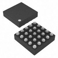
Device Information(1)
PART NUMBER
TPS65030
PACKAGE
DSBGA (25)
BODY SIZE (MAX)
2.51 mm × 2.70 mm
(1) For all available packages, see the orderable addendum at
the end of the data sheet.
spacing
spacing
Functional Block Diagram
TPS65030
3 V . . .4.2 V (5 V)
10 mF
VIN
Vbus
5 V/100 mA
4.7 mF
VIN
EN1 (5 V)
C o1
Charge CF1A+
Pump
CF1A−
EN2 (3.3 V
and 1.5 V)
CF1B+
1 mF
1 mF
CF1B−
EN3 (1.8 V)
Vout2
SLEEP
3.3 V/22 mA
C o2
1 mF
PGood
SW_EN1
Charge
Pump
CF2+
100 nF
CF2−
SW_EN2
Vout3
Test SRP
C o3
1.5 V/200 mA
10 mF
Charge
Pump
PGND
CF3+
CF3−
1 mF
PGND
GND
Vout4
LDO
1.8 V/60 mA
C o4
1 mF
1
An IMPORTANT NOTICE at the end of this data sheet addresses availability, warranty, changes, use in safety-critical applications,
intellectual property matters and other important disclaimers. PRODUCTION DATA.
�TPS65030
SLVS620C – JULY 2007 – REVISED SEPTEMBER 2015
www.ti.com
Table of Contents
1
2
3
4
5
6
7
Features ..................................................................
Applications ...........................................................
Description .............................................................
Revision History.....................................................
Pin Configuration and Functions .........................
Specifications.........................................................
1
1
1
2
3
4
6.1
6.2
6.3
6.4
6.5
6.6
6.7
4
4
4
5
5
8
9
Absolute Maximum Ratings ......................................
ESD Ratings ............................................................
Recommended Operating Conditions.......................
Thermal Information .................................................
Electrical Characteristics...........................................
Timing Requirements ................................................
Typical Characteristics ..............................................
Detailed Description ............................................ 10
7.1 Overview ................................................................. 10
7.2 Functional Block Diagrams ..................................... 10
7.3 Feature Description................................................. 11
7.4 Device Functional Modes........................................ 14
8
Application and Implementation ........................ 16
8.1 Application Information............................................ 16
8.2 Typical Application ................................................. 16
9
Power Supply Recommendations...................... 20
9.1 Power Dissipation ................................................... 20
10 Layout................................................................... 22
10.1 Layout Guidelines ................................................. 22
10.2 Layout Example .................................................... 22
11 Device and Documentation Support ................. 23
11.1
11.2
11.3
11.4
11.5
Device Support ....................................................
Community Resources..........................................
Trademarks ...........................................................
Electrostatic Discharge Caution ............................
Glossary ................................................................
23
23
23
23
23
12 Mechanical, Packaging, and Orderable
Information ........................................................... 23
4 Revision History
NOTE: Page numbers for previous revisions may differ from page numbers in the current version.
Changes from Revision B (July 2007) to Revision C
•
2
Page
Added ESD Ratings table, Feature Description section, Device Functional Modes, Application and Implementation
section, Power Supply Recommendations section, Layout section, Device and Documentation Support section, and
Mechanical, Packaging, and Orderable Information section .................................................................................................. 1
Submit Documentation Feedback
Copyright © 2007–2015, Texas Instruments Incorporated
Product Folder Links: TPS65030
�TPS65030
www.ti.com
SLVS620C – JULY 2007 – REVISED SEPTEMBER 2015
5 Pin Configuration and Functions
YZK Package
25-Pin DSBGA
Bottom View
E5
D5
C5
B5
A5
E4
D4
C4
B4
A4
E3
D3
C3
B3
A3
E2
D2
C2
B2
A2
E1
D1
C1
B1
A1
Pin Functions
PIN
I/O
LOGIC FUNCTION
C1
—
—
Connect to the flying capacitor CF1A
E1
—
—
Connect to the flying capacitor CF1A
CF1B+
B1
—
—
Connect to the flying capacitor CF1B
CF1B–
D1
—
—
Connect to the flying capacitor CF1B
CF2+
D5
—
—
Connect to the flying capacitor CF2
CF2–
E5
—
—
Connect to the flying capacitor CF2
CF3+
A3
—
—
Connect to the flying capacitor CF3
CF3–
A5
—
—
Connect to the flying capacitor CF3
NAME
NO.
CF1A+
CF1A–
DESCRIPTION
EN1
B3
I
1 = Vbus converter enabled
0 = Vbus converter disabled
EN2
B4
I
1 = Vout2 and Vout3 enabled
0 = Vout2 and Vout3 disabled
Enable input for 3.3-V and 1.5-V charge pump. Logic low forces both charge pumps into
shutdown mode reducing the supply current to less than 1 μA.
EN3
C4
I
1 = Vout4 enabled
0 = Vout4 disabled
Enable input for 1.8-V LDO. Logic low forces the LDO into shutdown mode reducing the
supply current to less than 1 μA. To ensure that EN3 is pulled to GND when left open, there
is an internal pulldown resistor to GND.
GND
D4
—
E2, B5
—
PGND
Enable input for 5-V charge pump. A logic low forces the charge pump into shutdown mode
reducing the supply current to less than 1 μA.
—
Analog ground
—
Power ground
PGood
D3
O
1 = output voltage within limits
0 = output voltage too low
SLEEP
B2
I
1 = sleep mode
0 = normal mode
This pin is used to set the 3.3-V and 1.5-V charge pump as well as the 1.8-V LDO into
sleep mode. Logic low forces the charge pumps into normal operating mode if they are
enabled.
SW_EN1
C3
I
1 = Vout3 switchover to Vbus
enabled
0 = Vout3 is battery powered
Enable input 1 for internal USB switch. If this input is pulled high, the Vout3 converter is
powered from Vbus. If SLEEP is pulled high, the converter is always powered from the
battery, independent from the state of SW_EN1.
SW_EN2
C2
I
1 = Vout2 switchover to Vbus
enabled
0 = Vout2 is battery powered
Enable input 2 for internal USB switch. If this input is pulled high, the Vout2 converter is
powered from Vbus. If SLEEP is pulled high, the converter is always powered from the
battery, independent from the state of SW_EN2.
Test
SRP
D2
I/O
Input:
1 = IO at Vbus = 100 mA
0 = IO at Vbus = 1 mA
Open-drain output for connectivity test, input for current limit during start-up for Vbus
voltage if the device is not in test mode. If Test SRP is pulled high, the Vbus current during
startup is > 100 mA. If pulled low, it is 1 mA.
Vbus
E3
I/O
—
Output for the 5-V charge pump. Connect the output capacitor directly to this pin. This pin is
also the input for the 5-V from the USB port, if the USB port powers the 3.3-V and 1.5-V
charge pump as well as the 1.8-V LDO.
VIN
Open drain power good output for Vout2,Vout3, and Vout4
A1, A2
I
—
Supply voltage input
Vout2
C5
O
—
Output for the 3.3-V charge pump. Connect Cout2 directly to this pin.
Vout3
A4
O
—
Output for the 1.5-V charge pump. Connect Cout3 directly to this pin.
Vout4
E4
O
—
Output for the 1.8-V LDO. Connect Cout4 directly to this pin.
Submit Documentation Feedback
Copyright © 2007–2015, Texas Instruments Incorporated
Product Folder Links: TPS65030
3
�TPS65030
SLVS620C – JULY 2007 – REVISED SEPTEMBER 2015
www.ti.com
6 Specifications
6.1 Absolute Maximum Ratings
over operating free-air temperature range (unless otherwise noted)
(1)
MIN
MAX
UNIT
Supply voltage, VS
VIN, Vbus
–0.3
7
V
Voltage
EN1, EN2, EN3, SLEEP, SW_EN1, SW_EN2, PG, Test SRP
–0.3
Output current, IO
VIN
V
Vbus
200
mA
Vout2
40
mA
Vout3
300
mA
Vout4
100
mA
150
°C
Maximum junction temperature, TJ
Operating free-air temperature, TA
–40
85
°C
Storage temperature, Tstg
–65
150
°C
(1)
Stresses beyond those listed under Absolute Maximum Ratings may cause permanent damage to the device. These are stress ratings
only, which do not imply functional operation of the device at these or any other conditions beyond those indicated under Recommended
Operating Conditions. Exposure to absolute-maximum-rated conditions for extended periods may affect device reliability.
6.2 ESD Ratings
VALUE
V(ESD)
(1)
(2)
Electrostatic discharge
Human body model (HBM), per ANSI/ESDA/JEDEC JS-001 (1)
±2000
Charged device model (CDM), per JEDEC specification JESD22C101 (2)
±500
UNIT
V
JEDEC document JEP155 states that 500-V HBM allows safe manufacturing with a standard ESD control process.
JEDEC document JEP157 states that 250-V CDM allows safe manufacturing with a standard ESD control process.
6.3 Recommended Operating Conditions
over operating free-air temperature range (unless otherwise noted)
MIN
VS
IO
CI
CO1
Supply voltage at VIN
NOM
MAX
3
5
UNIT
V
Maximum output current at Vbus
100
mA
Maximum output current at Vout2
22
mA
Maximum output current at Vout3
200
mA
Maximum output current at Vout4
50
Input capacitor at VIN
8
Output capacitance at Vbus
3
Output capacitance at Vbus required for stability, for VI ≤ 4.2 V
2
mA
10
4.7
µF
6.5
(1)
µF
µF
CO2
Output capacitance at Vout2
0.8
1
µF
CO3
Output capacitance at Vout3
8
10
µF
CO4
Output capacitance at Vout4
0.8
1
µF
Capacitance for flying capacitor, CF1A, CF1B
0.8
1
µF
Capacitance for flying capacitor CF3
0.7
1
µF
Capacitance for flying capacitor CF2
0.077
0.1
TJ
(1)
4
Operating junction temperature
–40
µF
125
°C
Per USB specification.
Submit Documentation Feedback
Copyright © 2007–2015, Texas Instruments Incorporated
Product Folder Links: TPS65030
�TPS65030
www.ti.com
SLVS620C – JULY 2007 – REVISED SEPTEMBER 2015
6.4 Thermal Information
TPS65030
THERMAL METRIC (1)
YZK (DSBGA)
UNIT
25 PINS
RθJA
Junction-to-ambient thermal resistance
87.4
°C/W
RθJC(top)
Junction-to-case (top) thermal resistance
5.5
°C/W
RθJB
Junction-to-board thermal resistance
35
°C/W
ψJT
Junction-to-top characterization parameter
13.5
°C/W
ψJB
Junction-to-board characterization parameter
33.1
°C/W
(1)
For more information about traditional and new thermal metrics, see the Semiconductor and IC Package Thermal Metrics application
report, SPRA953.
6.5 Electrical Characteristics
VIN = 3.6 V, CI = 10 µF, TA = –40°C to 85°C (unless otherwise noted)
PARAMETER
TEST CONDITIONS
MIN
TYP
MAX
UNIT
SUPPLY VOLTAGE AND CURRENT
VI
Input voltage, VIN
UVLO
Undervoltage lockout threshold
IS
ISD
3
5
Input voltage at VCC rising (device switches on)
2.91
3
Input voltage at VCC falling (device switches off)
2.79
2.98
V
V
Undervoltage lockout hysteresis
80
Supply current in normal mode if EN1=1,
(Vbus)
55
80
µF
Supply current in normal mode if EN2=1,
(Vout2, Vout3)
70
95
µF
Supply current in normal mode if
EN2=EN3=1, (Vout2, Vout3, Vout4)
80
115
µF
110
145
µF
Supply current in normal mode if
EN1=EN2=EN3=1, (Vbus, Vout2, Vout3,
Vout4)
125
170
µF
Supply current in sleep mode if EN2=1,
(SLEEP, Vout2, Vout3)
25
30
µF
Supply current in sleep mode if
EN2=EN3=1, (SLEEP, Vout2, Vout3,
Vout4)
30
38
µF
0.12
1
µF
Supply current in normal mode if
EN1=EN2=1, (Vbus, Vout2, Vout3)
mV
VI = 4.2 V
Shutdown current
CHARGE PUMP STAGE FOR Vbus
VBUS Output voltage
VO
Output voltage tolerance
Output voltage ripple
IO
5
–4%
30
Real cap including aging, DC bias
40
For Vbus > 2.5 V or SRP = high
Output current limit
For Vbus > 2.5 V, Vbus > VI – 0.5 V
Output current for Session Request
Protocol (SRP)
For Vbus < 2.5 V, SRP = low
Output current
Vbus shorted to GND, SRP = high
Switching frequency
η
Efficiency
0.5
mA
160
325
mA
1.3
1.7
mA
325
mA
1.17
MHz
650
mA
100
kΩ
30
0.83
VIN = 3.6 V, IO1 = 100 mA
1
400
EN1 = 0
mA
85%
Input current limit
Output resistance when disabled
mVPP
100
Skip current limit
f
3%
CO1 = 4.7 µF, IO1 = 100 mA
Maximum output current
V
45
Submit Documentation Feedback
Copyright © 2007–2015, Texas Instruments Incorporated
Product Folder Links: TPS65030
5
�TPS65030
SLVS620C – JULY 2007 – REVISED SEPTEMBER 2015
www.ti.com
Electrical Characteristics (continued)
VIN = 3.6 V, CI = 10 µF, TA = –40°C to 85°C (unless otherwise noted)
PARAMETER
TEST CONDITIONS
MIN
TYP
MAX
UNIT
CHARGE PUMP STAGE FOR Vout2
Output voltage, Vout2
Normal mode
3.3
Output voltage tolerance
VO
Output voltage ripple
IO
VO
–3%
CO2 = 1 μF, IO2 = 22 mA
15
Real cap including aging, DC bias (0.58 μF)
30
Maximum output current
Normal mode
Output current limit
Normal mode (1)
50
Output voltage, Vout2
Sleep mode (LDO mode only)
3.3
Output voltage tolerance in sleep mode
VO drops with the battery for an input voltage
less than 3.3 V
Maximum output current
Sleep mode
Voltage drop in sleep mode
Sleep mode, IO2 = 100 μA
Output current limit in sleep mode
Vout2 shorted to GND
mVPP
22
mA
–10%
70
4%
μA
25
150
mV
5
10
mA
5
f
Switching frequency
η
Efficiency
VIN = 3.6 V, IO2 = 22 mA , Vout2 = 3.3 V
0.83
Input current limit
LDO mode
Input current limit
Charge pump mode
Power good threshold
Based on the nominal output voltage (3.3 V)
Vout2 increasing
mA
V
100
Skip current limit
V(PG2)
V
3%
1
mA
1.17
MHz
50
70
mA
100
140
mA
90%
–15%
CHARGE PUMP STAGE FOR Vout3
Output voltage, Vout3
VO
Normal mode
1.5
Output voltage tolerance
IO
VO
–3%
Output voltage ripple
CO3 = 10 μF, IO3 = 200 mA
Maximum output current
Normal mode
Output current limit
Normal mode (2)
400
Output voltage
Sleep mode
1.5
30
mA
–4%
Sleep mode
Output current limit in sleep mode
Vout3 shorted to GND
mVPP
200
Output voltage tolerance in sleep mode
Maximum output current
V
3%
600
V
4%
μA
100
5
Skip current limit
10
mA
1.17
MHz
20
Switching frequency
η
Efficiency
VIN = 3.6 V, Iout3 = 200 mA , Vout3 = 1.5 V
Input current limit
LDO mode
400
600
mA
Input current limit
Charge pump mode
200
300
mA
Power good threshold
Based on the nominal output voltage (1.5 V)
Vout3 increasing
(1)
(2)
6
1
mA
f
V(PG3)
0.83
mA
80%
–10%
Overload condition, current is approximately 25 mA if the output is shorted to GND.
Overload condition, current is lower if the output is shorted to GND.
Submit Documentation Feedback
Copyright © 2007–2015, Texas Instruments Incorporated
Product Folder Links: TPS65030
�TPS65030
www.ti.com
SLVS620C – JULY 2007 – REVISED SEPTEMBER 2015
Electrical Characteristics (continued)
VIN = 3.6 V, CI = 10 µF, TA = –40°C to 85°C (unless otherwise noted)
PARAMETER
TEST CONDITIONS
MIN
TYP
MAX
UNIT
LDO FOR Vout4
VO
IO
Output voltage, Vout4
1.8
Output voltage tolerance
Normal mode
–3%
Maximum output current
Normal mode
60
Output current limit
Normal mode
Maximum output current
Sleep mode
Output voltage tolerance in sleep mode
V(PG4)
mA
110
Vout4 shorted to GND
Power good threshold
Based on the nominal output voltage (1.8 V)
Vout4 increasing
160
mA
μA
100
–4%
Current limit in sleep mode
V
3%
4%
5
10
mA
–10%
Vbus SWITCH
Vbus comparator turn off threshold
SW_ENx = 1, Vbus voltage falling
4.3
Vbus comparator hysteresis
75
VIH
SW_EN1, SW_EN2, high level input
voltage
1.2
VIL
SW_EN1, SW_EN2, low level input voltage
V
145
mV
V
50
SW_EN1, SW_EN2 input resistance
Quiescent current for Vbus comparator
4.45
0.3
SW_EN1, SW_EN2 trip point hysteresis
Iikg
110
1
SW_EN1 = 1 and/or SW_EN2 = 1
2.5
V
mV
MR
5
μA
Enable1, Enable2, Enable3, Sleep, SRP
VIH
EN1, EN2, EN3, Sleep, SRP high level
input voltage
VIL
EN1, EN2, EN3, Sleep, SRP low level input
voltage
1.2
0.435
EN1, EN2, EN3, Sleep, SRP trip point
hysteresis
Ilkg
50
EN1, EN2, Sleep, SRP input leakage
current
0.01
EN3 input resistance to GND
Thermal shutdown temperature
V
Temperature rising
Thermal shutdown hysteres
V
mV
0.2
μA
1
MR
155
°C
20
°C
POWER GOOD
VOH
High-level output voltage
(open drain output)
VOL
Low-level output voltage
(open drain output); Io = 1 mA
Supply voltage at VIN for power good
circuit actively pulled low
5
V
0.3
V
2
Submit Documentation Feedback
Copyright © 2007–2015, Texas Instruments Incorporated
Product Folder Links: TPS65030
V
7
�TPS65030
SLVS620C – JULY 2007 – REVISED SEPTEMBER 2015
www.ti.com
6.6 Timing Requirements
MIN
(1)
(2)
8
NOM
MAX
UNIT
Start-up time
CO1 = 2 × 4.7 μF, IO = 100 mA (1), excluding time for SRP (2)
500
µs
Start-up time
CO1 = 106 μF, IO = 100 mA (1), excluding time for SRP (2)
4.5
ms
Start-up time
CO2 = 1 μF, IO2 = 22 mA (2)
200
µs
100
µs
(2)
Start-up time
CO3 = 10 μF, IO3 = 200 mA
Start-up time
CO4 = 1 μF, IO4 = 60 mA (2)
Turnon delay time
Switching from VI to Vbus
5
µs
Turnoff delay time
Switching from Vbus to VI
100
µs
3
µs
SLEEP exit time
8
µs
SLEEP entry time
8
µs
6
ms
Delay time
Low to high transition
Filter time
High to low transition
3.1
25
µs
For Vbus > 2.5 V, otherwise IO = 0 mA
Startup time is measured from ENx-pin going high to VO within nominal value.
Submit Documentation Feedback
Copyright © 2007–2015, Texas Instruments Incorporated
Product Folder Links: TPS65030
�TPS65030
www.ti.com
SLVS620C – JULY 2007 – REVISED SEPTEMBER 2015
6.7 Typical Characteristics
Table 1. Table of Graphs
FIGURE
η
Efficiency
vs Input Voltage at Vbus
Figure 1
vs Input Voltage at Vout2
Figure 2
vs Input Voltage at Vout3
Figure 3
100
100
IO = 100 mA
90
90
80
80
IO = 1 mA
70
Efficiency − %
Efficiency − %
70
IO = 80 mA
60
IO = 1 mA
50
40
VO = 5 V,
o
TA = 25 C
30
60
50
40
20
10
10
3
3.2
VO = 3.3 V,
o
TA = 25 C
30
20
0
IO = 20 mA
IO = 10 mA
3.4 3.6 3.8
4 4.2 4.4 4.6
VI − Input Voltage − V
4.8
0
5
3
3.2
3.4
3.6
3.8
4
4.2
4.4
4.6
4.8
5
VI − Input Voltage − V
Figure 1. Efficiency vs Input Voltage for Vbus
Figure 2. Efficiency vs Input Voltage for Vbus2
100
VO = 1.5 V,
o
TA = 25 C
90
IO = 200 mA
80
Efficiency − %
70
IO = 10 mA
60
50
40
30
20
10
0
3
3.2 3.4 3.6 3.8
4
4.2 4.4
VI − Input Voltage − V
4.6
4.8
5
Figure 3. Efficiency vs Input Voltage for Vbus3
Submit Documentation Feedback
Copyright © 2007–2015, Texas Instruments Incorporated
Product Folder Links: TPS65030
9
�TPS65030
SLVS620C – JULY 2007 – REVISED SEPTEMBER 2015
www.ti.com
7 Detailed Description
7.1 Overview
The TPS65030 device uses fractional conversion charge pumps to generate the supply voltage for an integrated
USB-OTG chip (TUSB6010). Depending on the input voltage, output voltage, and output current, the charge
pumps operate in different conversion modes. By switching automatically between these different modes, the
circuit optimizes the power-conversion efficiency as well as extends operating.
7.2 Functional Block Diagrams
TPS65030
3 V . . .4.2 V (5 V)
10 mF
VIN
Vbus
fixed 5 V/100 mA
C o1
4.7 mF
VIN
EN1 (5 V)
x1.5
x2
mode
EN2 (3.3 V
and 1.5 V)
CF1A+
1 mF
CF1A−
CF1B+
1 mF
CF1B−
EN3 (1.8 V)
Vout2
SLEEP
fixed 3.3 V/22 mA
(3 V/100 mA in sleep mode)
C o2
1 mF
PGood
SW_EN1
LDO
x2
mode
CF2+
100 nF
CF2−
SW_EN2
Vout3
Test SRP
step-down
CP
CF3+
LDO,
x1/2,
mode CF3−
fixed 1.5 V/200 mA
C o3
10 mF
1 mF
PGND
PGND
GND
Vout4
LDO
fixed 1.8 V/60 mA
C o4
1 mF
Figure 4. Functional Block Diagram
10
Submit Documentation Feedback
Copyright © 2007–2015, Texas Instruments Incorporated
Product Folder Links: TPS65030
�TPS65030
www.ti.com
SLVS620C – JULY 2007 – REVISED SEPTEMBER 2015
Functional Block Diagrams (continued)
SW_EN1
SW_EN2
VIN
EN1
TPS65030
5V
CP
(100mA)
VBUS
+
SLEEP
EN2
EN3
−
Vbus−
comparator
1.5V
3.3V
1.8V
CP+LDO
CP+LDO
LDO
(200mA)
(22mA)
(60mA)
Figure 5. Internal Block Diagram
7.3 Feature Description
7.3.1 Enable (EN1, EN2, EN3)
There are three different enable signals available. EN1 activates the 5-V converter associated with Vbus if it is
pulled high. EN2 is associated with the 3.3-V converter (Vout2) and the 1.5-V converter (Vout3). If EN2 is pulled
high, the 3.3-V ramps up first, followed by the 1.5-V converter, see Figure 6. EN3 enables the 1.8-V LDO (Vout4)
if pulled high. For EN3, there is an internal pulldown resistor to GND, disabling the Vout4-LDO if the EN3 pin is
left open.
Submit Documentation Feedback
Copyright © 2007–2015, Texas Instruments Incorporated
Product Folder Links: TPS65030
11
�TPS65030
SLVS620C – JULY 2007 – REVISED SEPTEMBER 2015
www.ti.com
Feature Description (continued)
EN3
EN2
3.3V
90%Vout,nominal
~60us
~200us
1.5V
90%Vout,nominal
~100us
1.8V
90%Vout,nominal
PGOOD
3.1ms min
~100us
3.1ms min
Figure 6. Timing Diagram
7.3.2 Soft Start
The TPS65030 has an internal soft-start circuit that limits the inrush current during start-up. This prevents
possible voltage drops of the input voltage if a high impedance power source is connected to the input of the
TPS65030. The input current for each converter is limited to about twice the nominal input current in normal
operating.
7.3.3 Switch_Enable (SW_EN1, SW_EN2)
The enable pins SW_EN1 and SW_EN2 are used to activate an internal switch that connects the input for the
3.3-V charge pump and the input of the 1.5-V charge pump with either the Li-ion battery or the USB bus voltage
of 5 V. SW_EN1 controls the bus switch for Vout3 (1.5 V), while SW_EN2 controls the bus switch for Vout2
(3.3 V). Vout1 and Vout4 are always battery powered. Both inputs are active high. The turnover from VI to Vbus
is handled in such a way that the SW_ENx signals are used as an enable signal to the bus switch. Switchover,
however, occurs based on the status of the Vbus comparator. The Vbus comparator senses the voltage at Vbus.
If the voltage is above the threshold, the power source for the converters, enabled by SW_ENx is switched from
the battery to the USB bus voltage. If the voltage at Vbus drops below the threshold, the power source is
switched back to the battery again. The internal Vbus comparator is disabled if both SW_EN1 and SW_EN2 are
low, to reduce the quiescent current of the device.
7.3.4 Sleep
The TPS65030 offers a power save mode (sleep mode), that reduces the maximum output current of the
converters for Vout2, Vout3 and Vout4. The Maximum output current for each converter is reduced to 100 μA. In
sleep mode, the quiescent supply current for each converter is reduced to 8-μA maximum. Sleep mode is
entered when the sleep pin is pulled high. In sleep mode, all converters are switched to battery power,
independent from the state of SW_EN1 and SW_EN2. In sleep mode, the charge pumps stop operation, and a
separate 100-μA LDO in each converter supplies the output voltage.
12
Submit Documentation Feedback
Copyright © 2007–2015, Texas Instruments Incorporated
Product Folder Links: TPS65030
�TPS65030
www.ti.com
SLVS620C – JULY 2007 – REVISED SEPTEMBER 2015
Feature Description (continued)
7.3.5 Power Good
The power good signal is provided by an open drain output. The status of this pin depends on the status of the
power good comparators for Vout2, Vout3, and Vout4. Only the converters that are enabled determine the status
of the power good signal. If the output voltage of all converter that are enabled, is within its limits, the power
good signal goes high. The open drain output is pulled high using an external resistor to 5.5-V maximum. If all
converters are disabled, power good is held low. There is a power good delay of 3.1-ms minimum after the
voltage of all power rails that are enabled rose above their power good threshold.
7.3.6 Undervoltage Lockout
The undervoltage lockout circuit shuts down the device when the voltage on VIN drops below a typical threshold
of 2.9 V. This prevents the device and application from damage. The UVLO circuit allows the device to start up
again after the voltage on the VIN pin increased by about 80 mV.
7.3.7 Short Circuit and Overtemperature Protection
The current at the different outputs are limited. When the junction temperature exceeds 155°C, the device shuts
down to protect the device from damage. After the temperature decreased to about 135°C, the device starts up if
it is still enabled. To reduce the quiescent current, the overtemperature protection is disabled in sleep mode.
7.3.8 TEST Input SRP Enable
The TEST input SRP enable pin has two functions. The pin is an output when the device is in test mode or an
input in normal mode.
To test the electrical connections between the power supply chip (TPS65030) and the USB-OTG transceiver
(TUSB6010), a test mode is available on TPS65030. The TEST pin is used as an output to TUSB6010. This test
mode is entered when EN_SW1 and EN_SW2 and SLEEP are high at the same time. In this case the actual
function of SLEEP is disabled and the output pin TEST is changed from high-impedance state to low in case that
EN1=1. For all other conditions of EN_SW1, EN_SW2, SLEEP, and EN1 it stays in high-impedance state, see
Table 2.
The test mode must be entered with the following sequence:
1. Set SLEEP = 0
2. Set EN1 = 0
3. Make sure Vbus is not supplied from external source (Vbus < 4.3 V)
4. Set SW_EN1 = SW_EN2 = 1
5. Set SLEEP = 1 (this enters the test mode)
6. Toggle EN1 to switch between low and high impedance on TEST output pin
Submit Documentation Feedback
Copyright © 2007–2015, Texas Instruments Incorporated
Product Folder Links: TPS65030
13
�TPS65030
SLVS620C – JULY 2007 – REVISED SEPTEMBER 2015
www.ti.com
Table 2. Interconnection Test Mode
EN_SW1
EN_SW2
SLEEP
EN1
TEST
0
0
0
0
High impedance
0
0
0
1
High impedance
0
0
1
0
High impedance
0
0
1
1
High impedance
0
1
0
0
High impedance
0
1
0
1
High impedance
0
1
1
0
High impedance
0
1
1
1
High impedance
1
0
0
0
High impedance
1
0
0
1
High impedance
1
0
1
0
High impedance
1
0
1
1
High impedance
1
1
0
0
High impedance
1
1
0
1
High impedance
1
1
1
0
High impedance
1
1
1
1
0
The principle is also shown in Figure 7.
SLEEP_INT
SLEEP
EN_SW1
EN_SW2
TM2
TEST
EN1
Figure 7. TEST Input, SRP Enable
When the device is in normal mode (not in test mode), the pin is used as an input to enable or disable the SRP
feature of the Vbus charge pump. If the TEST SRP pin is held low, the SRP feature is enabled and the charge
pump starts up with a current limit of 1 mA until the voltage at Vbus reaches 2.5 V. If the voltage exceeds 2.5 V,
the current limit is increased to a higher value in order to provide 100 mA of output current. If SRP is pulled high,
the charge pump starts with a higher current limit even for Vbus < 2.5 V in order to provide enough output
current to start into a 100-mA load.
7.4 Device Functional Modes
7.4.1 Operating Modes
The TPS65030 contains three charge pumps and one LDO. The charge pumps for Vout2 and Vout3 as well as
the LDO, used to generate Vout4, can either operate in normal mode or in sleep mode. See Sleep for details.
The charge pumps operate in the LinSkip mode. This mode allows to switch seamlessly from the power saving
pulse skip mode at light loads, to the low-noise, constant frequency linear-regulation mode, once the output
current exceeds the device-specific output current threshold. This output current at which the device switches
between these two operating modes is called skip current limit. In order to provide a good efficiency over a wide
load range, the skip current limit is set to approximately 25% of the nominal output current for each converter. If
the output current drops below the skip current threshold, the device begins to skip switching cycles which
reduces its switching frequency and associated switching losses.
14
Submit Documentation Feedback
Copyright © 2007–2015, Texas Instruments Incorporated
Product Folder Links: TPS65030
�TPS65030
www.ti.com
SLVS620C – JULY 2007 – REVISED SEPTEMBER 2015
Device Functional Modes (continued)
7.4.2 Charge Pump Operation (Based on Vout3 Step-Down Converter)
The description of how the charge pumps operate is based on the design of the step-down charge pump used for
Vout3. This converter either operates in a LDO mode for input voltages (battery voltage) lower than 3.5 V. If the
input voltage exceeds 3.5 V, the converter operates as a step-down charge pump. As the efficiency of a charge
pump mainly depends on the input, output voltage ratio and its operating mode (LDO or x1/2), the efficiency
graph shows a typical sawtooth waveform. This is caused by the fact that the charge pump can only increase
efficiency if it switches to a different operating mode but not by adjusting its duty cycle like in inductive
converters, where the efficiency curve is smooth.
7.4.3 LDO Conversion Mode
In the LDO mode the flying capacitor is not used for transferring energy. The switches 3 and 4 are closed and
connect the input directly with the output. This mode is automatically selected if the input voltage is too low to
provide enough output voltage in x1/2 charge pump mode. In LDO mode, the regulation of the current is done
through switch 4. For an output current of less than 20 mA, the current through switch is turned on and off like in
SKIP mode regulation.
7.4.4 X1/2 Conversion Mode
This conversion mode is internally selected if the input to output voltage ratio is greater than 2. As illustrated in
Figure 8, in the first switching cycle, the flying capacitor is charged in series with the output capacitor. In the
second cycle the flying capacitor is connected in parallel with the output capacitor which discharges the flying
capacitor and charges the output. Regulation is done similar to LDO mode by regulating the current through
switch 4. For an output current less than the SKIP current threshold, switch 4 does not turn on each switching
cycle unless energy is needed at the output. The device now operates in skip mode with a lower switching
frequency, depending on the load current.
VO
VO
1
3
1
3
Cfly
Cfly
VI
VI
4
+
4
2
+
2
Figure 8. Conversion Mode
7.4.5 X2 Conversion Mode
This conversion mode applies to the converter used to generate Vout2. It is used to generate an output voltage
that is higher than the input voltage. In the first switching cycle, the flying capacitor is charged in parallel to the
input voltage. In the second switching cycle, the flying capacitor is connected in series with the input voltage,
charging the output capacitor to twice the input voltage. Regulation of the output voltage is done similar to the
other conversion modes.
7.4.6 Sleep-Mode LDO
In sleep mode, a separate LDO in the charge pump block, supplied from the battery, is used to provide the
output voltage.
Submit Documentation Feedback
Copyright © 2007–2015, Texas Instruments Incorporated
Product Folder Links: TPS65030
15
�TPS65030
SLVS620C – JULY 2007 – REVISED SEPTEMBER 2015
www.ti.com
8 Application and Implementation
NOTE
Information in the following applications sections is not part of the TI component
specification, and TI does not warrant its accuracy or completeness. TI’s customers are
responsible for determining suitability of components for their purposes. Customers should
validate and test their design implementation to confirm system functionality.
8.1 Application Information
The TPS65030 is designed for use as a power supply for USB-OTG applications such as cellular phones, smart
phones, PDAs, and handheld PCs.
8.2 Typical Application
1.8 V
ON_OFF
MENELAUS1
RESPWRON
OMAP24xx
Interrupt
Wakeup1
(GPIO)
3.3V_1.5V_EN
(GPIO)
PWR_GOOD
(3.3 V and 1.5 V)
optional
VBAT
VBUS
TPS65030 (scapula)
10 mF
VIN
VIN
1.8 V
Vbus
CF1A+
EN1 (5 V)
EN2 (3.3 V ;1.5 V) CF1A−
EN3 (1.8 V)
CF1B+
SLEEP
CF1B−
4.7 mF
1 mF
1 mF
1 mF
CF2+
CF2−
Vout4
3.3 V
VBUS
VANALOG
1.5 V
RESPWRON
Vout2
SW_EN1
SW_EN2
VIO
PWR_GOOD
(3.3 V and 1.5 V)
Wakeup2
Wakeup1
100 nF
VCORE
USB2 OTG
(Fibula)
GPIO
EN1 (5 V)
Interrupt
SLEEP
SW_EN1
SW_EN2
TEST
GPIO
Vout3
Test SRP
10 mF
CF3+
PGND
PGND
GND
CF3−
1 mF
PGood
Figure 9. Application Schematic
8.2.1 Design Requirements
For this design example, use the parameters listed in Table 3 as the input parameters.
Table 3. Design Parameters
16
DESIGN PARAMETER
EXAMPLE VALUE
Operating input voltage range
3 V to 5 V
Switching frequency
1 MHz
Submit Documentation Feedback
Copyright © 2007–2015, Texas Instruments Incorporated
Product Folder Links: TPS65030
�TPS65030
www.ti.com
SLVS620C – JULY 2007 – REVISED SEPTEMBER 2015
8.2.2 Detailed Design Procedure
8.2.2.1 Capacitor Selection
Ceramic capacitors such as X5R or X7R are recommended to be used with TPS65030. Low ESR capacitors on
VOUTx reduce the ripple voltage on the output of the supplies. Table 4 lists capacitor types that have been
tested with the TPS65030. For the flying capacitors, the value is not critical. For values lower than those listed in
the recommended table, the performance of the converter decreases with regard to maximum output current at
minimum input voltage. It also causes the converter to switch to its lower efficient mode at a higher input voltage.
The value of the output capacitors is critical for stability. A high DC-bias voltage at ceramic capacitors causes a
lower capacitance than expected. This effect is critical for Vbus with an output voltage of 5 V. The Vbus
converter is designed to operate with a minimum capacitance of 3 μF. In order to keep the minimum capacitance
at Vbus above 3 μF, a voltage rating for Cout1 of more than 6.3 V may be required, depending on the
specification given by its manufacturer.
Table 4. Capacitors
PART
VALUE
VOLTAGE
MANUFACTURER
SIZE
C1005X5R1A104K
100 nF
10 V
TDK
0402
C1608X5R1A105M
1 μF
10 V
TDK
0603
C2012X5R1A475M
4.7 μF
10 V
TDK
0805
C2012X5R0J106M
10 μF
6.3 V
TDK
0805
NOTES
For Vbus
The voltage rating on the flying capacitors is listed in Table 5.
Table 5. Voltage Ratings
REFERENCE
VALUE
VOLTAGE ACROSS
FLYING CAPACITOR
RECOMMENDED
VOLTAGE RATING
CF1A, CF1B
1 μF
VIN
6.3 V
CF2
100 nF
Vout2
4V
CF3
1 μF
Vout3
4V
Due to aging and DC bias effect, the minimum value of real capacitors when these are minimum size, may be
lower than the initial design goals for TPS65030. Therefore TPS65030 has been verified by simulations to be
fully functional and stable with the worst case values for the capacitors given in the table below. Due to the low
capacitance, the output ripple voltage and transient voltage have a different value compared to the capacitors
listed in Recommended Operating Conditions. These values are additionally given in Electrical Characteristics.
Table 6. Minimum Capacitor Values For Operation
MIN
MAX
UNIT
8
μF
2
μF
0.58
μF
CI
Input capacitance
CO1
Output capacitance at Vbus; for VI ≤ 4.2 V
CO2
Output capacitance at Vout2
CO3
Output capacitance at Vout3
8
μF
CO4
Output capacitance at Vout4
0.8
μF
0.52
μF
Capacitance for flying capacitor CF3
0.7
μF
Capacitance for flying capacitor CF2
0.077
μF
Capacitance for flying capacitor, CF1A, CF1B, VI min > 3.05 V to support an output current of
100 mA
Submit Documentation Feedback
Copyright © 2007–2015, Texas Instruments Incorporated
Product Folder Links: TPS65030
17
�TPS65030
SLVS620C – JULY 2007 – REVISED SEPTEMBER 2015
www.ti.com
8.2.3 Application Curves
VI = 3.7 V, TA = 25°C, Sleep = low
EN1, EN3 = low,
EN2 = 0 V to 3.7 V
IO3 = 100 mA
(15 Ω)
SW_EN2 = low
I(bus) = no load
IO4 = no load
IO2 = 20 mA
(165 Ω)
SW_EN1 = low
Figure 10. Power Good Timing at Start-Up of Vout2 and
Vout3
EN1, EN2, EN3 =
high
IO3 = 200 mA
SW_EN1 = low
I(bus) = 100 mA
IO2 = 20 mA
IO4 = 60 mA
SW_EN2 = low
Test SRP = high
EN1, EN2, EN3 =
high
Test SRP = high
SW_EN1 = low
IO2, IO3, IO4 = no
load
SW_EN2 = low
Figure 11. Output Voltage Ripple for Vout2, Vout3, Vout4
at No Load
EN1 = 0 V to 3.7 V,
EN2, EN3 = low
SW_EN1 = low
IO1, IO2, IO3, IO4 =
no load
SW_EN2 = low
Test SRP = low
Figure 13. Vbus Start-Up With SRP = 0
Figure 12. Output Voltage Ripple for Vout2, Vout3, Vout4
at Full Load
EN1 = 0 V to 3.7 V, EN2, EN3 = low
Test SRP = high
I(bus) = no load
IO1 = 50 mA
SW_EN1 = low
IO2, IO3, IO4 = no load
SW_EN2 = low
Figure 14. Vbus Startup With SRP = 1
18
Submit Documentation Feedback
Copyright © 2007–2015, Texas Instruments Incorporated
Product Folder Links: TPS65030
�TPS65030
www.ti.com
SLVS620C – JULY 2007 – REVISED SEPTEMBER 2015
VI = 3.1 V, TA = 25°C, Sleep = low
EN1 = low, EN2,
EN3 = high
IO3 = 200 mA
(7.5 Ω)
SW_EN1 = high
Vbus = 4 V to 5 V to
4V
IO4 = 60 mA (30 Ω)
IO2 = 20 mA
(165 Ω)
Test SRP = high
SW_EN2 = high
Figure 15. Output Voltage Ripple for Vout2, Vout3, Vout4
During Vbus Switching
EN1 = low, EN2,
EN3 = high
IO3 = 200 mA
(7.5 Ω)
SW_EN1 = high
Vbus = 5 V to 4 V
IO4 = 60 mA (30 Ω)
IO2 = 20 mA
(165 Ω)
Test SRP = high
Vbus = 4 V to 5 V
IO4 = 60 mA (30 Ω)
IO2 = 20 mA
(165 Ω)
Test SRP = high
SW_EN2 = high
Figure 16. Output Voltage Ripple for Vout2, Vout3, Vout4
During VI to Vbus Switching
EN1 = high, EN2,
EN3 = low
Test SRP = high
I(bus) = 10 mA to 90
mA
SW_EN1 = low
IO2, IO3, IO4 = no
load
SW_EN2 = low
SW_EN2 = high
Figure 17. Output Voltage of Vout2, Vout3, Vout4 During
Vbus to VI Switching
EN2 = high, EN1,
EN3 = low
IO3, IO4 = no load
SW_EN2 = low
EN1 = low, EN2,
EN3 = high
IO3 = 200 mA
(7.5 Ω)
SW_EN1 = high
I(bus) = no load
Test SRP = high
IO2 = 2 mA to
20 mA
SW_EN1 = low
Figure 19. Load Transient Response for Vout2
Figure 18. Load Transient Response for Vbus
EN2 = high, EN1,
EN3 = low
Vout3 = 20 mA to
180 mA
SW_EN2 = low
Vbus = no load
Test SRP = high
Vout2, Vout4 = no
load
SW_EN1 = low
Figure 20. Load Transient Response for Vout3
Submit Documentation Feedback
Copyright © 2007–2015, Texas Instruments Incorporated
Product Folder Links: TPS65030
19
�TPS65030
SLVS620C – JULY 2007 – REVISED SEPTEMBER 2015
www.ti.com
EN1, EN2 = low, EN3 = high
IO4 = 6 mA to 54 mA
SW_EN2 = low
I(bus) = no load
Test SRP = high
IO2, IO3 = no load
SW_EN1 = low
Figure 21. Load Transient Response for Vout4
9 Power Supply Recommendations
9.1 Power Dissipation
In normal operation when the battery voltage is at its nominal value of 3.8 V, the TPS65030 has very low-power
dissipation as it is optimized for operation with one Li-ion cell. If all outputs are fully loaded, the internal-power
dissipation is about 300 mW at VI = 3.8 V. The measurements were taken with decreasing battery voltage similar
to a real battery-powered system.
0.8
4 Converters Running
PD − Power Dissipation − W
0.7
0.6
0.5
0.4
0.3
0.2
0.1
3 Converters Running
(Vout4 Disabled)
0
3
3.2
3.4
3.6
3.8
Battery Voltage − V
4
4.2
Figure 22. Power Dissipation vs Battery Voltage
Typically, the TUSB6010 requires less than the full supply current specified for the TPS65030. Figure 23 shows
the power dissipation with the typical current required by TUSB6010. Vbus is loaded with 100 mA, Vout2 is
loaded with 20 mA and Vout3 is loaded with 100 mA.
20
Submit Documentation Feedback
Copyright © 2007–2015, Texas Instruments Incorporated
Product Folder Links: TPS65030
�TPS65030
www.ti.com
SLVS620C – JULY 2007 – REVISED SEPTEMBER 2015
Power Dissipation (continued)
0.40
P D − Power Dissipation − W
0.35
3 Converters Running
(Vout4 Disabled)
0.30
0.25
0.20
0.15
0.10
0.05
0
3
3.2
3.4
3.6
3.8
4
4.2
Battery Voltage − V
Figure 23. Power Dissipation vs Battery Voltage
Submit Documentation Feedback
Copyright © 2007–2015, Texas Instruments Incorporated
Product Folder Links: TPS65030
21
�TPS65030
SLVS620C – JULY 2007 – REVISED SEPTEMBER 2015
www.ti.com
10 Layout
10.1 Layout Guidelines
All capacitors must be soldered as close as possible to the IC. A PCB layout proposal for a four-layer board is
shown in Figure 24. Care must be taken to connect all capacitors as close as possible to the circuit to achieve
optimized output voltage ripple performance. All critical connections like power input and output pins and the pins
for the flying capacitors are located on the outside of the package. Signal connections like enable signals are
located in the inside and can be routed on the bottom layer or on a signal layer. Power connections must be
routed on the layer where the device is placed. A GND plane must be used for optimal performance of the
device.
10.2 Layout Example
Figure 24. Layout Recommendation
22
Submit Documentation Feedback
Copyright © 2007–2015, Texas Instruments Incorporated
Product Folder Links: TPS65030
�TPS65030
www.ti.com
SLVS620C – JULY 2007 – REVISED SEPTEMBER 2015
11 Device and Documentation Support
11.1 Device Support
11.1.1 Third-Party Products Disclaimer
TI'S PUBLICATION OF INFORMATION REGARDING THIRD-PARTY PRODUCTS OR SERVICES DOES NOT
CONSTITUTE AN ENDORSEMENT REGARDING THE SUITABILITY OF SUCH PRODUCTS OR SERVICES
OR A WARRANTY, REPRESENTATION OR ENDORSEMENT OF SUCH PRODUCTS OR SERVICES, EITHER
ALONE OR IN COMBINATION WITH ANY TI PRODUCT OR SERVICE.
11.2 Community Resources
The following links connect to TI community resources. Linked contents are provided "AS IS" by the respective
contributors. They do not constitute TI specifications and do not necessarily reflect TI's views; see TI's Terms of
Use.
TI E2E™ Online Community TI's Engineer-to-Engineer (E2E) Community. Created to foster collaboration
among engineers. At e2e.ti.com, you can ask questions, share knowledge, explore ideas and help
solve problems with fellow engineers.
Design Support TI's Design Support Quickly find helpful E2E forums along with design support tools and
contact information for technical support.
11.3 Trademarks
E2E is a trademark of Texas Instruments.
All other trademarks are the property of their respective owners.
11.4 Electrostatic Discharge Caution
These devices have limited built-in ESD protection. The leads should be shorted together or the device placed in conductive foam
during storage or handling to prevent electrostatic damage to the MOS gates.
11.5 Glossary
SLYZ022 — TI Glossary.
This glossary lists and explains terms, acronyms, and definitions.
12 Mechanical, Packaging, and Orderable Information
The following pages include mechanical, packaging, and orderable information. This information is the most
current data available for the designated devices. This data is subject to change without notice and revision of
this document. For browser-based versions of this data sheet, refer to the left-hand navigation.
Submit Documentation Feedback
Copyright © 2007–2015, Texas Instruments Incorporated
Product Folder Links: TPS65030
23
�PACKAGE OPTION ADDENDUM
www.ti.com
11-Apr-2013
PACKAGING INFORMATION
Orderable Device
Status
(1)
Package Type Package Pins Package
Drawing
Qty
Eco Plan
Lead/Ball Finish
(2)
MSL Peak Temp
Op Temp (°C)
Top-Side Markings
(3)
(4)
TPS65030YZKR
ACTIVE
DSBGA
YZK
25
3000
Green (RoHS
& no Sb/Br)
SNAGCU
Level-1-260C-UNLIM
-40 to 85
PJMI
2050D4
TPS65030YZKT
ACTIVE
DSBGA
YZK
25
250
Green (RoHS
& no Sb/Br)
SNAGCU
Level-1-260C-UNLIM
-40 to 85
PJMI
(1)
The marketing status values are defined as follows:
ACTIVE: Product device recommended for new designs.
LIFEBUY: TI has announced that the device will be discontinued, and a lifetime-buy period is in effect.
NRND: Not recommended for new designs. Device is in production to support existing customers, but TI does not recommend using this part in a new design.
PREVIEW: Device has been announced but is not in production. Samples may or may not be available.
OBSOLETE: TI has discontinued the production of the device.
(2)
Eco Plan - The planned eco-friendly classification: Pb-Free (RoHS), Pb-Free (RoHS Exempt), or Green (RoHS & no Sb/Br) - please check http://www.ti.com/productcontent for the latest availability
information and additional product content details.
TBD: The Pb-Free/Green conversion plan has not been defined.
Pb-Free (RoHS): TI's terms "Lead-Free" or "Pb-Free" mean semiconductor products that are compatible with the current RoHS requirements for all 6 substances, including the requirement that
lead not exceed 0.1% by weight in homogeneous materials. Where designed to be soldered at high temperatures, TI Pb-Free products are suitable for use in specified lead-free processes.
Pb-Free (RoHS Exempt): This component has a RoHS exemption for either 1) lead-based flip-chip solder bumps used between the die and package, or 2) lead-based die adhesive used between
the die and leadframe. The component is otherwise considered Pb-Free (RoHS compatible) as defined above.
Green (RoHS & no Sb/Br): TI defines "Green" to mean Pb-Free (RoHS compatible), and free of Bromine (Br) and Antimony (Sb) based flame retardants (Br or Sb do not exceed 0.1% by weight
in homogeneous material)
(3)
MSL, Peak Temp. -- The Moisture Sensitivity Level rating according to the JEDEC industry standard classifications, and peak solder temperature.
(4)
Multiple Top-Side Markings will be inside parentheses. Only one Top-Side Marking contained in parentheses and separated by a "~" will appear on a device. If a line is indented then it is a
continuation of the previous line and the two combined represent the entire Top-Side Marking for that device.
Important Information and Disclaimer:The information provided on this page represents TI's knowledge and belief as of the date that it is provided. TI bases its knowledge and belief on information
provided by third parties, and makes no representation or warranty as to the accuracy of such information. Efforts are underway to better integrate information from third parties. TI has taken and
continues to take reasonable steps to provide representative and accurate information but may not have conducted destructive testing or chemical analysis on incoming materials and chemicals.
TI and TI suppliers consider certain information to be proprietary, and thus CAS numbers and other limited information may not be available for release.
In no event shall TI's liability arising out of such information exceed the total purchase price of the TI part(s) at issue in this document sold by TI to Customer on an annual basis.
Addendum-Page 1
Samples
�PACKAGE MATERIALS INFORMATION
www.ti.com
2-Apr-2008
TAPE AND REEL INFORMATION
*All dimensions are nominal
Device
Package Package Pins
Type Drawing
SPQ
Reel
Reel
Diameter Width
(mm) W1 (mm)
TPS65030YZKR
DSBGA
YZK
25
3000
180.0
TPS65030YZKT
DSBGA
YZK
25
250
180.0
A0 (mm)
B0 (mm)
K0 (mm)
P1
(mm)
8.4
2.6
2.8
0.81
4.0
8.0
Q1
8.4
2.6
2.8
0.81
4.0
8.0
Q1
Pack Materials-Page 1
W
Pin1
(mm) Quadrant
�PACKAGE MATERIALS INFORMATION
www.ti.com
2-Apr-2008
*All dimensions are nominal
Device
Package Type
Package Drawing
Pins
SPQ
Length (mm)
Width (mm)
Height (mm)
TPS65030YZKR
DSBGA
YZK
25
3000
220.0
220.0
34.0
TPS65030YZKT
DSBGA
YZK
25
250
220.0
220.0
34.0
Pack Materials-Page 2
�D: Max = 2.698 mm, Min =2.638 mm
E: Max = 2.5 mm, Min = 2.44 mm
�IMPORTANT NOTICE
Texas Instruments Incorporated and its subsidiaries (TI) reserve the right to make corrections, enhancements, improvements and other
changes to its semiconductor products and services per JESD46, latest issue, and to discontinue any product or service per JESD48, latest
issue. Buyers should obtain the latest relevant information before placing orders and should verify that such information is current and
complete. All semiconductor products (also referred to herein as “components”) are sold subject to TI’s terms and conditions of sale
supplied at the time of order acknowledgment.
TI warrants performance of its components to the specifications applicable at the time of sale, in accordance with the warranty in TI’s terms
and conditions of sale of semiconductor products. Testing and other quality control techniques are used to the extent TI deems necessary
to support this warranty. Except where mandated by applicable law, testing of all parameters of each component is not necessarily
performed.
TI assumes no liability for applications assistance or the design of Buyers’ products. Buyers are responsible for their products and
applications using TI components. To minimize the risks associated with Buyers’ products and applications, Buyers should provide
adequate design and operating safeguards.
TI does not warrant or represent that any license, either express or implied, is granted under any patent right, copyright, mask work right, or
other intellectual property right relating to any combination, machine, or process in which TI components or services are used. Information
published by TI regarding third-party products or services does not constitute a license to use such products or services or a warranty or
endorsement thereof. Use of such information may require a license from a third party under the patents or other intellectual property of the
third party, or a license from TI under the patents or other intellectual property of TI.
Reproduction of significant portions of TI information in TI data books or data sheets is permissible only if reproduction is without alteration
and is accompanied by all associated warranties, conditions, limitations, and notices. TI is not responsible or liable for such altered
documentation. Information of third parties may be subject to additional restrictions.
Resale of TI components or services with statements different from or beyond the parameters stated by TI for that component or service
voids all express and any implied warranties for the associated TI component or service and is an unfair and deceptive business practice.
TI is not responsible or liable for any such statements.
Buyer acknowledges and agrees that it is solely responsible for compliance with all legal, regulatory and safety-related requirements
concerning its products, and any use of TI components in its applications, notwithstanding any applications-related information or support
that may be provided by TI. Buyer represents and agrees that it has all the necessary expertise to create and implement safeguards which
anticipate dangerous consequences of failures, monitor failures and their consequences, lessen the likelihood of failures that might cause
harm and take appropriate remedial actions. Buyer will fully indemnify TI and its representatives against any damages arising out of the use
of any TI components in safety-critical applications.
In some cases, TI components may be promoted specifically to facilitate safety-related applications. With such components, TI’s goal is to
help enable customers to design and create their own end-product solutions that meet applicable functional safety standards and
requirements. Nonetheless, such components are subject to these terms.
No TI components are authorized for use in FDA Class III (or similar life-critical medical equipment) unless authorized officers of the parties
have executed a special agreement specifically governing such use.
Only those TI components which TI has specifically designated as military grade or “enhanced plastic” are designed and intended for use in
military/aerospace applications or environments. Buyer acknowledges and agrees that any military or aerospace use of TI components
which have not been so designated is solely at the Buyer's risk, and that Buyer is solely responsible for compliance with all legal and
regulatory requirements in connection with such use.
TI has specifically designated certain components as meeting ISO/TS16949 requirements, mainly for automotive use. In any case of use of
non-designated products, TI will not be responsible for any failure to meet ISO/TS16949.
Products
Applications
Audio
www.ti.com/audio
Automotive and Transportation
www.ti.com/automotive
Amplifiers
amplifier.ti.com
Communications and Telecom
www.ti.com/communications
Data Converters
dataconverter.ti.com
Computers and Peripherals
www.ti.com/computers
DLP® Products
www.dlp.com
Consumer Electronics
www.ti.com/consumer-apps
DSP
dsp.ti.com
Energy and Lighting
www.ti.com/energy
Clocks and Timers
www.ti.com/clocks
Industrial
www.ti.com/industrial
Interface
interface.ti.com
Medical
www.ti.com/medical
Logic
logic.ti.com
Security
www.ti.com/security
Power Mgmt
power.ti.com
Space, Avionics and Defense
www.ti.com/space-avionics-defense
Microcontrollers
microcontroller.ti.com
Video and Imaging
www.ti.com/video
RFID
www.ti-rfid.com
OMAP Applications Processors
www.ti.com/omap
TI E2E Community
e2e.ti.com
Wireless Connectivity
www.ti.com/wirelessconnectivity
Mailing Address: Texas Instruments, Post Office Box 655303, Dallas, Texas 75265
Copyright © 2015, Texas Instruments Incorporated
�