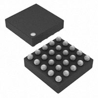
TPA2050D4
www.ti.com....................................................................................................................................................................................................... SLOS544 – JULY 2008
1.4 W/CH STEREO CLASS-D AUDIO SUBSYSTEM WITH DirectPath™ HEADPHONE
AMPLIFIER AND 2:1 INPUT MUX
FEATURES
1
• Stereo Class-D Amp:
– 1.4 W into 8 Ω from 5.0 V (10% THD + N)
– 1.25 W into 8 Ω from 5.0 V (1% THD + N)
• DirectPath™ Stereo Headphone Amplifier
– No Output Capacitors Required
• Gain Select for Headphone Amplifier
• Eight Programmable Maximum Headphone
Voltage Limits
• Two Single-Ended or One Differential Stereo
Input
• 2:1 Input MUX with Mode Control
• 32-Step Volume Control for Both Input
Channels
• Independent Shutdown for Headphone and
Class-D Amplifiers
• Short-Circuit and Thermal-Overload Protection
• ±8 kV HBM ESD Protection on Headphone
Outputs
• I2C™ Interface
• 25-Ball 2,61 mm × 2,61 mm WCSP
23
APPLICATIONS
•
•
•
•
Smart Phones / Cellular Phones
Laptop Computers
Portable Gaming
Portable Media Players
8 W Speaker
Codec
(MP3)
Right
(SE )
Left
(SE )
TPA2050D4
8 W Speaker
Stereo Class-D
plus
TM
DirectPath
FM Tuner
Right
(SE )
The TPA2050D4 features a stereo Class-D power
amplifier along with a stereo DirectPath™ headphone
amplifier. The TPA2050D4 has two stereo
single-ended (SE) inputs that can be configured as
one stereo differential input. Both input channels
have a 32-step volume control and the DirectPath
headphone amplifier has a 4-level gain control for
coarse volume adjustment. All amplifiers have output
short-circuit and thermal- overload protection.
The Class-D amplifiers deliver 1.25 W into 8 Ω at 1%
THD from a 5.0 V supply, and 700 mW from 3.6 V.
The DirectPath headphone amplifier features an
output voltage limiter to reduce the maximum output
power to one of seven possible limits. The voltage
limiter is programmed through the I2C interface.
DirectPath eliminates the need for external DCblocking output capacitors to the headphones. The
built-in charge pump creates a negative supply
voltage for the headphone amplifier, allowing a 0-V
DC bias at the output.
The DirectPath headphone amplifier gains are 0 dB
(default), –6 dB, –12 dB, and –20 dB, selected
through the I2C interface. This allows the headphone
volume to be different from the loudspeaker volume if
both are used simultaneously.
The TPA2050D4 has a 2:1 input MUX for audio
source selection. The MUX has mode control which
directs the input-to-output signal path. Mode and gain
controls operate from a 1.8 V compatible I2C
interface.
SIMPLIFIED SYSTEM BLOCK DIAGRAM
Left
(SE )
DESCRIPTION
Stereo
Headphone Jack
The voltage supply range for both the Class-D
amplifiers and the headphone charge pump is 2.5 V
to 5.5 V. The Class-D amplifiers use a combined 7
mA and the headphone amplifier uses 10 mA of
typical quiescent current. Total supply current
reduces to less than 2µA.
The TPA2050D4YZK is available in a 25-ball 2.61
mm × 2.61 mm WCSP package.
1
2
3
Please be aware that an important notice concerning availability, standard warranty, and use in critical applications of Texas
Instruments semiconductor products and disclaimers thereto appears at the end of this data sheet.
DirectPath is a trademark of Texas Instruments.
I2C is a trademark of NXP Semiconductors.
PRODUCTION DATA information is current as of publication date.
Products conform to specifications per the terms of the Texas
Instruments standard warranty. Production processing does not
necessarily include testing of all parameters.
Copyright © 2008, Texas Instruments Incorporated
�TPA2050D4
SLOS544 – JULY 2008....................................................................................................................................................................................................... www.ti.com
These devices have limited built-in ESD protection. The leads should be shorted together or the device placed in conductive foam
during storage or handling to prevent electrostatic damage to the MOS gates.
ORDERING INFORMATION
PACKAGED DEVICES (1)
PART NUMBER (2)
25-ball, 2,61 mm × 2,61 mm WCSP (+0.01/-0.09 mm tolerance)
TPA2050D4YZKR
25-ball, 2,61 mm × 2,61 mm WCSP (+0.01/-0.09 mm tolerance)
TPA2050D4YZKT
TA
–40°C to 85°C
(1)
(2)
For the most current package and ordering information, see the Package Option Addendum at the end of this document, or see the TI
Web site at www.ti.com.
The YZK packages are only available taped and reeled. The suffix R indicates a reel of 3000, the suffix T indicates a reel of 250.
DEVICE PINOUT
2
A1
A2
A3
A4
A5
VREF
INL_ 1
INR _1
DVDD
OUTL +
B1
B2
B3
B4
B5
CPP
INR _2
INL_2
RESET
OUTL–
C1
C2
C3
C4
C5
CPN
SDA
SCL
AGND
PGND
D1
D2
D3
D4
D5
HPVSS
GND
GND
AVDD
OUTR –
E1
E2
E3
E4
E5
HPRIGHT
VDDHP
HPLEFT
PVDD
OUTR +
Submit Documentation Feedback
Copyright © 2008, Texas Instruments Incorporated
Product Folder Link(s): TPA2050D4
�TPA2050D4
www.ti.com....................................................................................................................................................................................................... SLOS544 – JULY 2008
FUNCTIONAL BLOCK DIAGRAM
1 µF
VDD
VDD
1 µF
VREF
Bias Control
and Pop
Suppression
PGND
VDD
0.47 µF
LIN+
+
LIN–
–
HBridge
PWM
–60dB to +12dB
Volume
Control
RIN+
+
RIN–
–
Mode
Control
OUTL+
Oscillator
HBridge
PWM
0.47 µF
0.47 µF
OUTL–
OUTR–
OUTR+
PGND
VDDHP
HPLEFT
4-Level
Gain
Select
0.47 µF
VSS
VDDHP
DVDD
HPRIGHT
SDA
VSS
2
I C Interface
SCL
Headphone
Power
Limiter
Charge
Pump
RESET
CPP
VDDHP
CPN
1 µF
VSS
PGND
1 µF
Figure 1. Differential Input Mode
1 µF
VDD
VDD
1 µF
Bias Control
and Pop
Suppression
VREF
PWM
PGND
VDD
0.47 µF
LIN1
–60 dB to +12 dB
Volume Control
HBridge
PWM
Mode
Control
LIN2
OUTL+
Oscillator
HBridge
RIN1
0.47 µF
0.47 µF
OUTL–
OUTR–
OUTR+
PGND
VDDHP
–60 dB to +12 dB
Volume Control
HPLEFT
RIN2
4-Level
Gain
Select
0.47 µF
VSS
VDDHP
DVDD
HPRIGHT
SDA
VSS
2
I C Interface
SCL
Headphone
Power
Limiter
Charge
Pump
RESET
CPP
VDDHP
CPN
1 µF
VSS
PGND
1 µF
Figure 2. Single-Ended (SE) Input Mode
Submit Documentation Feedback
Copyright © 2008, Texas Instruments Incorporated
Product Folder Link(s): TPA2050D4
3
�TPA2050D4
SLOS544 – JULY 2008....................................................................................................................................................................................................... www.ti.com
TERMINAL FUNCTIONS
TERMINAL
INPUT/ OUTPUT/
POWER (I/O/P)
DESCRIPTION
NAME
BALL
WCSP
OUTL+
A5
O
Left speaker positive output; connect to + terminal of loudspeaker
DVDD
A4
P
I2C supply voltage; connect to 1.8V digital supply
INR_1
A3
I
Channel 1 right input (SE-In mode); Left– input (Diff-In mode); connect to ground through 0.47 µF
capacitor if unused
INL_1
A2
I
Channel 1 left input (SE-In mode); Left+ input (Diff-In mode); connect to ground through 0.47 µF
capacitor if unused
VREF
A1
I
1.65 V reference voltage; connect a 1 µF capacitor to ground
OUTL–
B5
O
Left speaker negative output; connect to negative terminal of loudspeaker
RESET
B4
I
Set to logic low to shut device down and return all I2C register to default state; I2C can only be
programmed once RESET returns to logic high
INL_2
B3
I
Channel 2 left input (SE-In mode); Right+ input (Diff-In mode); connect to ground through 0.47 µF
capacitor if unused
INR_2
B2
I
Channel 2 right input (SE-In mode); Right– input (Diff-In mode); connect to ground through 0.47 µF
capacitor if unused
CPP
B1
P
Charge pump flying capacitor positive terminal; connect positive side of capacitor between CPP and CPN
PGND
C5
P
Class-D ground; connect to ground
AGND
C4
P
Analog ground; connect to ground
SCL
C3
I/O
I2C clock input
SDA
C2
I/O
I2C data input
CPN
C1
P
Charge pump flying capacitor negative terminal; connect negative side of capacitor between CPP and
CPN
OUTR–
D5
O
Right speaker negative output; connect to negative terminal of loudspeaker
AVDD
D4
P
Supply voltage
GND
D3
I
Connect to ground
GND
D2
I
Connect to ground
HPVSS
D1
P
Negative supply generated by the charge pump; connect a 1µF capacitor to ground to reduce voltage
ripple
OUTR+
E5
O
Right speaker positive output; connect to positive terminal of loudspeaker
PVDD
E4
P
Supply voltage
HPLEFT
E3
O
Headphone left channel output
VDDHP
E2
P
Headphone charge pump supply voltage
HPRIGHT
E1
O
Headphone right channel output
4
Submit Documentation Feedback
Copyright © 2008, Texas Instruments Incorporated
Product Folder Link(s): TPA2050D4
�TPA2050D4
www.ti.com....................................................................................................................................................................................................... SLOS544 – JULY 2008
ABSOLUTE MAXIMUM RATINGS (1)
over operating free-air temperature range, TA = 25°C (unless otherwise noted)
Supply voltage,
VI
Input voltage
VALUE
UNIT
VDDHP, PVDD, AVDD
–0.3 to 6.0
V
DVDD
-0.3 to 3.6
V
INL_1, INL_2, INR_1, INR_2
–0.3 to VDD + 0.3
V
SDA, SCL, RESET
-0.3 to DVDD + 0.3
V
Output continuous total power dissipation
See Dissipation Rating
Table
TA
Operating free-air temperature range
–40 to 85
°C
TJ
Operating junction temperature range
–40 to 150
°C
Tstg
Storage temperature range
–65 to 150
°C
ESD
Electrostatic discharge,
HBM
OUTL+, OUTL–, OUTR+, OUTR–
2k
V
HPLEFT and HPRIGHT
8k
V
260
°C
Lead temperature 1,6 mm (1/16 inch) from case for 10 seconds
(1)
Stresses beyond those listed under absolute maximum ratings may cause permanent damage to the device. These are stress ratings
only, and functional operation of the device at these or any other conditions beyond those indicated under recommended operating
conditions is not implied. Exposure to absolute-maximum-rated conditions for extended periods may affect device reliability.
DISSIPATION RATINGS
PACKAGE
TA < 25°C
DERATING FACTOR
TA = 70°C
TA = 85°C
YZK (WCSP)
1.12 W
9 mW/°C
720 mW
585 mW
RECOMMENDED OPERATING CONDITIONS
over operating free-air temperature range (unless otherwise noted)
MIN
MAX
Class-D supply voltage, PVDD
2.5
5.5
V
Charge pump supply voltage, VDDHP
2.5
5.5
V
I2C supply voltage, DVDD
1.7
1.95
V
VIH
High-level input voltage
SDA, SCL, RESET
VIL
Low-level input voltage
SDA, SCL, RESET
TA
Operation free-air temperature
UNIT
1.3
V
0.3
V
85
°C
–40
ELECTRICAL CHARACTERISTICS
TA = 25°C (unless otherwise noted)
PARAMETER
TEST CONDITIONS
MIN
TYP MAX
UNIT
DC Power supply rejection ratio
(Class-D amplifiers)
VDD = 2.5 V to 5.5 V, Single-ended mode
48
75
dB
DC Power supply rejection ratio
(headphone amplifiers)
VDD = 2.5 V to 5.5 V, Single-ended mode
60
80
dB
High-level input current (SDA, SCL,
RESET)
1
µA
Low-level input current (SDA, SCL,
RESET)
1
µA
15.8
20
mA
7.5
10.5
mA
10
13.5
mA
0.15
2
µA
Supply current
VDD = 5.5 V, Class-D and Headphone ampifiers active, no load
VDD = 4.2 V, Class-D active, Headphone deactivated, no load
VDD = 4.2 V, Headphone active, Class-D deactivated, no load
VDD = 2.5 V to 5.5 V, SWS=1 or RESET ≤ 0.3 V (shutdown mode)
Submit Documentation Feedback
Copyright © 2008, Texas Instruments Incorporated
Product Folder Link(s): TPA2050D4
5
�TPA2050D4
SLOS544 – JULY 2008....................................................................................................................................................................................................... www.ti.com
TIMING CHARACTERISTICS
For I2C Interface Signals Over Recommended Operating Conditions (unless otherwise noted)
PARAMETER
fSCLN
Frequency, SCL
tW(H)
Pulse duration, SCL high
tW(L)
tsu1
TEST CONDITIONS
MIN
No wait states
TYP
MAX
UNIT
400
kHz
0.6
µs
Pulse duration, SCL low
1.3
µs
Setup time, SDA to SCL
100
ns
th1
Hold time, SCL to SDA
10
ns
t(buf)
Bus free time between stop and start condition
1.3
µs
tsu2
Setup time, SCL to start condition
0.6
µs
th2
Hold time, start condition to SCL
0.6
µs
tsu3
Setup time, SCL to stop condition
0.6
µs
Figure 3. SCL and SDA Timing
Figure 4. Start and Stop Conditions Timing
DEVICE RESET
Apply logic low to the RESET pin to deactivate the TPA2050D4 and return all I2C registers to their default state.
This clears the LIM_Lock bit to logic low, allowing changes to the headphone output limiter byte. Refer to the
Register Map section for a complete list of default states. The I2C registers cannot be programmed until RESET
returns to logic high. RESET requires a 1 ms minimum hold time at logic low for a valid reset command.
On power-up, ensure that the DVDD and VDDHP voltages have settled and DVDD is at least 1.7V before setting
RESET to logic high. The TPA2050D4 activates in soft shutdown mode, SWS bit at logic high.
6
Submit Documentation Feedback
Copyright © 2008, Texas Instruments Incorporated
Product Folder Link(s): TPA2050D4
�TPA2050D4
www.ti.com....................................................................................................................................................................................................... SLOS544 – JULY 2008
OPERATING CHARACTERISTICS
VDD = 3.6 V, TA = 25°C, RSPEAKER = 8 Ω + 33 µH, RHEADPHONES = 16 Ω, Volume = 6 dB, HP Gain = 0 dB, MODE[2:0] = 001
(single-ended mode)(unless otherwise noted)
PARAMETER
TEST CONDITIONS
MIN
TYP
MAX
UNIT
POWER AMPLIFIER
PO
Speaker output power
VOS
Offset Voltage
THD = 1%, VDD = 3.6 V, f = 1 kHz
700
mW
THD = 10%, VDD = 3.6 V, f = 1 kHz
860
mW
THD = 1%, VDD = 4.2 V, f = 1 kHz
940
VDD = 5.5 V, Volume = 0 dB
-13
Output impedance in shutdown
5
mW
13
2
mV
kΩ
SNR
Signal-to-noise ratio
PO = 600 mW;
En
Noise output voltage
Volume = 0 dB; A-weighted
19.4
µVRMS
THD+N
Total harmonic distortion plus noise
VDD = 5.0 V, PO = 1 W, f = 1 kHz
0.22
%
kSVR
AC-Power supply rejection ratio
Thermal shutdown
90
VDD = 3.6 V, PO = 0.6 W, f = 1 kHz
0.27
%
200 mVpp ripple, f = 217 Hz, Volume = 0 dB
-77.7
dB
200 mVpp ripple, f = 4 kHz, Volume = 0 dB
-60.3
dB
155
°C
35
°C
Threshold
Hysteresis
Output short-circuit protection
fCLK
Class-D switching frequency
ΔAV
Gain matching
dB
2.4
250
300
Between left and right channels
0.1
THD = 1%, VDD = 5.0 V, HP_Vout[2:0] = 000
145
THD = 1%, VDD = 3.0 V, HP_Vout[2:0] = 000
79
A
350
kHz
dB
HEADPHONE AMPLIFIER
PO
Headphone output power (1)
(Outputs in Phase)
VO
Maximum headphone output voltage
VOS
Offset Voltage
THD = 10 %, HP_VOUT[2:0] = 111
0.14
THD = 10 %, HP_VOUT[2:0] = 100
0.23
VDD = 5.5 V, Volume = 0 dB
-3.5
0.5
mW
VRMS
3.5
mV
30
Ω
SNR
Signal-to-noise ratio
PO = 50 mW;
90
dB
En
Noise output voltage
Volume = 0 dB; A-weighted, VDD = 5.0 V
12
µVRMS
THD+N
Total harmonic distortion plus noise(1)
Output impedance in shutdown
kSVR
AC-Power supply rejection ratio
PO = 20 mW into 16 Ω, VDD = 3.6 V, f = 1 kHz
0.005
PO = 50 mW into 32 Ω, VDD = 5.0 V, f = 1 kHz
0.0067
%
200 mVpp ripple, f = 217 Hz, Volume = 0 dB
-78.5
dB
200 mVpp ripple, f = 4 kHz, Volume = 0 dB
-75.6
dB
200
mA
300
kHz
0.1
dB
14.7
kΩ
1.65
V
8.25
ms
Output short-circuit protection
fOSC
Charge pump switching frequency
ΔAV
Gain matching
Between Left and Right channels
%
INPUT SECTION
RIN
Input impedance
Volume = 12 dB
VREF
Reference voltage
VDD = 3.6 V, all active modes
Start-up time from shutdown
(1)
11
Per output channel
Submit Documentation Feedback
Copyright © 2008, Texas Instruments Incorporated
Product Folder Link(s): TPA2050D4
7
�TPA2050D4
SLOS544 – JULY 2008....................................................................................................................................................................................................... www.ti.com
TEST SET-UP FOR GRAPHS
TPA2050D4
CI
+
Measurement
Output
–
IN+
OUT+
Load
CI
IN–
VDD
+
OUT–
30 kHz
Low-Pass
Filter
+
Measurement
Input
–
GND
1 mF
VDD
–
8
(1)
All measurements were taken with a 1-µF CI (unless otherwise noted.)
(2)
A 33-µH inductor was placed in series with the load resistor to emulate a small speaker for efficiency measurements.
(3)
The 30-kHz low-pass filter is required, even if the analyzer has an internal low-pass filter. An RC low-pass filter (1 kΩ
4.7 nF) is used on each output for the data sheet graphs.
Submit Documentation Feedback
Copyright © 2008, Texas Instruments Incorporated
Product Folder Link(s): TPA2050D4
�TPA2050D4
www.ti.com....................................................................................................................................................................................................... SLOS544 – JULY 2008
TYPICAL CHARACTERISTIC GRAPHS
CI= 1µF, Cbypass= 1µF
10
CIN = 1 µF
Gain = 6 dB
PO = 150 mW
RL = 8 Ω + 33 µH
VSupply = 3 V
SE Mode
0.01
DIFF Mode
0.001
20
100
1k
10k 20k
CIN = 1 µF
Gain = 6 dB
PO = 300 mW
RL = 8 Ω + 33 µH
VSupply = 3.6 V
1
0.1
SE Mode
0.01
DIFF Mode
0.001
20
100
f − Frequency − Hz
1k
10k 20k
0.001
20
100
1k
10k 20k
G003
TOTAL HARMONIC
DISTORTION+NOISE (HP)
vs
FREQUENCY
TOTAL HARMONIC
DISTORTION+NOISE (HP)
vs
FREQUENCY
TOTAL HARMONIC
DISTORTION+NOISE (HP)
vs
FREQUENCY
SE Mode
0.01
DIFF Mode
0.001
100
1k
10k 20k
THD+N − Total Harmonic Distortion + Noise − %
THD+N − Total Harmonic Distortion + Noise − %
DIFF Mode
G002
10
CIN = 1 µF
Gain = 6 dB/HP Gain = 0 dB
PO = 50 mW
RL = 16 Ω
VSupply = 3.6 V
1
0.1
SE Mode
0.01
DIFF Mode
0.001
20
100
1k
10k 20k
10
CIN = 1 µF
Gain = 6 dB/HP Gain = 0 dB
PO = 100 mW
RL = 16 Ω
VSupply = 5 V
1
0.1
DIFF Mode
0.01
SE Mode
0.001
20
100
1k
10k 20k
f − Frequency − Hz
f − Frequency − Hz
f − Frequency − Hz
G006
G005
G004
Figure 9.
Figure 10.
Figure 11.
TOTAL HARMONIC
DISTORTION+NOISE (HP)
vs
FREQUENCY
TOTAL HARMONIC
DISTORTION+NOISE (HP)
vs
FREQUENCY
TOTAL HARMONIC
DISTORTION+NOISE (HP)
vs
FREQUENCY
10
CIN = 1 µF
Gain = 6 dB/HP Gain = 0 dB
PO = 20 mW
RL = 32 Ω
VSupply = 3 V
0.1
SE Mode
0.01
DIFF Mode
0.001
100
1k
10k 20k
f − Frequency − Hz
THD+N − Total Harmonic Distortion + Noise − %
THD+N − Total Harmonic Distortion + Noise − %
0.01
Figure 8.
0.1
20
SE Mode
0.1
Figure 7.
CIN = 1 µF
Gain = 6 dB/HP Gain = 0 dB
PO = 35 mW
RL = 16 Ω
VSupply = 3 V
1
1
Figure 6.
10
20
CIN = 1 µF
Gain = 6 dB
PO = 600 mW
RL = 8 Ω + 33 µH
VSupply = 5 V
f − Frequency − Hz
G001
1
10
f − Frequency − Hz
THD+N − Total Harmonic Distortion + Noise − %
0.1
10
10
CIN = 1 µF
Gain = 6 dB/HP Gain = 0 dB
PO = 30 mW
RL = 32 Ω
VSupply = 3.6 V
1
0.1
DIFF Mode
0.01
SE Mode
0.001
20
100
1k
10k 20k
f − Frequency − Hz
G007
Figure 12.
THD+N − Total Harmonic Distortion + Noise − %
1
TOTAL HARMONIC
DISTORTION+NOISE (SP)
vs
FREQUENCY
THD+N − Total Harmonic Distortion + Noise − %
TOTAL HARMONIC
DISTORTION+NOISE (SP)
vs
FREQUENCY
THD+N − Total Harmonic Distortion + Noise − %
THD+N − Total Harmonic Distortion + Noise − %
TOTAL HARMONIC
DISTORTION+NOISE (SP)
vs
FREQUENCY
10
CIN = 1 µF
Gain = 6 dB/HP Gain = 0 dB
PO = 50 mW
RL = 32 Ω
VSupply = 5 V
1
0.1
DIFF Mode
0.01
SE Mode
0.001
20
100
1k
G008
Figure 13.
G009
Figure 14.
Submit Documentation Feedback
Copyright © 2008, Texas Instruments Incorporated
Product Folder Link(s): TPA2050D4
10k 20k
f − Frequency − Hz
9
�TPA2050D4
SLOS544 – JULY 2008....................................................................................................................................................................................................... www.ti.com
TYPICAL CHARACTERISTIC GRAPHS (continued)
CI= 1µF, Cbypass= 1µF
VSupply = 3 V
VSupply = 2.5 V
0.1
VSupply = 3.6 V
0.01
0.001
VSupply = 5 V
0.01
0.1
10
1
1
0.1
VSupply = 3.6 V
0.01
0.001
VSupply = 5 V
0.01
0.1
10
1
PO − Output Power − W
1
VSupply = 3.6 V
VSupply = 3 V
0.1
VSupply = 2.5 V
0.01
0.001
0.0001
0.001
0.01
1
0.1
PO − Output Power − W
G012
Figure 17.
TOTAL HARMONIC
DISTORTION+NOISE (HP)
vs
POWER
TOTAL HARMONIC
DISTORTION+NOISE (HP)
vs
POWER
TOTAL HARMONIC
DISTORTION+NOISE (HP)
vs
POWER
VSupply = 5 V
VSupply = 3.6 V
VSupply = 3 V
VSupply = 2.5 V
0.01
0.001
0.01
1
0.1
PO − Output Power − W
100
10
f = 1 kHz
Gain = 6 dB/HP = 0 dB
RL = 32 Ω
Stereo Differential
VSupply = 5 V
1
VSupply = 3.6 V
VSupply = 3 V
0.1
VSupply = 2.5 V
0.01
0.001
0.0001
0.001
0.01
1
0.1
PO − Output Power − W
G013
100
10
f = 1 kHz
Gain = 6 dB/HP = 0 dB
RL = 32 Ω
Stereo Single-Ended
1
VSupply = 3.6 V
VSupply = 3 V
0.1
VSupply = 2.5 V
0.01
0.001
0.0001
VSupply = 5 V
0.001
0.01
0.1
PO − Output Power − W
G014
1
G015
Figure 18.
Figure 19.
Figure 20.
SUPPLY RIPPLE REJECTION RATIO
(SP)
vs
FREQUENCY
SUPPLY RIPPLE REJECTION RATIO
(SP)
vs
FREQUENCY
SUPPLY RIPPLE REJECTION RATIO
(HP)
vs
FREQUENCY
0
0
0
−20
Gain = 0 dB
RL = 8 Ω + 33 µH
Stereo Differential
Input Level = 0.2 Vpp
−40
−60
VDD = 3 V
VDD = 2.5 V
−80
−100
VDD = 5 V
VDD = 3.6 V
−120
20
100
1k
10k 20k
f − Frequency − Hz
−20
Gain = 0 dB
RL = 8 Ω + 33 µH
Stereo Single-Ended
Input Level = 0.2 Vpp
−40
−60
VDD = 5 V
VDD = 3 V
−80
VDD = 3.6 V
−100
VDD = 2.5 V
−120
20
100
1k
10k 20k
f − Frequency − Hz
G016
Figure 21.
10
f = 1 kHz
Gain = 6 dB/HP = 0 dB
RL = 16 Ω
Stereo Differential
VSupply = 5 V
G011
SRRR − Supply Ripple Rejection Ratio − dB
THD+N − Total Harmonic Distortion + Noise − %
VSupply = 2.5 V
10
Figure 16.
1
0.001
0.0001
VSupply = 3 V
100
Figure 15.
f = 1 kHz
Gain = 6 dB/HP = 0 dB
RL = 16 Ω
Stereo Single-Ended
0.1
10
f = 1 kHz
Gain = 6 dB
RL = 8 Ω + 33 µH
Stereo Single-Ended
G010
100
10
100
THD+N − Total Harmonic Distortion + Noise − %
1
THD+N − Total Harmonic Distortion + Noise − %
10
TOTAL HARMONIC
DISTORTION+NOISE (HP)
vs
POWER
THD+N − Total Harmonic Distortion + Noise − %
f = 1 kHz
Gain = 6 dB
RL = 8 Ω + 33 µH
Stereo Differential
THD+N − Total Harmonic Distortion + Noise − %
100
PO − Output Power − W
SRRR − Supply Ripple Rejection Ratio − dB
TOTAL HARMONIC
DISTORTION+NOISE (SP)
vs
POWER
SRRR − Supply Ripple Rejection Ratio − dB
THD+N − Total Harmonic Distortion + Noise − %
TOTAL HARMONIC
DISTORTION+NOISE (SP)
vs
POWER
−20
Gain = 0 dB/HP Gain = 0 dB
RL = 32 Ω
Stereo Differential
Input Level = 0.2 Vpp
−40
−60
VDD = 2.5 V
VDD = 3 V
−80
−100
VDD = 5 V
VDD = 3.6 V
−120
20
100
1k
Figure 22.
Submit Documentation Feedback
10k 20k
f − Frequency − Hz
G017
G018
Figure 23.
Copyright © 2008, Texas Instruments Incorporated
Product Folder Link(s): TPA2050D4
�TPA2050D4
www.ti.com....................................................................................................................................................................................................... SLOS544 – JULY 2008
TYPICAL CHARACTERISTIC GRAPHS (continued)
CI= 1µF, Cbypass= 1µF
EFFICIENCY (SP)
vs
OUTPUT POWER PER CHANNEL
0
80
VDD = 2.5 V
−60
VDD = 3.6 V
−80
VDD = 3.6 V
60
50
VDD = 3 V
40
30
f = 1 kHz
Gain = 6 dB
RL = 8 Ω + 33 µH
Stereo Single-Ended
20
−100
VDD = 5 V
VDD = 3 V
−120
20
10
100
1k
0.25
VDD = 3.6 V
0.20
VDD = 2.5 V
0.15
0.10
VDD = 5 V
VDD
VDD= =3 3V V
0.00
0.0
10k 20k
0.30
0.05
0
0.5
1.0
1.5
PO − Output Power (Per Channel) − W
G019
0.0
0.5
1.0
1.5
2.0
2.5
PO − Output Power − W
G020
3.0
G021
Figure 24.
Figure 25.
Figure 26.
TOTAL POWER DISSIPATION (HP)
vs
TOTAL OUTPUT POWER
TOTAL POWER DISSIPATION (HP)
vs
TOTAL OUTPUT POWER
OUTPUT POWER PER CHANNEL (SP)
vs
SUPPLY VOLTAGE
0.6
PD − Total Power Dissipation − W
0.8
VDD = 3 V
0.7
VDD = 5 V
0.6
VDD = 3.6 V
0.5
0.4
0.3
VDD = 2.5 V
0.2
Gain = 6 dB/HP Gain = 0 dB
RL = 16 Ω, f = 1 kHz
Stereo Single-Ended
Pdiss = PdissL + PdissR
0.1
0.0
0.0
0.1
0.2
0.3
0.4
PO − Output Power − W
1.6
Gain = 6 dB/HP Gain = 0 dB
RL = 32 Ω, f = 1 kHz
Stereo Single-Ended
Pdiss = PdissL + PdissR
0.5
0.4
VDD = 5 V
VDD = 3.6 V
0.3
0.2
VDD = 3 V
0.1
f = 1 kHz
Gain = 6 dB
RL = 8 Ω + 33 µH
Stereo Single-Ended
1.4
PO − Output Power − W
0.9
1.2
THD = 10%
1.0
0.8
0.6
THD = 1%
0.4
0.2
VDD = 2.5 V
0.0
0.00
0.5
0.0
0.05
0.10
0.15
0.20
0.25
PO − Output Power − W
G022
2.5
3.0
3.5
4.0
4.5
5.0
VDD − Supply Voltage − V
G023
5.5
G024
Figure 27.
Figure 28.
Figure 29.
OUTPUT POWER PER CHANNEL (HP)
vs
SUPPLY VOLTAGE
OUTPUT POWER PER CHANNEL (HP)
vs
SUPPLY VOLTAGE
COMMON-MODE REJECTION RATIO
(SP)
vs
FREQUENCY
0.12
0.20
THD = 10%
PO − Output Power − W
0.10
0.15
0.10
THD = 1%
f = 1 kHz
Gain = 6 dB/HP Gain = 0 dB
RL = 16 Ω
Stereo Single-Ended
0.05
THD = 10%
0.08
THD = 1%
0.06
0.04
f = 1 kHz
Gain = 6 dB/HP Gain = 0 dB
RL = 32 Ω
Stereo Single-Ended
0.02
0.00
CMRR − Common-Mode Rejection Ratio − dB
PD − Total Power Dissipation − W
VDD = 5 V
VDD = 2.5 V
70
−40
f = 1 kHz
Gain = 6 dB
RL = 8 Ω + 33 µH
Stereo Single-Ended
Pdiss = PdissL + PdissR
0.35
PD − Power Dissipation − W
−20
0.40
90
f − Frequency − Hz
PO − Output Power − W
TOTAL POWER DISSIPATION (SP)
vs
TOTAL OUTPUT POWER
100
Gain = 0 dB/HP Gain = 0 dB
RL = 32 Ω
Stereo Single-Ended
Input Level = 0.2 Vpp
Efficiency − %
SRRR − Supply Ripple Rejection Ratio − dB
SUPPLY RIPPLE REJECTION RATIO
(HP)
vs
FREQUENCY
0.00
2.5
3.0
3.5
4.0
4.5
VDD − Supply Voltage − V
5.0
5.5
G025
Figure 30.
2.5
3.0
3.5
4.0
4.5
5.0
VDD − Supply Voltage − V
Figure 31.
5.5
G026
0
−10
−20
Gain = 6 dB
Input Level = 0.2 Vpp
RL = 8 Ω + 33 µH
VDD = 3.6 V
−30
−40
−50
Left Speaker
−60
−70
−80
20
100
1k
G027
Figure 32.
Submit Documentation Feedback
Copyright © 2008, Texas Instruments Incorporated
Product Folder Link(s): TPA2050D4
10k 20k
f − Frequency − Hz
11
�TPA2050D4
SLOS544 – JULY 2008....................................................................................................................................................................................................... www.ti.com
TYPICAL CHARACTERISTIC GRAPHS (continued)
CI= 1µF, Cbypass= 1µF
CROSSTALK (SP)
vs
FREQUENCY
CROSSTALK (HP)
vs
FREQUENCY
0
0
Gain = 6 dB/HP Gain = 0 dB
Input Level = 0.2 Vpp
RL = 32 Ω
VDD = 3.6 V
−10
−20
−20
−40
−30
−40
−50
Left Headphone
Power = 0.25 W
RL = 8 Ω + 33 µH
VDD = 3.6 V
Stereo Single-Ended
−60
Left to Right
−80
Left to Right
−60
−80
Right to Left
−100
−120
−70
Right to Left
−80
20
100
1k
−140
20
10k 20k
100
1k
−120
20
10k 20k
G029
G030
Figure 35.
SUPPLY CURRENT
vs
SUPPLY VOLTAGE
SUPPLY CURRENT
vs
SUPPLY VOLTAGE
SUPPLY CURRENT
vs
SUPPLY VOLTAGE
50
50
Gain = 6 dB
HP Load = 32 Ω
RL = 8 Ω + 33 µH
Headphone Enabled Only
30
25
20
15
10
5
40
35
30
25
20
15
10
3.0
3.5
4.0
4.5
VDD − Supply Voltage − V
5.0
5.5
G031
Figure 36.
35
30
25
20
15
10
0
0
2.5
40
5
5
0
Gain = 6 dB
HP Load = 32 Ω
RL = 8 Ω + 33 µH
Speaker and Headphone Enabled
45
IDD − Supply Current − mA
45
IDD − Supply Current − mA
35
10k 20k
Figure 34.
Gain = 6 dB
HP Load = 32 Ω
RL = 8 Ω + 33 µH
Speaker Enabled Only
40
1k
f − Frequency − Hz
Figure 33.
50
45
100
f − Frequency − Hz
G028
IDD − Supply Current − mA
−40
−100
−60
f − Frequency − Hz
12
Power = 35 mW
RL = 32 Ω
VDD = 3.6 V
Stereo Single-Ended
−20
Crosstalk − dB
0
Crosstalk − dB
CMRR − Common-Mode Rejection Ratio − dB
COMMON-MODE REJECTION RATIO
(HP)
vs
FREQUENCY
2.5
3.0
3.5
4.0
4.5
5.0
VDD − Supply Voltage − V
Figure 37.
Submit Documentation Feedback
5.5
2.5
3.0
3.5
4.0
4.5
VDD − Supply Voltage − V
G032
5.0
5.5
G033
Figure 38.
Copyright © 2008, Texas Instruments Incorporated
Product Folder Link(s): TPA2050D4
�TPA2050D4
www.ti.com....................................................................................................................................................................................................... SLOS544 – JULY 2008
TYPICAL CHARACTERISTIC GRAPHS (continued)
CI= 1µF, Cbypass= 1µF
SPEAKER OUTPUT - STARTUP
SPEAKER OUTPUT - SHUTDOWN
2.0
2.0
SDA
1.5
1.0
V − Voltage − V
1.0
V − Voltage − V
SDA
1.5
0.5
SPKR Output
0.0
−0.5
SPKR Output
0.5
0.0
−0.5
−1.0
0
2
4
6
8
10
12
14
16
18
−1.0
0.0 0.5 1.0 1.5 2.0 2.5 3.0 3.5 4.0 4.5 5.0
20
t − Time − ms
t − Time − ms
G034
G035
Figure 39.
Figure 40.
HEADPHONE OUTPUT - STARTUP FILTER
HEADPHONE OUTPUT - SHUTDOWN FILTER
2.0
2.0
SDA
1.5
1.5
1.0
V − Voltage − V
1.0
V − Voltage − V
SDA
0.5
SPKR Output
0.0
SPKR Output
0.5
0.0
−0.5
−0.5
−1.0
0
2
4
6
8
10
12
14
16
18
20
−1.0
0.0 0.5 1.0 1.5 2.0 2.5 3.0 3.5 4.0 4.5 5.0
t − Time − ms
t − Time − ms
G037
G036
Figure 41.
Figure 42.
Submit Documentation Feedback
Copyright © 2008, Texas Instruments Incorporated
Product Folder Link(s): TPA2050D4
13
�TPA2050D4
SLOS544 – JULY 2008....................................................................................................................................................................................................... www.ti.com
DETAILED DESCRIPTION
GENERAL I2C OPERATION
The I2C bus employs two signals, SDA (data) and SCL (clock), to communicate between integrated circuits in a
system. The bus transfers data serially one bit at a time. The address and data 8-bit bytes are transferred most
significant bit (MSB) first. In addition, each byte transferred on the bus is acknowledged by the receiving device
with an acknowledge bit. Each transfer operation begins with the master device driving a start condition on the
bus and ends with the master device driving a stop condition on the bus. The bus uses transistions on the data
terminal (SDA) while the clock is at logic high to indicate start and stop conditions. A high-to-low transistion on
SDA indicates a start and a low-to-high transistion indicates a stop. Normal data-bit transistions bust occur within
the low time of the clock period. Figure 43 shows a typical sequence. The master generates the 7-bit slave
address and the read/write (R/W) bit to open communication with another device and then waits for an
acknowledge condition. The TPA2050D4 holds SDA low during the acknowledge clock period to indicate
acknowledgment. When this occurs, the master transmits the next byte of the sequence. Each device is
addressed by a unique 7-bit slave address plus R/W bit (1 byte). All compatible devices share the same signals
via a bidirectional bus using a wired-AND connection.
An external pull-up resistor must be used for the SDA and SCL signals to set the logic high level for the bus.
When the bus level is 5 V, use pull-up resistors between 1 kΩ and 2 kΩ.
Figure 43. Typical I2C Sequence
There is no limit on the number of bytes that can be transmitted between start and stop conditions. When the last
word transfers, the master generates a stop condition to release the bus. Figure 43 shows a generic data
transfer sequence.
SINGLE AND MULTI-BYTE TRANSFERS
The serial control interface supports both single-byte and multi-byte read/write operations for all registers. During
multi-byte reads, the TPA2050D4 responds with data, one byte at a time, starting at the register assigned
provided the master devices continues to respond with acknowledgements.
The TPA2050D4 supports sequential I2C addressing. For write transactions, if a register is issued followed by
data for that register and all the remaining registers that follow, a sequential I2C write transaction has occurred.
For I2C sequential write transactions, the register issued then serves as the starting point and the amount of data
subsequently transmitted, before a stop or start is transmitted, determines how many registers are written to.
14
Submit Documentation Feedback
Copyright © 2008, Texas Instruments Incorporated
Product Folder Link(s): TPA2050D4
�TPA2050D4
www.ti.com....................................................................................................................................................................................................... SLOS544 – JULY 2008
SINGLE-BYTE WRITE
As shown in Figure 44, a single-byte data write transfer begins with the master device transmitting a start
condition followed by the I2C device address and the read/write bit. The read/write bit determines the direction of
the data transfer. For a write data transfer, the read/write bit must be set to 0. After receiving the correct I2C
device address and the read/write bit, the TPA2050D4 responds with an acknowledge bit. Next, the master
transmits the register byte corresponding to the TPA2050D4 internal memory address being accessed. After
receiving the regitster byte, the TPA2050D4 again responds with an acknowledge bit. Finally, the master device
transmits a stop condition to complete the single-byte data write transfer.
Figure 44. Single-Byte Write Transfer
MULTI-BYTE WRITE AND INCREMENTAL MULTI-BYTE WRITER
A multiple-byte data write transfer is identical to a single-byte data write transfer with the exception that multiple
data bytes are transmitted by the master device to the TPA2050D4 as shown in Figure 45. After receiving each
data byte, the TPA2050D4 responds with an acknowledge bit.
Figure 45. Multiple-Byte Write Transfer
SINGLE-BYTE READ
As shown in Figure 46, a single-byte data read transfer begins with the master device transmitting a start
condition followed by the I2C device address and the read/write bit. For the data read transfer, both a write
followed by a read are actually done. Initially, a write is done to transfer the address byte of the internal memory
address to be read. As a result, the read/write bit is set to a 0.
After receiving the TPA2050D4 address and the read/write bit, the TPA2050D4 responds with an acknowledge
bit. The master then sends the internal memory address byte, after which the TPA2050D4 issues an
acknowledge bit. The master device transmits another start condition followed by the TPA2050D4 address and
the read/write bit again. This time, the read/write bit is set to 1, indicating a read transfer. Next, the TPA2050D4
transmits the data byte from the memory address being read. After receiving the data byte, the master device
transmits a notacknowledge followed by a stop condition to complete the single-byte data read transfer.
Figure 46. Single-Byte Read Transfer
Submit Documentation Feedback
Copyright © 2008, Texas Instruments Incorporated
Product Folder Link(s): TPA2050D4
15
�TPA2050D4
SLOS544 – JULY 2008....................................................................................................................................................................................................... www.ti.com
MULTI-BYTE READY
A multiple-byte data read transfer is identical to a single-byte read transfer except that multiple data bytes are
transmitted by the TPA2050D4 to the master device as shown in Figure 47. With the exception of the last data
byte, the master device responds with an acknowledge bit after receiving each data byte.
Figure 47. Multi-Byte Read Transfer
REGISTER MAPS
REGISTER
BIT 7
BIT 6
BIT 5
BIT 4
BIT 3
BIT 2
BIT 1
BIT 0
1
Reserved
Reserved
Reserved
PAL_Fault
PAR_Fault
HPL_Fault
HPR_Fault
Thermal
2
Reserved
Reserved
Reserved
SWS
HPL_Enable
HPR_Enable
PA_Enable
Reserved
3
LIM_Lock
Reserved
Reserved
Reserved
Reserved
Mode[2]
Mode[1]
Mode[0]
4
Reserved
Reserved
Reserved
Reserved
Reserved
Reserved
Reserved
Reserved
5
Reserved
Reserved
Reserved
ST1_Vol[4]
ST1_Vol[3]
ST1_Vol[2]
ST1_Vol[1]
ST1_Vol[0]
6
Reserved
Reserved
Reserved
ST2_Vol[4]
ST2_Vol[3]
ST2_Vol[2]
ST2_Vol[1]
ST2_Vol[0]
7
Reserved
Reserved
Reserved
HP_Vout[2]
HP_Vout[1]
HP_Vout[0]
HP_Gain[1]
HP_Gain[0]
The TPA2050D4 I2C address is 0xE0 (binary 11100000) for writing and 0xE1 (binary 11100001) for reading.
Refer to the General I2C Operation section for more details.
Bits labeled Reserved are reserved for future enhancements. They may not be written to as it may change the
function of the device. If read, these bits may assume any value.
Any register above address 0x07 is reserved for testing and should not be written to because it may change the
function of the device. If read, these bits may assume any value.
Fault Register (Address: 1)
BIT
7
6
5
4
3
2
1
0
Function
Reserved
Reserved
Reserved
PAL_Fault
PAR_Fault
HPL_Fault
HPR_Fault
Thermal
Reset Value
0
0
0
0
0
0
0
0
Reserved
These bits are reserved for future enhancements. They will not change state if programmed. If
read these bits may assume any value.
PAL_Fault
Logic high indicates an over-current event has occurred on the Class-D left channel output. This
bit is clear-on-write. Only logic low can be written to this bit.
PAR_Fault
Logic high indicates an over-current event has occurred on the Class-D right channel output.
This bit is clear-on-write. Only logic low can be written to this bit.
HPL_Fault
Logic high indicates an over-current event has occurred on the headphone left channel output.
This bit is clear-on-write. Only logic low can be written to this bit.
HPR_Fault
Logic high indicates an over-current event has occurred on the headphone right channel output.
This bit is clear-on-write. Only logic low can be written to this bit.
Thermal
Logic high indicates thermal shutdown activated. Bit automatically clears when the thermal
condition lowers past the hysteresis threshold.
16
Submit Documentation Feedback
Copyright © 2008, Texas Instruments Incorporated
Product Folder Link(s): TPA2050D4
�TPA2050D4
www.ti.com....................................................................................................................................................................................................... SLOS544 – JULY 2008
Power Management Register (Address: 2)
BIT
7
6
5
4
3
2
1
0
Function
Reserved
Reserved
Reserved
SWS
HPL_Enable
HPR_Enable
PA_Enable
Reserved
Reset Value
0
0
0
1
0
0
0
0
Reserved
These bits are reserved for future enhancements. They will not change state if programmed. If
read these bits may assume any value.
SWS
Software shutdown. Set to logic high to deactivate the TPA2050D4. Logic low reactivates the
charge pump and input amplifiers; enable headphone and Class-D amplifiers using HPL_Enable,
HPR_Enable, and PA_Enable. Default on turn-on is SWS logic high.
HPL_Enable Headphone left channel enable. Set to logic low to deactivate left channel.
HPR_Enable Headphone right channel enable. Set to logic low to deactivate right channel.
PA_Enable
Class-D power amplifier enable. Set to logic low to deactivate both left and right Class-D power
amplifiers.
Mux Output Control Register (Address: 3)
BIT
7
6
5
4
3
2
1
0
Function
LIM_Lock
Reserved
Reserved
Reserved
Reserved
Mode[2]
Mode1]
Mode[0]
Reset Value
0
0
0
0
0
0
0
1
Reserved
These bits are reserved for future enhancements. They will not change state if programmed. If
read these bits may assume any value.
LIM_Lock
Limiter change lockout. Set bit to logic high to prevent any changes to the HP_Vout[2:0] and
LIM_Lock bits. The LIM_Lock bit can only be returned to 0 by applying logic low to the RESET
pin or powering down VDD.
Mode[2:0]
Sets mux output mode. Refer to Modes of Operation section for details. Default mode is 001
(Stereo 1 Input mode) on power-up.
Reserved Control Register (Address: 4)
BIT
7
6
5
4
3
2
1
0
Function
Reserved
Reserved
Reserved
Reserved
Reserved
Reserved
Reserved
Reserved
Reset Value
0
0
0
1
0
0
1
1
Reserved
These bits are reserved for future enhancements. They will not change state if programmed. If
read these bits may assume any value.
Stereo Input 1 Volume Control Register (Address: 5)
BIT
7
6
5
4
3
2
1
0
Function
Reserved
Reserved
Reserved
ST1_Vol[4]
ST1_Vol[3]
ST1_Vol[2]
ST1_Vol[1]
ST1_Vol[0]
Reset Value
0
0
0
1
0
0
1
1
Reserved
These bits are reserved for future enhancements. They will not change state if programmed. If
read these bits may assume any value.
ST1_Vol[4:0] Five-bit volume control for Stereo Input 1 in single-ended input mode and stereo input pair in
differential input mode. 11111 sets device to its highest gain (+12 dB); 00000 sets device to its
lowest gain (–60 dB). Default setting on power-up is 10011 (+0 dB).
Submit Documentation Feedback
Copyright © 2008, Texas Instruments Incorporated
Product Folder Link(s): TPA2050D4
17
�TPA2050D4
SLOS544 – JULY 2008....................................................................................................................................................................................................... www.ti.com
Stereo Input 2 Volume Control Register (Address: 6)
BIT
7
6
5
4
3
2
1
0
Function
Reserved
Reserved
Reserved
ST2_Vol[4]
ST2_Vol[3]
ST2_Vol[2]
ST2_Vol[1]
ST2_Vol[0]
Reset Value
0
0
0
1
0
0
1
1
Reserved
These bits are reserved for future enhancements. They will not change state if programmed. If
read these bits may assume any value.
ST2_Vol[4:0] Five-bit volume control for Stereo Input 2. 11111 sets device to its highest gain (+12 dB); 00000
sets device to its lowest gain (–60 dB). Default setting on power-up is 10011 (+0 dB).
Headphone Output Control Register (Address: 7)
BIT
7
6
5
4
3
2
1
0
Function
Reserved
Reserved
Reserved
HP_Vout[2]
HP_Vout[1]
HP_Vout[0]
HP_Gain[1]
HP_Gain[0]
Reset Value
0
0
0
0
0
0
0
0
Reserved
These bits are reserved for future enhancements. They will not change state if programmed.
If read these bits may assume any value.
HP_Vout[2:0]
Headphone output voltage limiter. Sets the maximum output voltage / power to the
headphones.
HP_Gain[1:0]
Headphone gain select. Sets the gain of the headphone output amplifiers.
18
Submit Documentation Feedback
Copyright © 2008, Texas Instruments Incorporated
Product Folder Link(s): TPA2050D4
�TPA2050D4
www.ti.com....................................................................................................................................................................................................... SLOS544 – JULY 2008
MODES OF OPERATION
The TPA2050D4 has several operating modes for single-ended and differential inputs. Stereo 1 refers to the
LIN_1 and RIN_1 input pair; Stereo 2 refers to the LIN_2 and RIN_2 input pair.
Mux Output Mode
The input mux selects which device input is directed to both the Class-D and headphone amplifiers. Mux
summing and output are after the channel volume controls, as shown in the Simplified Functional Diagram.
Program the mux mode using the Mode[2:0] bits in Mux Output Control (Register 3, Bits 0–2). Select the
appropriate mode according to the table below.
MODE
BYTE:
MODE[2:0]
MUX OUTPUT
MUX MODE
LEFT
MUX OUTPUT DESCRIPTION
RIGHT
000
Reserved
Mute
Mute
No audio available at mux output
001
Stereo 1 Input
LIN_1
RIN_1
LIN_1 and RIN_1 stereo single-ended input
010
Stereo 2 Input
LIN_2
RIN_2
LIN_2 and RIN_2 stereo single-ended input
011
Stereo Differential
LIN_1–RIN_1
LIN_2–RIN_2
LIN_1 and RIN_1 compose the left channel; LIN_2 and
RIN_2 compose the right channel
100
Mono Differential
(LIN_1–RIN_1) +
(LIN_2–RIN_2)
(LIN_1–RIN_1) +
(LIN_2–RIN_2)
Left and right differential inputs summed and directed to
left and right mux output
101
Stereo 1 (monomode) LIN_1 + RIN_1
LIN_1 + RIN_1
LIN_1 + RIN_1 distributed to both left and right inputs of
the headphone and Class-D amplifiers
110
Stereo 2 (monomode) LIN_2 + RIN_2
LIN_2 + RIN_2
LIN_2 + RIN_2 distributed to both left and right inputs of
the headphone and Class-D amplifiers
111
Mute
Mute
All inputs muted; no audio available at mux output
Mute
Differential Input Mode
The LIN_1 and RIN_1 input pair and the LIN_2 and RIN_2 input pair are configurable as either single-ended or
differential inputs. Differential transmission between an audio source and the TPA2050D4 input improves system
noise rejection when compared to single-ended transmission.
In differential input modes, connect the Left+ and Left– source signal to LIN_1 and RIN_1, respectively; connect
Right+ and Right– to LIN_2 and RIN_2, respectively. Single-ended input modes allow selection between two
stereo sources. Differential input modes allow connection to only one stereo source.
START-UP SEQUENCING AND SHUTDOWN CONTROL
For correct start up with no turn-on pop, apply PVDD and VDDHP before applying DVDD while keeping RESET
at logic low. Once DVDD has settled to a minimum of 1.7 V, set RESET to logic high to complete the start-up
sequence. The TPA2050D4 starts up in soft shutdown mode with the SWS bit (Register 2, Bit 4) at logic high.
The stereo Class-D power amplifiers, left headphone amplifier, and right headphone amplifier each have their
own enable bits within the Power Management byte (Register 2, Bits 3–1). Set the corresponding bit to logic high
to enable these amplifiers. Disabling an amplifier mutes its output and reduces supply current. Set SWS to logic
high to deactivate all sections except the I2C interface, reducing total supply current to 2 µA,max.
Set RESET to logic low to deactivate all sections including the I2C interface. The I2C registers cannot be
programmed while RESET remains at logic low. Refer to the Headphone Output Limiter Lockout section for more
details on using RESET.
All register contents are maintained provided the supply voltage is not powered down and RESET remains at
logic high. On deactivation of DVDD or PVDD, or on RESET set to logic low, all information programmed into the
registers by the user is lost, returning to their default state once power is reapplied.
Submit Documentation Feedback
Copyright © 2008, Texas Instruments Incorporated
Product Folder Link(s): TPA2050D4
19
�TPA2050D4
SLOS544 – JULY 2008....................................................................................................................................................................................................... www.ti.com
Class-D Output Amplifiers
To enable both Class-D power amplifiers, set the PA_Enable bit (Register 2, Bit 1) to logic high. The left and
right channel Class-D outputs cannot be separately activated. Total Class-D section typical current is 7 mA when
active and less than 1 µA when deactivated.
All Class-D outputs have short-circuit current protection and thermal overload protection. The PAL_Fault and
PAR_Fault bits (Register 1, Bits 4 and 3) indicate an over-current event on the left and right Class-D channel
outputs. These bits are clear-on-write; only logic low can be written.
The Thermal bit (Register 1, Bit 1) goes to logic high if a thermal shutdown event occurs. It returns to logic low
once the device temperature returns below 150°C.
DirectPath Headphone Amplifier
Set the HPL_Enable bit (Register 2, Bit 3) to logic high to enable the headphone left output and the HPR_Enable
bit (Register 2, Bit 2) to logic high to enable the headphone right output. The headphone amplifier draws 10 mA
of typical supply current with both left and right outputs active and less than 1 µA when deactivated.
The HPL_Fault and HPR_Fault bits (Register 1, Bits 2 and 1) indicate an over-current event on the left and right
headphone outputs. These bits are clear-on-write; only logic low can be written.
HEADPHONE OUTPUT LIMITER LOCKOUT
Setting the LIM_Lock bit (Register 3, Bit 7) to logic high prevents any register changes to the HP_Vout byte
(Register 7, Bits 4-2) and the LIM_Lock bit itself. The LIM_Lock bit will remain locked at logic high until the power
supply is deactivated or logic low is applied to the RESET pin. All volume control, mux modes and shutdown
registers remain writable regardless of LIM_Lock status.
MAXIMUM HEADPHONE POWER REGULATOR
The HP_Vout byte (Register 7, Bits 4-2) sets the maximum output voltage from the headphone amplifiers. This is
useful for limiting the maximum output power to the headphones. The HP_Vout byte sets the internally regulated
supply voltage to the headphone amplifiers according to the table below. The table also shows the equivalent
10% THD output into 16Ω and 32Ω loads.
(1)
MAX HEADPHONE
OUTPUT BYTE: HP_VOUT[2:0]
VOUT,MAX
POUT,MAX INTO 16Ω
(10% THD)
POUT,MAX INTO 32Ω
(10% THD)
000
±VDDHP (1)
130 mW (at VDDHP = 3.6 V)
65 mW (at VDDHP = 3.6 V)
001
±1.13 V
40 mW
20 mW
010
±0.54 V
9 mW
4.5 mW
011
±0.38 V
4.5 mW
2.3 mW
100
±0.315 V
3.1 mW
1.6 mW
101
±0.253 V
2.0 mW
1.0 mW
110
±0.227 V
1.6 mW
0.8 mW
111
±0.196 V
1.2 mW
0.6 mW
With no load. Maximum output voltage decreases as load resistance decreases.
HEADPHONE GAIN VALUES
For the DirectPath headphone amplifier, left and right output channels
HEADPHONE GAIN REGISTER BYTE:
HP_GAIN[1:0]
20
NOMINAL GAIN
00
0 dB
01
–6 dB
10
–12 dB
11
–20 dB
Submit Documentation Feedback
Copyright © 2008, Texas Instruments Incorporated
Product Folder Link(s): TPA2050D4
�TPA2050D4
www.ti.com....................................................................................................................................................................................................... SLOS544 – JULY 2008
INPUT VOLUME CONTROL
The TPA2050D4 has two independent volume controls: One for the STEREO1 input pair (LIN_1 and RIN_1), and
one for the STEREO2 input pair (LIN_2 and RIN_2). Each has 5-bit (32-step) resolution and are audio tapered;
gain step changes are smaller at higher gain settings. The volume control range is –60 dB to +12 dB.
The Stereo Input 1 volume control byte is located at Register 5, Bits 4–0. The Stereo Input 2 volume control byte
is at Register 6, Bits 4–0. Gain matching between the left and right channels for STEREO1 and STEREO2 is
within 0.1 dB. In differential input mode, the Stereo Input 1 byte (Register 5) controls left and right channel gain.
The input impedance to the TPA2050D4 decreases as channel gain increases. See the Operating
Characteristics section for specifications. Values listed in Audio Taper Gain Values table are nominal values.
AUDIO TAPER GAIN VALUES
For input channel volume controls
VOLUME CONTROL
REGISTER BYTE: VOL[4:0]
NOMINAL GAIN
VOLUME CONTROL
REGISTER BYTE: VOL[4:0]
NOMINAL GAIN
00000
–60 dB
10000
–3.0 dB
00001
–48 dB
10001
–2.0 dB
00010
–43 dB
10010
–1.0 dB
00011
–38 dB
10011
+0 dB
00100
–33 dB
10100
+1.0 dB
00101
–29 dB
10101
+2.0 dB
00110
–25 dB
10110
+3.0 dB
00111
–21 dB
10111
+4.0 dB
01000
–17 dB
11000
+5.0 dB
01001
–15 dB
11001
+6.0 dB
01010
–13 dB
11010
+7.0 dB
01011
–11 dB
11011
+8.0 dB
01100
–9.0 dB
11100
+9.0 dB
01101
–7.5 dB
11101
+10 dB
01110
–6.0 dB
11110
+11.0 dB
01111
–4.5 dB
11111
+12.0 dB
Submit Documentation Feedback
Copyright © 2008, Texas Instruments Incorporated
Product Folder Link(s): TPA2050D4
21
�TPA2050D4
SLOS544 – JULY 2008....................................................................................................................................................................................................... www.ti.com
DECOUPLING CAPACITOR (CS)
The TPA2050D4 is a high-performance Class-D audio amplifier that requires adequate power supply decoupling
to ensure the efficiency is high and total harmonic distortion (THD) is low. For higher frequency transients,
spikes, or digital hash on the line, a good low equivalent-series-resistance (ESR) 1-µF ceramic capacitor
(typically) placed as close as possible to the device PVDD (L, R) lead works best. Placing this decoupling
capacitor close to the TPA2050D4 is important for the efficiency of the Class-D amplifier, because any resistance
or inductance in the trace between the device and the capacitor can cause a loss in efficiency. For filtering
lower-frequency noise signals, a 4.7 µF or greater capacitor placed near the audio power amplifier would also
help, but it is not required in most applications because of the high PSRR of this device.
INPUT CAPACITORS (CI)
The input capacitors and input resistors form a high-pass filter with the corner frequency, fC, determined in
Equation 1.
1
fC =
(2p ´ RI ´ CI )
(1)
The value of the input capacitor is important to consider as it directly affects the bass (low frequency)
performance of the circuit. Speakers in wireless phones cannot usually respond well to low frequencies, so the
corner frequency can be set to block low frequencies in this application. Not using input capacitors can increase
output offset. Equation 2 is used to solve for the input coupling capacitance. If the corner frequency is within the
audio band, the capacitors should have a tolerance of ±10% or better, because any mismatch in capacitance
causes an impedance mismatch at the corner frequency and below.
1
CI =
(2p ´ RI ´ fC )
(2)
BOARD LAYOUT
In making the pad size for the WCSP balls, it is recommended that the layout use non solder mask defined
(NSMD) land. With this method, the solder mask opening is made larger than the desired land area, and the
opening size is defined by the copper pad width. Figure 48 and Table 1 shows the appropriate diameters for a
WCSP layout. The TPA2050D4 evaluation module (EVM) layout is shown in the next section as a layout
example.
22
Submit Documentation Feedback
Copyright © 2008, Texas Instruments Incorporated
Product Folder Link(s): TPA2050D4
�TPA2050D4
www.ti.com....................................................................................................................................................................................................... SLOS544 – JULY 2008
Figure 48. Land Pattern Dimensions
Table 1. Land Pattern Dimensions (1)
(1)
(2)
(3)
(4)
(5)
(6)
(7)
SOLDER PAD
DEFINITIONS
COPPER PAD
SOLDER MASK (5)
OPENING
COPPER
THICKNESS
Non solder mask
defined (NSMD)
275 µm
(+0.0, –25 µm)
375 µm
(+0.0, –25 µm)
1 oz max (32 µm)
(2) (3) (4)
STENCIL (6)
(7)
OPENING
275 µm × 275 µm Sq. (rounded
corners)
STENCIL
THICKNESS
125 µm thick
Circuit traces from NSMD defined PWB lands should be 75 µm to 100 µm wide in the exposed area inside the solder mask opening.
Wider trace widths reduce device stand off and impact reliability.
Best reliability results are achieved when the PWB laminate glass transition temperature is above the operating the range of the
intended application.
Recommend solder paste is Type 3 or Type 4.
For a PWB using a Ni/Au surface finish, the gold thickness should be less 0.5 mm to avoid a reduction in thermal fatigue performance.
Solder mask thickness should be less than 20 µm on top of the copper circuit pattern
Best solder stencil performance is achieved using laser cut stencils with electro polishing. Use of chemically etched stencils results in
inferior solder paste volume control.
Trace routing away from WCSP device should be balanced in X and Y directions to avoid unintentional component movement due to
solder wetting forces.
COMPONENT LOCATION
Place all the external components very close to the TPA2050D4. Placing the decoupling capacitor, CS, close to
the TPA2050D4 is important for the efficiency of the Class-D amplifier. Any resistance or inductance in the trace
between the device and the capacitor can cause a loss in efficiency.
TRACE WIDTH
Recommended trace width at the solder balls is 75 µm to 100 µm to prevent solder wicking onto wider PCB
traces. For high current pins (PVDD (L, R), PGND, and audio output pins) of the TPA2050D4, use 100-µm trace
widths at the solder balls and at least 500-µm PCB traces to ensure proper performance and output power for
the device. For the remaining signals of the TPA2050D4, use 75-µm to 100-µm trace widths at the solder balls.
The audio input pins (INR± and INL±) must run side-by-side to maximize common-mode noise cancellation.
Submit Documentation Feedback
Copyright © 2008, Texas Instruments Incorporated
Product Folder Link(s): TPA2050D4
23
�TPA2050D4
SLOS544 – JULY 2008....................................................................................................................................................................................................... www.ti.com
EFFICIENCY AND THERMAL INFORMATION
The maximum ambient temperature depends on the heat-sinking ability of the PCB system. The derating factor
for the packages are shown in the dissipation rating table. Converting this to θJA for the WCSP package:
q JA =
1
1
=
= 111°C/W
Derating Factor
0.009
(3)
Given θJA of 111°C/W, the maximum allowable junction temperature of 150°C, and the maximum internal
dissipation of 0.12 W (0.06 W per channel) for 1.4 W per channel, 8-Ω load, 5-V supply, from Figure 25 , the
maximum ambient temperature can be calculated with the following equation:
TAMax = TJMax - θJAPDMAX = 150 - 111(0.12) = 137°C
(4)
Equation 4 shows that the calculated maximum ambient temperature is 137°C at maximum power dissipation
with a 5-V supply and 8-Ω a load. The TPA2050D4 is designed with thermal protection that turns the device off
when the junction temperature surpasses 150°C to prevent damage to the IC. Also, using speakers more
resistive than 8-Ω dramatically increases the thermal performance by reducing the output current and increasing
the efficiency of the amplifier.
OPERATION WITH DACS AND CODECS
In using Class-D amplifiers with CODECs and DACs, sometimes there is an increase in the output noise floor
from the audio amplifier. This occurs when mixing of the output frequencies of the CODEC/DAC mix with the
switching frequencies of the audio amplifier input stage. The noise increase can be solved by placing a low-pass
filter between the CODEC/DAC and audio amplifier. This filters off the high frequencies that cause the problem
and allow proper performance. See the functional block diagram.
FILTER FREE OPERATION AND FERRITE BEAD FILTERS
A ferrite bead filter can often be used if the design is failing radiated emissions without an LC filter and the
frequency sensitive circuit is greater than 1 MHz. This filter functions well for circuits that just have to pass FCC
and CE because FCC and CE only test radiated emissions greater than 30 MHz. When choosing a ferrite bead,
choose one with high impedance at high frequencies, and low impedance at low frequencies. In addition, select a
ferrite bead with adequate current rating to prevent distortion of the output signal.
Use an LC output filter if there are low frequency (< 1 MHz) EMI sensitive circuits and/or there are long leads
from amplifier to speaker. Figure 49 shows typical ferrite bead and LC output filters.
Ferrite
Chip Bead
OUTP
1 nF
Ferrite
Chip Bead
OUTN
1 nF
Figure 49. Typical Ferrite Bead Filter (Chip bead example: TDK: MPZ1608S221A)
24
Submit Documentation Feedback
Copyright © 2008, Texas Instruments Incorporated
Product Folder Link(s): TPA2050D4
�PACKAGE OPTION ADDENDUM
www.ti.com
10-Dec-2020
PACKAGING INFORMATION
Orderable Device
Status
(1)
Package Type Package Pins Package
Drawing
Qty
Eco Plan
(2)
Lead finish/
Ball material
MSL Peak Temp
Op Temp (°C)
Device Marking
(3)
(4/5)
(6)
TPA2050D4YZKR
ACTIVE
DSBGA
YZK
25
3000
RoHS & Green
SNAGCU
Level-1-260C-UNLIM
-40 to 85
TPA
2050D4
(1)
The marketing status values are defined as follows:
ACTIVE: Product device recommended for new designs.
LIFEBUY: TI has announced that the device will be discontinued, and a lifetime-buy period is in effect.
NRND: Not recommended for new designs. Device is in production to support existing customers, but TI does not recommend using this part in a new design.
PREVIEW: Device has been announced but is not in production. Samples may or may not be available.
OBSOLETE: TI has discontinued the production of the device.
(2)
RoHS: TI defines "RoHS" to mean semiconductor products that are compliant with the current EU RoHS requirements for all 10 RoHS substances, including the requirement that RoHS substance
do not exceed 0.1% by weight in homogeneous materials. Where designed to be soldered at high temperatures, "RoHS" products are suitable for use in specified lead-free processes. TI may
reference these types of products as "Pb-Free".
RoHS Exempt: TI defines "RoHS Exempt" to mean products that contain lead but are compliant with EU RoHS pursuant to a specific EU RoHS exemption.
Green: TI defines "Green" to mean the content of Chlorine (Cl) and Bromine (Br) based flame retardants meet JS709B low halogen requirements of


 工商网监
湘ICP备2023018690号
工商网监
湘ICP备2023018690号

