TS5A26542
www.ti.com
SCDS232E – JUNE 2006 – REVISED DECEMBER 2009
0.75-Ω DUAL SPDT ANALOG SWITCH WITH INPUT LOGIC TRANSLATION
Check for Samples: TS5A26542
FEATURES
APPLICATIONS
•
•
•
•
•
•
•
•
•
•
•
•
1
2
•
•
Specified Break-Before-Make Switching
Low ON-State Resistance (0.75 Ω Max)
Control Inputs Reference to VIO
Low Charge Injection
Excellent ON-State Resistance Matching
Low Total Harmonic Distortion (THD)
2.25-V to 5.5-V Power Supply (V+)
1.65-V to 1.95-V Logic Supply (VIO)
Latch-Up Performance Exceeds 100 mA Per
JESD 78, Class II
ESD Performance Tested Per JESD 22
– 2000-V Human-Body Model
(A114-B, Class II)
– 1000-V Charged-Device Model (C101)
– 300-V Machine Model (A115-A)
COM Inputs
– 8000-V Human-Body Model
(A114-B, Class II)
– ±15-kV Contact Discharge (IEC 61000-4-2)
Cell Phones
PDAs
Portable Instrumentation
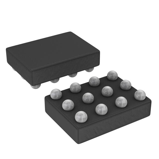
YZT PACKAGE(1)
(BOTTOM VIEW)
A B C D
1
2
3
(1)The
3
4
9
10
2
5
8
11
1
6
7
12
GND balls are internally connected.
1
A
IN1
B
NO1
C
COM1
D
NC1
2
VIO
GND
GND
V+
3
IN2
NO2
COM2
NC2
DESCRIPTION
The TS5A26542 is a dual single-pole double-throw (SPDT) analog switch that is designed to operate from 2.25 V
to 5.5 V. The device offers a low ON-state resistance with an excellent channel-to-channel ON-state resistance
matching, and the break-before-make feature to prevent signal distortion during the transferring of a signal from
one path to the another. The device has excellent total harmonic distortion (THD) performance and consumes
very low power. These features make this device suitable for portable audio applications.
The TS5A26542 has a separate logic supply pin (VIO) that operates from 1.65 V to 1.95 V. VIO powers the control
circuitry, which allows the TS5A26542 to be controlled by 1.8-V signals.
Table 1. ORDERING INFORMATION
TA
–40°C to 85°C
(1)
(2)
PACKAGE (1)
NanoFree™ – WCSP (DSBGA)
0.23-mm Large Bump – YZT
(Pb-free) 0.625-mm max height
ORDERABLE PART NUMBER
Reel of 3000
TS5A26542YZTR
TOP-SIDE MARKING (2)
_ _ _ JN_
For the most current package and ordering information, see the Package Option Addendum at the end of this document, or see the
TI website at www.ti.com.
YZT: The actual top-side marking has three preceding characters to denote year, month, and sequence code, and one following
character to designate the assembly/test site. Pin 1 identifier indicates solder-bump composition (1 = SnPb, • = Pb-free).
1
2
Please be aware that an important notice concerning availability, standard warranty, and use in critical applications of Texas
Instruments semiconductor products and disclaimers thereto appears at the end of this data sheet.
NanoFree is a trademark of Texas Instruments.
PRODUCTION DATA information is current as of publication date.
Products conform to specifications per the terms of the Texas
Instruments standard warranty. Production processing does not
necessarily include testing of all parameters.
Copyright © 2006–2009, Texas Instruments Incorporated
�TS5A26542
SCDS232E – JUNE 2006 – REVISED DECEMBER 2009
www.ti.com
SUMMARY OF CHARACTERISTICS (1)
2:1 Multiplexer/Demultiplexer
(2 × SPDT)
Configuration
Number of channels
2
ON-state resistance (ron)
0.75 Ω max
ON-state resistance match (Δron)
0.1 Ω max
ON-state resistance flatness (ron(flat))
0.1 Ω max
Turn-on/turn-off time (tON/tOFF)
25 ns/20 ns
Charge injection (QC)
15 pC
Bandwidth (BW)
43 MHz
OFF isolation (OISO)
–63 dB at 1 MHz
Crosstalk (XTALK)
–63 dB at 1 MHz
Total harmonic distortion (THD)
0.004%
Leakage current (INO(OFF)/INC(OFF))
20 nA
Package option
(1)
12-pin WCSP
V+ = 5 V, TA = 25°C
FUNCTION TABLE
NC TO COM,
COM TO NC
NO TO COM,
COM TO NO
L
ON
OFF
H
OFF
ON
IN
LOGIC DIAGRAM
IN1
(See Note A)
NC1
COM1
NO1
NC2
COM2
NO2
IN2
(See Note A)
A.
2
IN1 and IN2 are control inputs referenced to VIO.
Submit Documentation Feedback
Copyright © 2006–2009, Texas Instruments Incorporated
Product Folder Link(s): TS5A26542
�TS5A26542
www.ti.com
SCDS232E – JUNE 2006 – REVISED DECEMBER 2009
ABSOLUTE MAXIMUM RATINGS (1)
(2)
over operating free-air temperature range (unless otherwise noted)
V+
VIO
Supply voltage range
VNC
VNO
VCOM
Analog voltage range (3)
II/OK
Analog port diode current
INC
INO
ICOM
ON-state switch current
VI
Digital input voltage range (3)
IIK
Digital input clamp current
I+
IGND
Continuous current through V+ or GND
θJA
Package thermal impedance (7)
Tstg
Storage temperature range
(1)
(2)
(3)
(4)
(5)
(6)
(7)
(3)
(4) (5)
VNO, VNC, VCOM < 0 or VNO, VNC, VCOM > V+
ON-state peak switch current (6)
VNO, VNC, VCOM = 0 to V+
(4)
VI < 0
MIN
MAX
–0.5
6.5
V
–0.5
V+ + 0.5
V
–50
50
–450
450
–700
700
–0.5
6.5
UNIT
mA
mA
V
–50
–100
–65
mA
100
mA
102
°C/W
150
°C
Stresses beyond those listed under "absolute maximum ratings" may cause permanent damage to the device. These are stress ratings
only, and functional operation of the device at these or any other conditions beyond those indicated under "recommended operating
conditions" is not implied. Exposure to absolute-maximum-rated conditions for extended periods may affect device reliability.
The algebraic convention, whereby the most negative value is a minimum and the most positive value is a maximum
All voltages are with respect to ground, unless otherwise specified.
The input and output voltage ratings may be exceeded if the input and output clamp-current ratings are observed.
This value is limited to 5.5 V maximum.
Pulse at 1-ms duration
很抱歉,暂时无法提供与“TS5A26542YZTR”相匹配的价格&库存,您可以联系我们找货
免费人工找货