TUSB2551A
www.ti.com...................................................................................................................................................................................................... SCES790 – JUNE 2009
ADVANCED UNIVERSAL SERIAL BUS TRANSCEIVER
FEATURES
1
APPLICATIONS
•
•
•
Cellular Phones
Personal Digital Assistants (PDAs)
Handheld Computers
12
4
11
5
10
6
9
7
8
VCC(5.0)
VPU(3.3)
Vreg(3.3)
D+
D–
OE
SUSPEND
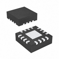
RGT PACKAGE
(BOTTOM VIEW)
VM
4
VP
3
RCV
2
SPEED
1
NC
•
3
SUSPEND
•
13
5
6
7
8
GND
(Exposed die pad)
16
15
14
13
VPU(3.3)
•
14
2
VCC(5.0)
•
SPEED
RCV
VP
VM
SOFTCON
GND
1
GND
•
VCC(I/O)
VCC(I/O)
•
PW PACKAGE
(TOP VIEW)
SOFTCON
•
Complies With Universal Serial Bus
Specification Rev. 2.0 (USB 2.0)
Transmits and Receives Serial Data at Both
Full-Speed (12-Mbit/s) and Low-Speed
(1.5-Mbit/s) Data Rates
Integrated Bypassable 5-V to 3.3-V Voltage
Regulator for Powering Via USB VBUS
Low-Power Operation is Ideal for Portable
Equipment
Meets the IEC-61000-4-2 Contact Discharge
(±9 kV) and Air-Gap Discharge (±9 kV) ESD
Ratings
Separate I/O Supply With Operation Down to
1.65 V
Very-Low Power Consumption to Meet USB
Suspend Current Requirements
No Power-Supply Sequencing Requirements
NC
•
9
OE
10
D–
11
D+
12
Vreg(3.3)
NC – No internal connection
DESCRIPTION/ORDERING INFORMATION
The TUSB2551A is a single-chip transceiver that complies with the physical-layer specifications of universal
serial bus (USB) 2.0. The device supports both full-speed (12-Mbit/s) and low-speed (1.5-Mbit/s) operation. The
TUSB2551A delivers superior edge-rate control, producing crisper eye diagrams, which ease the task of passing
USB compliance testing.
A dual supply-voltage operation allows the TUSB2551A to reference the system interface I/O signals to a supply
voltage down to 1.6 V, while independently powered by the USB VCC(5.0). This allows the system interface to
operate at its core voltage without the addition of buffering logic, and also reduce system operating current.
1
Please be aware that an important notice concerning availability, standard warranty, and use in critical applications of Texas
Instruments semiconductor products and disclaimers thereto appears at the end of this data sheet.
UNLESS OTHERWISE NOTED this document contains
PRODUCTION DATA information current as of publication date.
Products conform to specifications per the terms of Texas
Instruments standard warranty. Production processing does not
necessarily include testing of all parameters.
Copyright © 2009, Texas Instruments Incorporated
�TUSB2551A
SCES790 – JUNE 2009...................................................................................................................................................................................................... www.ti.com
ORDERING INFORMATION (1)
PACKAGE (2)
TA
QFN – RGT
–40°C to 85°C
(1)
(2)
TSSOP – PW
ORDERABLE PART NUMBER
Reel of 2000
TUSB2551ARGTR
Reel of 3000
TUSB2551APWR
Tube of 90
TUSB2551APW
TOP-SIDE MARKING
ZUH
PREVIEW
For the most current package and ordering information, see the Package Option Addendum at the end of this document, or see the TI
web site at www.ti.com.
Package drawings, thermal data, and symbolization are available at www.ti.com/packaging.
BLOCK DIAGRAM
To Internal
Circuitry
LDO
Regulator
VCC(I/O)
VCC(5.0)
Vreg(3.3)
VPU(3.3)
SOFTCON
D+
SPEED
OE
D–
Level
Translator
RCV
VP
VM
SUSPEND
GND
2
Submit Documentation Feedback
Copyright © 2009, Texas Instruments Incorporated
Product Folder Link(s): TUSB2551A
�TUSB2551A
www.ti.com...................................................................................................................................................................................................... SCES790 – JUNE 2009
TERMINAL FUNCTIONS
TERMINAL
NAME
NO.
I/O
DESCRIPTION
RGT
PW
VCC(I/O)
15
1
I
System interface supply voltage. Used to provide reference supply voltage for system I/O interface
signaling.
SPEED
1
2
I
Speed. Edge-rate control: A logic HIGH operates at edge rates for full-speed operation. A logic LOW
operates at edge rates for low-speed operation.
RCV
2
3
O
Receive data. Output for USB differential data.
VP
3
4
I/O
If OE = 1, VP = Receiver output (+)
If OE = 0, VP = Driver input (+)
VM
4
5
I/O
If OE = 1, VM = Receiver output (–)
If OE = 0, VM = Driver input (–)
SOFTCON
5
6
I
GND
6
7
SUSPEND
7
8
Soft connect. Controls state of VPU(3.3). See VPU(3.3) pin description for details.
Ground reference
I
Suspend. Active high. Turns off internal circuits to reduce supply current.
NC
8, 16
No internal connection
OE
9
9
I
D–, D+
10, 11
10, 11
I/O
Differential data lines conforming to the USB standard
Vreg(3.3)
12
12
O
3.3-V reference supply. Requires a minimum 0.1-µF decoupling capacitor for stability. A 1-µF capacitor is
recommended.
VPU(3.3)
13
13
O
Pullup supply voltage. Used to connect 1.5-kΩ pullup speed detect resistor.
If SOFTCON = 1, VPU(3.3) is high impedance. If SOFTCON = 0, VPU(3.3) = 3.3 V.
VCC(5.0)
14
14
I
USB bus supply voltage. Used to power USB transceiver and internal circuitry.
Output enable. Active low. Enables the transceiver to transmit data onto the bus. When inactive, the
transceiver is in the receive mode.
FUNCTIONAL DESCRIPTION
FUNCTION SELECTION
(1)
SUSPEND
OE
D+, D–
RCV
VP, VM
0
0
Driving
Active
Active
Normal transmit mode
FUNCTION
0
1
Receiving
Active
Active
Normal receive mode
1
0
Hi-Z
0
Not active
1
1
Hi-Z
0
Active
Low power state
Receiving during suspend (low power state) (1)
During suspend, VP and VM are active to detect out-of-band signaling conditions.
TRUTH TABLE DURING NORMAL MODE
OE = 0
INPUT
OUTPUT
RESULT
VP
VM
D+
D–
RCV
0
0
0
0
X (1)
SE0
0
1
0
1
0
Logic 0
1
0
1
0
1
Logic 1
1
1
1
1
X (1)
Undefined
OE = 1
INPUT
(1)
OUTPUT
RESULT
D+
D–
VP
VM
RCV
0
0
0
0
X (1)
SE0
0
1
0
1
0
Logic 0
1
0
1
0
1
Logic 1
1
1
1
1
X (1)
Undefined
X = Undefined
Submit Documentation Feedback
Copyright © 2009, Texas Instruments Incorporated
Product Folder Link(s): TUSB2551A
3
�TUSB2551A
SCES790 – JUNE 2009...................................................................................................................................................................................................... www.ti.com
Power-Supply Configurations
The TUSB2551A can be used with different power-supply configurations, which can be dynamically changed. An
overview is given in Table 1.
• Normal mode – Both VCC(I/O) and VCC(5.0) or VCC(5.0) and Vreg(3.3) are connected. For 5-V operation, VCC(5.0) is
connected to a 5-V source (4 V to 5.5 V). The internal voltage regulator then produces 3.3 V for the USB
connections. For 3.3-V operation, both VCC(5.0) and Vreg(3.3) are connected to a 3.3-V source (3 V to 3.6 V).
VCC(I/O) is independently connected to a voltage source (1.65 V to 3.6 V), depending on the supply voltage of
the external circuit.
• Disable mode – VCC(I/O) is not connected; VCC(5.0) or VCC(5.0) and Vreg(3.3) are connected. In this mode, the
internal circuits of the TUSB2551A ensure that the D+ and D– pins are in 3-state, and the power consumption
drops to the low-power (suspended) state level. Some hysteresis is built into the detection of VCC(I/O) lost.
• Sharing mode – VCC(I/O) is connected; VCC(5.0) and Vreg(3.3) are not connected. In this mode, the D+ and D–
pins are made 3-state, and the TUSB2551A allows external signals of up to 3.6 V to share the D+ and D–
lines. The internal circuits of the TUSB2551A ensure that virtually no current (maximum 10 mA) is drawn via
the D+ and D– lines. The power consumption through VCC(I/O) drops to the low-power (suspended) state level.
Both the VP and VM pins are driven HIGH to indicate this mode. Pin RCV is made LOW. Some hysteresis is
built into the detection of Vreg(3.3) lost.
Table 1. Power-Supply Configuration Overview
CONFIGURATION
MODE
VBUS/VTRM
VIF
Normal
Connected
Connected
Normal supply configuration and operation
Disconnect
(D+/D– sharing)
Open
Connected
VP/VM are HIGH outputs, RCV is LOW.
With OE = 0 and SUSPEND = 1, data lines may be driven
with external devices up to 3.6 V.
With D+, D– floating, ICC(I/O) draws less than 1 µA.
Disconnect
Ground
Connected
VP/VM are HIGH outputs, RCV is LOW.
With D+, D– floating, ICC(I/O)F draws less than 1 µA.
Disable Mode
Connected
Open
Prohibited
Connected
Ground
Notes
Logic controlled inputs pins are Hi-Z.
Prohibited condition
Table 2. Pin States in Disable or Sharing Mode
PINS
DISABLE-MODE STATE
SHARING-MODE STATE
VCC(5.0)/Vreg(3.3)
5-V input/3.3-V output, 3.3-V input/3.3-V input
Not present
VCC(I/O)
Not present
1.65-V to 3.6-V input
VPU(3.3)
High impedance (off)
High impedance (off)
D+, D–
High impedance
High impedance
VP, VM
Invalid (1)
H
RCV
Invalid (1)
L
Inputs (SPEED, SUSPEND, OE, SOFTCON)
High impedance
High impedance
(1)
4
High impedance or driven LOW
Submit Documentation Feedback
Copyright © 2009, Texas Instruments Incorporated
Product Folder Link(s): TUSB2551A
�TUSB2551A
www.ti.com...................................................................................................................................................................................................... SCES790 – JUNE 2009
Power-Supply Input Options
The TUSB2551A has two power-supply input options.
• Internal regulator – VCC(5.0) is connected to 4 V to 5.5 V. The internal regulator is used to supply the internal
circuitry with 3.3 V (nominal). Vreg(3.3) becomes a 3.3-V output reference.
• Regulator bypass – VCC(5.0) and Vreg(3.3) are connected to the same supply. The internal regulator is bypassed,
and the internal circuitry is supplied directly from the Vreg(3.3) power supply. The voltage range is
3 V to 3.6 V to comply with the USB specification.
The supply-voltage range for each input option is specified in Table 3.
Table 3. Power-Supply Input Options
INPUT OPTION
VCC(5.0)
Vreg(3.3)
VCC(I/O)
Internal regualtor
Supply input for internal regulator
(4 V to 5.5 V)
Voltage-reference output
(3.3 V, 300 µA)
Supply input for digital I/O pins
(1.4 V to 3.6 V)
Regulator bypass
Connected to Vreg(3.3) with
maximum voltage drop of 0.3 V
(2.7 V to 3.6 V)
Supply input
(3 V to 3.6 V)
Supply input for digital I/O pins
(1.4 V to 3.6 V)
Electrostatic Discharge (ESD)
PIN NAME
ESD
IEC61000-4-2, Air-Gap Discharge
D+, D–, VCC(5.0)
All other pins
IEC61000-4-2, Contact Discharge
TYP
±9
±9
Human-Body Model
±15
Human-Body Model
±2
Submit Documentation Feedback
Copyright © 2009, Texas Instruments Incorporated
Product Folder Link(s): TUSB2551A
UNIT
kV
kV
5
�TUSB2551A
SCES790 – JUNE 2009...................................................................................................................................................................................................... www.ti.com
ABSOLUTE MAXIMUM RATINGS (1)
over operating free-air temperature range (unless otherwise noted)
MIN
MAX
VCC(5.0)
Supply voltage range
–0.5
6
V
VCC(I/O)
I/O supply voltage range
–0.5
4.6
V
Vreg(3.3)
Regulated voltage range
–0.5
4.6
VI
DC input voltage range
–0.5
VCC(I/O) + 0.5
mA
IO(D+, D-)
Output current (D+, D–)
±50
mA
IO
Output current (all others)
±15
mA
II
Input Current
±50
mA
Tstg
Storage temperature range
150
°C
(1)
–65
UNIT
V
Stresses beyond those listed under "absolute maximum ratings" may cause permanent damage to the device. These are stress ratings
only, and functional operation of the device at these or any other conditions beyond those indicated under "recommended operating
conditions" is not implied. Exposure to absolute-maximum-rated conditions for extended periods may affect device reliability.
RECOMMENDED OPERATING CONDITIONS
MIN
NOM
MAX
UNIT
VCC(5.0)
Supply voltage, internal regulator option
5-V operation
4
5
5.25
V
Vreg(3.3)
Supply voltage, regulator bypass option
3.3-V operation
3
3.3
3.6
V
VCC(I/O)
I/O supply voltage
3.6
V
1.65
VIL
Low-level input voltage
(1)
VCC(I/O) –0.3
0.15 VCC(I/O)
V
VIH
High-level input voltage (1)
0.85 VCC(I/O)
VCC(I/O) + 0.3
V
D+, D–
Input voltage on analog I/O pins
0
3.6
V
Tc
Junction temperature
–40
85
°C
(1)
6
Specification applies to the following pins: SUSPEND, SPEED, RCV, SOFTCON, VP, VM, and OE.
Submit Documentation Feedback
Copyright © 2009, Texas Instruments Incorporated
Product Folder Link(s): TUSB2551A
�TUSB2551A
www.ti.com...................................................................................................................................................................................................... SCES790 – JUNE 2009
DC ELECTRICAL CHARACTERISTICS – SYSTEM AND USB INTERFACE (1)
VCC(I/O) = 3.6 V, VCC(5.0) = 5 V (unless otherwise noted), TA = 25°C. Bold indicates specifications over temperature, –40°C to
85°C.
PARAMETER
VOH
High-level output
voltage (2)
VOL
Low-level output
voltage (2)
IIL
Input leakage current
ICC(I/O)
ICC(5.0)
TEST CONDITIONS
MIN
IOH = 20 µA
TYP
MAX
0.9 VCC(I/O)
V
IOL = 20 µA
(2)
–5
0.1
V
1.5
5
µA
SPEED
SUSPEND
OE
1
0
1
1
5
1
0
0
1
5
0
0
1
1
5
0
0
0
1
5
0
1
0
VCC(I/O) supply current
VCC(5.0) supply current
VOLTAGE
UNIT
LOAD
VCC(5.0) =
5.25 V,
VCC(I/O) =
3.6 V
1
5
1
2
mA
260
280
µA
1
0
0
f = 6 MHz,
CL = 50 pF
0
0
0
f = 750 kHz,
CL = 600 pF
1
0
1
800
1100
1
0
0
3000
5000
0
0
1
230
350
0
0
0
400
700
0
1
0
130
200
1
0
0
f = 6 MHz,
CL = 50 pF
6
10
0
0
0
f = 750 kHz,
CL = 600 pF
4..3
5
VCC(5.0) =
5.25 V,
VCC(I/O) =
3.6 V
µA
µA
mA
IPU(3.3)LEAK
VPU(3.3) leakage current SOFTCON = 1, VPU(3.3) = 0 V
–5
5
µA
ICC(I/O)LEAK
VCC(I/O) leakage current VCC(I/O) = 3.6 V, VCC(5.0) = 0 V
–5
5
µA
VPU(3.3)
Pullup output voltage
Ireg(3.3) = 200 µA, VCC(5.0) = 4 V to 5.25 V
3.6
V
RSW
VPU(3.3) switch
resistance
Ireg(3.3) = 10 mA, VCC(5.0) = 4 V to 5.25 V
10
10 pulses
±9
10 pulses
±9
3
3.3
Ω
ESD Protection
IEC-61000-4-2 Air-Gap Discharge
(D+, D–,
Contact Discharge
VCC(5.0) only)
(1)
(2)
kV
Specification for packaged product only
Specification applies to the following pins: RCV, VP, VM, OE.
Submit Documentation Feedback
Copyright © 2009, Texas Instruments Incorporated
Product Folder Link(s): TUSB2551A
7
�TUSB2551A
SCES790 – JUNE 2009...................................................................................................................................................................................................... www.ti.com
DC ELECTRICAL CHARACTERISTICS – TRANSCEIVER (1)
PARAMETER
TEST CONDITIONS
MIN
TYP
MAX
UNIT
Leakage Current
ILO
Hi-Z state data line leakage (suspend mode)
0 V < VIN < 3.3 V, SUSPEND = 1
–10
10
µA
Input Levels
VDI
Differential input sensitivity
|(D+) – (D–)|
0.2
VCM
Differential common mode range
Includes VDI range
0.8
2.5
V
VSE
Single-ended receiver threshold
0.8
2
V
Receiver hysteresis
V
200
mV
Output Levels
VOL
Static output low
RL = 1.5 kΩ to 3.6 V
VOH
Static output high
RL = 15 kΩ to GND
2.8
0.3
V
3.6
V
Capacitance
CIN
Transceiver capacitance
Pin to GND
ZDRV
Driver output resistance
Steady-state drive
(1)
8
10
1
6
pF
11
Ω
Specification for packaged product only
Submit Documentation Feedback
Copyright © 2009, Texas Instruments Incorporated
Product Folder Link(s): TUSB2551A
�TUSB2551A
www.ti.com...................................................................................................................................................................................................... SCES790 – JUNE 2009
AC ELECTRICAL CHARACTERISTICS (1)
PARAMETER
TEST CONDITIONS
MIN
MAX
UNIT
Driver Characteristics (Low Speed)
TR
Transition rise time
CL = 200 pF (see Figure 2), CL = 600 pF
75
300
ns
TF
Transition fall time
CL = 200 pF (see Figure 2), CL = 600 pF
75
300
ns
LRFM
Rise/fall time matching
TR, TF
VCRS
Output signal crossover voltage
80
125
%
1.3
2
V
Driver Characteristics (Full Speed)
TR
Transition rise time
CL = 50 pF (see Figure 2)
4
20
ns
TF
Transition fall time
CL = 50 pF (see Figure 2)
4
20
ns
FRFM
Rise/fall time matching
TR, TF
90
111.1
%
VCRS
Output signal crossover voltage
1.3
2
V
15
ns
Transceiver Timing (Full Speed)
tPVZ
OE to receiver 3-state delay
See Figure 1
tPZD
Receiver 3-state to transmit delay
See Figure 1
tPDZ
OE to driver 3-state delay
See Figure 1
tPZV
Driver 3-state to receive delay
See Figure 1
tPLH
tPHL
VP, VM to D+, D– propagation delay
See Figure 4
17
ns
tPLH
tPHL
D+, D– to RCV propagation delay
See Figure 3
17
ns
tPLH
tPHL
D+, D– to VP, VM propagation delay
See Figure 3
10
ns
(1)
15
ns
15
15
ns
ns
Specification for packaged product only
Submit Documentation Feedback
Copyright © 2009, Texas Instruments Incorporated
Product Folder Link(s): TUSB2551A
9
�TUSB2551A
SCES790 – JUNE 2009...................................................................................................................................................................................................... www.ti.com
TIMING DIAGRAMS
RECEIVE
TRANSMIT
OE
tPVZ
t PZV
VP/VM
tPZD
tPDZ
D+/D–
Figure 1. Enable and Disable Times
FALL TIME
RISE TIME
Differential
Data Lines
90%
90%
10%
10%
tR
tF
Figure 2. Rise and Fall Times
D+
VCRS
D–
Differential
Data Lines
VCRS
tPHL
tPLH
VOH
VOL
VSS
Figure 3. Receiver Propagation Delay
VOH
VOL
D+
tPLH
tPHL
VCRS
D–
Differential
Data Lines
VCRS
Figure 4. Driver Propagation Delay
10
Submit Documentation Feedback
Copyright © 2009, Texas Instruments Incorporated
Product Folder Link(s): TUSB2551A
�TUSB2551A
www.ti.com...................................................................................................................................................................................................... SCES790 – JUNE 2009
TEST CIRCUITS
D.U.T.
25 pF
Figure 5. Load for VP, VM, RCV
VTRM
15k
D. U. T.
20
15k
CL
Figure 6. Load for D+, D–
Submit Documentation Feedback
Copyright © 2009, Texas Instruments Incorporated
Product Folder Link(s): TUSB2551A
11
�PACKAGE OPTION ADDENDUM
www.ti.com
10-Dec-2020
PACKAGING INFORMATION
Orderable Device
Status
(1)
Package Type Package Pins Package
Drawing
Qty
Eco Plan
(2)
Lead finish/
Ball material
MSL Peak Temp
Op Temp (°C)
Device Marking
(3)
(4/5)
(6)
TUSB2551ARGTR
ACTIVE
VQFN
RGT
16
3000
RoHS & Green
NIPDAU
Level-1-260C-UNLIM
-40 to 85
ZUH
(1)
The marketing status values are defined as follows:
ACTIVE: Product device recommended for new designs.
LIFEBUY: TI has announced that the device will be discontinued, and a lifetime-buy period is in effect.
NRND: Not recommended for new designs. Device is in production to support existing customers, but TI does not recommend using this part in a new design.
PREVIEW: Device has been announced but is not in production. Samples may or may not be available.
OBSOLETE: TI has discontinued the production of the device.
(2)
RoHS: TI defines "RoHS" to mean semiconductor products that are compliant with the current EU RoHS requirements for all 10 RoHS substances, including the requirement that RoHS substance
do not exceed 0.1% by weight in homogeneous materials. Where designed to be soldered at high temperatures, "RoHS" products are suitable for use in specified lead-free processes. TI may
reference these types of products as "Pb-Free".
RoHS Exempt: TI defines "RoHS Exempt" to mean products that contain lead but are compliant with EU RoHS pursuant to a specific EU RoHS exemption.
Green: TI defines "Green" to mean the content of Chlorine (Cl) and Bromine (Br) based flame retardants meet JS709B low halogen requirements of


 工商网监
湘ICP备2023018690号
工商网监
湘ICP备2023018690号
