NPN SILICON GERMANIUM RF TRANSISTOR
NESG260234
NPN SiGe RF TRANSISTOR FOR
MEDIUM OUTPUT POWER AMPLIFICATION (1 W)
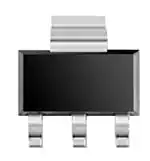
3-PIN POWER MINIMOLD (34 PKG)
FEATURES
• This product is suitable for medium output power (1 W) amplification
Pout = 30 dBm TYP. @ VCE = 6 V, Pin = 15 dBm, f = 460 MHz
Pout = 30 dBm TYP. @ VCE = 6 V, Pin = 20 dBm, f = 900 MHz
• MSG (Maximum Stable Gain) = 23 dB TYP. @ VCE = 6 V, Ic = 100 mA, f = 460 MHz
• Using UHS2-HV process (SiGe technology), VCBO (ABSOLUTE MAXIMUM RATINGS) = 25 V
• 3-pin power minimold (34 PKG)
ORDERING INFORMATION
Part Number
NESG260234
Order Number
Package
NESG260234-AZ
3-pin power minimold
(Pb-Free)
NESG260234-T1
Quantity
Note1, 2
25 pcs
Supplying Form
• Magazine case
(Non reel)
NESG260234-T1-AZ
1 kpcs/reel
• 12 mm wide embossed taping
• Pin 2 (Emitter) face the perforation side of the tape
Notes 1. Contains Lead in the part except the electrode terminals.
2. With regards to terminal solder (the solder contains lead) plated products (conventionally plated),
contact
your nearby sales office.
Remark To order evaluation samples, contact your nearby sales office.
Unit sample quantity is 25 pcs.
ABSOLUTE MAXIMUM RATINGS (T A = +25C)
Parameter
Symbol
Ratings
Unit
Collector to Base Voltage
VCBO
25
V
Collector to Emitter Voltage
VCEO
9.2
V
Emitter to Base Voltage
VEBO
2.8
V
IC
600
mA
1.9
W
Collector Current
Total Power Dissipation
Ptot
Note
Junction Temperature
Tj
150
C
Storage Temperature
Tstg
65 to +150
C
2
Note Mounted on 34.2 cm 0.8 mm (t) glass epoxy PWB
Caution: Observe precautions when handling because these devices are sensitive to electrostatic discharge
Document No. PU10547EJ02V0DS (2nd edition)
Date Published May 2005 CP(K)
The mark shows major revised points.
�NESG260234
THERMAL RESISTANCE (T A = +25C)
Parameter
Termal Resistance from Junction to
Ambient
Symbol
Ratings
Unit
Rthj-a
65
C/W
Note
2
Note Mounted on 34.2 cm 0.8 mm (t) glass epoxy PWB
RECOMMENDED OPERATING RANGE (T A = +25C)
Parameter
Collector to Emitter Voltage
Collector Current
Input Power
Note
Symbol
MIN.
TYP.
MAX.
Unit
VCE
6.0
7.2
V
IC
400
500
mA
Pin
15
20
dBm
Note Input power under conditions of VCE 6.0 V, f = 460 MHz
2
Data Sheet PU10547EJ02V0DS
�NESG260234
ELECTRICAL CHARACTERISTICS (T A = +25C)
Parameter
Symbol
Test Conditions
MIN.
TYP.
MAX.
Unit
DC Characteristics
Collector Cut-off Current
ICBO
VCB = 9.2 V, IE = 0 mA
1
A
Emitter Cut-off Current
IEBO
VEB = 1.0 V, IC = 0 mA
1
A
VCE = 3 V, IC = 100 mA
80
120
180
VCE = 6 V, IC (set) = 30 mA (RF OFF),
19
22
dB
19
dB
28.5
30.0
dBm
30.0
dBm
50
%
60
%
DC Current Gain
hFE
Note
RF Characteristics
Linner Gain (1)
GL
f = 460 MHz, Pin = 0 dBm
Linner Gain (2)
GL
VCE = 6 V, IC (set) = 30 mA (RF OFF),
f = 900 MHz, Pin = 0 dBm
Output Power (1)
Pout
VCE = 6 V, IC (set) = 30 mA (RF OFF),
f = 460 MHz, Pin = 15 dBm
Output Power (2)
Pout
VCE = 6 V, IC (set) = 30 mA (RF OFF),
f = 900 MHz, Pin = 20 dBm
C
Collector Efficiency (1)
VCE = 6 V, IC (set) = 30 mA (RF OFF),
f = 460 MHz, Pin = 15 dBm
C
Collector Efficiency (2)
VCE = 6 V, IC (set) = 30 mA (RF OFF),
f = 900 MHz, Pin = 20 dBm
Note Pulse measurement: PW 350 s, Duty Cycle 2%
hFE CLASSIFICATION
Rank
FB
Marking
SP
hFE Value
80 to 180
Data Sheet PU10547EJ02V0DS
3
�NESG260234
TYPICAL CHARACTERISTICS (T A = +25C, unless otherwise specified)
Remark The graphs indicate nominal characteristics.
4
Data Sheet PU10547EJ02V0DS
�NESG260234
Remark The graphs indicate nominal characteristics.
Data Sheet PU10547EJ02V0DS
5
�NESG260234
Remark The graphs indicate nominal characteristics.
6
Data Sheet PU10547EJ02V0DS
�NESG260234
S-PARAMETERS
PA EVALUATION CIRCUIT TYPICAL CHARACTERISTICS
Remark The graphs indicate nominal characteristics.
Data Sheet PU10547EJ02V0DS
7
�NESG260234
EVALUATION CIRCUIT (f = 460 MHz)
The application circuits and their parameters are for reference only and are not intended for use in actual design-ins.
EVALUATION BOARD (f = 460 MHz)
Notes
1. 20 20 mm, t = 0.8 mm double sided copper clad glass epoxy PWB.
2. Back side: GND pattern
3. Solder gold plated on pattern
4.
8
: Through holes
Data Sheet PU10547EJ02V0DS
�NESG260234
COMPONENT LIST
Component
Maker
Value
Size (TYPE)
Purpose
C1
Murata
10 pF
1005
Input DC Block/Input RF Matching
C2
Murata
4 pF
1005
Input RF Matching
C3
Murata
33 pF
1005
Input DC Block/Output RF Matching
C4
Murata
10 000 pF
1005
RF GND
C5
Murata
1 F
1608
RF GND
L1
Toko
68 nH
1005
RF Block/Input RF Matching
L2
Toko
33 nH
LLQ2021
L3
Toko
1 nH
1005
Input RF Matching
L4
Toko
8.2 nH
1005
Input RF Matching
L5
Toko
8.2 nH
LLQ2021
R1
SSM
15
1608
RF Block/Output RF Matching
Output RF Matching
Improve Stability
Data Sheet PU10547EJ02V0DS
9
�NESG260234
PACKAGE DIMENSIONS
3-PIN POWER MINIMOLD (34 PKG) (UNIT: mm)
10
Data Sheet PU10547EJ02V0DS
�
很抱歉,暂时无法提供与“NESG260234-T1-AZ”相匹配的价格&库存,您可以联系我们找货
免费人工找货