CY29775
2.5V or 3.3V, 200-MHz, 14 Output Zero Delay Buffer
Features
■ ■ ■ ■ ■ ■ ■ ■ ■ ■ ■ ■ ■
Description
The CY29775 is a low-voltage high-performance 200-MHz PLL-based zero delay buffer designed for high-speed clock distribution applications. The CY29775 features two reference clock inputs and provides 14 outputs partitioned in 3 banks of 5, 5, and 4 outputs. Bank A and Bank B divide the VCO output by 4 or 8 while Bank C divides by 8 or 12 per SEL(A:C) settings, see Function Table (Bank A, B, and C) on page 4. These dividers allow output to input ratios of 6:1, 4:1, 3:1, 2:1, 3:2, 4:3, 1:1, and 2:3. Each LVCMOS compatible output can drive 50Ω series or parallel terminated transmission lines. For series terminated transmission lines, each output can drive one or two traces giving the device an effective fanout of 1:28. The PLL is ensured stable given that the VCO is configured to run between 200 MHz to 500 MHz. This allows a wide range of output frequencies from 8.3 MHz to 200 MHz. For normal operation, the external feedback input, FB_IN, is connected to the feedback output, FB_OUT. The internal VCO is running at multiples of the input reference clock set by the feedback divider, see Frequency Table on page 4. When PLL_EN is LOW, PLL is bypassed and the reference clock directly feeds the output dividers. This mode is fully static and the minimum input clock frequency specification does not apply.
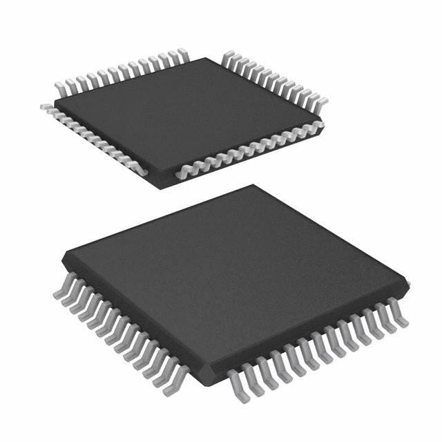
Output frequency range: 8.3 MHz to 200 MHz Input frequency range: 4.2 MHz to 125 MHz 2.5V or 3.3V operation Split 2.5V/3.3V outputs 14 Clock outputs: Drive up to 28 clock lines 1 Feedback clock output 2 LVCMOS reference clock inputs 150 ps max output-output skew PLL bypass mode Spread Aware™ Output enable/disable Industrial temperature range: –40°C to +85°C 52-Pin 1.0-mm TQFP package
Block Diagram
V C O _S E L(1,0) P LL_E N TCLK_SEL T C LK 0 TC LK1 F B _IN PLL 200 5 0 0M H z
÷2 ÷4 ÷2 / ÷4 C LK STOP
S E LA
÷2 / ÷4 C LK STOP
Q A0 Q A1 Q A2 Q A3 Q A4 QB0 QB1 Q B2 Q B3 QB4 QC0 QC1 QC2 QC3
S E LB
÷4 / ÷6
C LK STOP
SELC C LK _S T P #
÷ 4 / ÷ 6 / ÷ 8 / ÷ 12
F B _O U T
F B _S E L(1,0) M R #/O E
Cypress Semiconductor Corporation Document #: 38-07480 Rev. *A
•
198 Champion Court
•
San Jose, CA 95134-1709 • 408-943-2600 Revised December 19, 2007
[+] Feedback
�CY29775
Pinouts
Figure 1. Pin Diagram - 52-Pin 1.0-mm TQFP package
VCO_SEL0 QC1 VDDQC VSS QC3 VDDQC VDDQB NC
52 51 50 49 48 47 46 45 44 43 42 41 40 V SS MR#/OE CLK_STP# SELB SELC PLL_EN SELA TCLK_SEL TCLK0 TCLK1 V CO_SEL1 V DD A V DD 1 2 3 4 5 6 7 8 9 10 11 12 13 39 38 37 36 35 34 33 32 31 30 29 28 27 V SS QB1 V DDQB QB2 V SS QB3 V DDQB QB4 FB_IN V SS FB_OUT V DDFB NC
14 15 16 17 18 19 20 21 22 23 24 25 26 FB_SEL0 QA4 AVSS QA3 VDDQA FB_SEL1 VSS QA1 VDDQA QA2 QA0 VSS VDDQA
Table 1. Pin Definition - 52-Pin 1.0-mm TQFP package Pin[1] 9 10 16, 18, 21, 23, 25 32, 34, 36, 38, 40 44, 46, 48, 50 29 31 Name TCLK0 TCLK1 QA(4:0) QB(4:0) QC(3:0) FB_OUT FB_IN IO I, PD I, PU O O O O I, PU Type LVCMOS LVCMOS LVCMOS LVCMOS LVCMOS LVCMOS LVCMOS Description LVCMOS/LVTTL reference clock input LVCMOS/LVTTL reference clock input Clock output bank A Clock output bank B Clock output bank C Feedback clock output. Connect to FB_IN for normal operation. Feedback clock input. Connect to FB_OUT for normal operation. This input must be at the same voltage rail as input reference clock. See Table 2 on page 4. Output enable/disable input. See Table 3 on page 4. Clock stop enable/disable input. See Table 3 on page 4. PLL enable/disable input. See Table 3 on page 4. Reference select input. See Table 3 on page 4. VCO divider select input. See Tables 3, 4 and 5. Frequency select input, Bank (A:C). See Table 4 on page 4. Feedback dividers select inputs. See Table 5 on page 5. 2.5V or 3.3V Power supply for bank A output clocks[2,3] 2.5V or 3.3V Power supply for bank B output clocks[2,3]
QC0 VSS
CY29775
QC2 VSS
QB0
2 3 6 8 11, 52 7, 4, 5 20, 14 17, 22, 26 33, 37, 41
MR#/OE CLK_STP# PLL_EN TCLK_SEL VCO_SEL(1,0) SEL(A:C) FB_SEL(1,0) VDDQA VDDQB
I, PU I, PU I, PU I, PD I, PD I, PD I, PD Supply Supply
LVCMOS LVCMOS LVCMOS LVCMOS LVCMOS LVCMOS LVCMOS VDD VDD
Notes 1. PU = Internal pull up, PD = Internal pull down 2. A 0.1-μF bypass capacitor must be placed as close as possible to each positive power pin (


 工商网监
湘ICP备2023018690号
工商网监
湘ICP备2023018690号
