CY7B9234
CY7B9334
SMPTE HOTLink® Transmitter/Receiver
Features
■
SMPTE-259M-CD compliant along with SMPTE-259M
encoder (CY7C9235) and decoder (CY7C9335)
■
Fibre Channel compliant
■
DVB-ASI compliant
■
RX PLL tolerant of long run length data patterns (>20 bits)
■
8B/10B-coded or 10-bit unencoded
■
TTL synchronous I/O
■
No external PLL components
■
Triple PECL 100K serial outputs
■
Dual PECL 100K serial inputs
■
Low power: 350 mW (Tx), 650 mW (Rx)
■
Compatible with fiber-optic modules, coaxial cable, and twisted
pair media
■
Built-In Self-Test
■
Single +5V supply
■
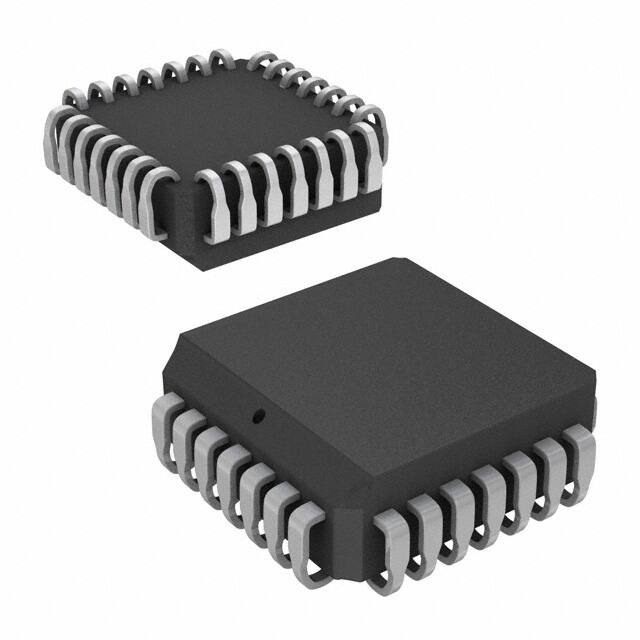
28-pin PLCC
■
0.8μ BiCMOS
transfer uncompressed SMPTE-259M encoded video over
high-speed serial links (fiber, coax, and twisted pair). SMPTE
HOTLink supports SMPTE-259M-CD standard data rates at 270
and 360 Mbps. Figure 1 illustrates typical connections to host
systems or controllers.
Eight or ten bits of user data or protocol information are loaded
into the SMPTE HOTLink transmitter and, in DVB mode, are
encoded. Serial data is shifted out of the three differential
positive ECL (PECL) serial ports at the bit rate (which is 10 times
the byte rate).
The SMPTE HOTLink receiver accepts the serial bit stream at its
differential line receiver inputs and, using a completely integrated
PLL Clock Synchronizer, recovers the timing information
necessary for data reconstruction. The bit stream is deserialized,
and in DVB mode, decoded and checked for transmission errors.
Recovered bytes are presented in parallel to the receiving host
along with a byte rate clock.
The 8B/10B encoder/decoder can be disabled in SMPTE or DVB
systems that already encode or scramble the transmitted data.
I/O signals are available to create a seamless interface with both
asynchronous FIFOs (i.e., CY7C42X) and clocked FIFOs (i.e.,
CY7C44X). A Built-In Self-Test pattern generator and checker
allows testing of the transmitter, receiver, and the connecting link
as a part of a system diagnostic check.
SMPTE HOTLink devices are ideal for a variety of video applications including video transmission equipment, video recorders,
video editing equipment, and video routers.
Functional Description
The CY7B9234 SMPTE HOTLink® Transmitter and CY7B9334
SMPTE HOTLink Receiver bolt on to the SMPTE Scrambler
Controller (CY7C9235) and SMPTE Descrambler/Framer
Controller (CY7C9335) completing the four piece chipset to
CY7B9234 Transmitter Logic Block Diagram
CY7B9334 Receiver Logic Block Diagram
SC/D (Da)
RP ENN
ENA
D0− 7
(Db − h)
RF
SVS(Dj)
FOTO
ENABLE
INPUT REGISTER
CKW
INA+
INA−
PECL
TTL
SO
OUTA
SHIFTER
OUTB
TEST
LOGIC
SHIFTER
DECODER
REGISTER
CLOCK
SYNC
DECODER
REFCLK
OUTC
MODE
BISTEN
DATA
INB (INB+)
SI(INB− )
ENCODER
CLOCK
GENERATOR
FRAMER
A/B
MODE
OUTPUT
REGISTER
TEST
LOGIC
BISTEN
CKR
RDY
Q0− 7
(Qb − h)
RVS(Qj)
SC/D (Qa)
Cypress Semiconductor Corporation
Document #: 38-02014 Rev. *B
•
198 Champion Court
•
San Jose, CA 95134-1709
•
408-943-2600
Revised December 15, 2009
[+] Feedback
�CY7B9234
CY7B9334
Contents
Features ............................................................................... 1
Functional Description ....................................................... 1
CY7B9234 Transmitter Pin Configuration ........................ 3
CY7B9334 Receiver Pin Configuration ............................. 3
Pin Description ................................................................... 3
CY7B9234 SMPTE HOTLink Transmitter ..................... 3
Pin Description ................................................................... 5
CY7B9334 SMPTE HOTLink Receiver ......................... 5
CY7B9234 SMPTE HOTLink Transmitter Block Diagram Description .............................................................................. 6
Input Register ................................................................ 6
Encoder ......................................................................... 6
Shifter ............................................................................ 6
OutA, OutB, OutC .......................................................... 6
Clock Generator ............................................................ 6
Test Logic ...................................................................... 7
CY7B9334 SMPTE HOTLink Receiver
Block Diagram Description ................................................ 7
Serial Data Inputs .......................................................... 7
PECL-TTL Translator .................................................... 7
Clock Synchronization ................................................... 7
Framer ........................................................................... 7
Shifter ............................................................................ 7
Decode Register ............................................................ 7
Decoder ......................................................................... 7
Output Register ............................................................. 8
Test Logic ...................................................................... 8
Maximum Ratings ............................................................... 9
Operating Range ................................................................. 9
CY7B9234/CY7B9334 Electrical Characteristics Over the
Operating Range.................................................................. 9
Capacitance ....................................................................... 10
AC Test Loads and Waveforms ....................................... 10
Transmitter Switching Characteristics Over the Operating
Range.................................................................................. 10
Receiver Switching Characteristics Over the
Operating Range................................................................ 11
Switching Waveforms for the CY7B9234 SMPTE HOTLink
Transmitter ........................................................................ 12
Switching Waveforms for the CY7B9334
Document #: 38-02014 Rev. *B
SMPTE HOTLink Receiver ................................................13
SMPTE HOTLink CY7B9234 Transmitter and CY7B9334 Receiver Operation ................................................................14
CY7B9234 SMPTE HOTLink Transmitter
Operating Mode Description ............................................16
Encoded Mode Operation ............................................16
Bypass Mode Operation ...............................................16
PECL Output Functional and Connection
Options ................................................................................17
Transmitter Serial Data Characteristics ..........................18
Transmitter Test Mode Description .................................18
BIST Mode ...................................................................19
Test Mode ....................................................................20
CY7B9334 SMPTE HOTLink Receiver
Operating Mode Description ............................................20
Encoded Mode Operation ............................................20
Bypass Mode Operation ...............................................20
Parallel Output Function ...............................................21
Receiver Serial Data Requirements .................................21
Receiver Test Mode Description ......................................21
BIST Mode ...................................................................22
Test Mode ....................................................................22
8B/10B Codes and Notation Conventions .......................22
Notation Conventions ...................................................22
8B/10B Transmission Code ..........................................23
Transmission Order ......................................................23
Valid and Invalid Transmission Characters ..................23
Use of the Tables for Generating
Transmission Characters .....................................................24
Use of the Tables for Checking the Validity
of Received Transmission Characters .................................24
Valid Data Characters (SC/D = LOW) ...............................24
Valid Special Character Codes and Sequences (SC/D =
HIGH) ...................................................................................33
Ordering Information .........................................................34
Package Diagram ...............................................................35
Document History Page ....................................................36
Sales, Solutions, and Legal Information .........................36
Page 2 of 36
[+] Feedback
�CY7B9234
CY7B9334
PROTOCOL
LOGIC
RECEIVE
MESSAGE
BUFFER
SMPTE Serializer
CY7B9234
SMPTE Encoder
CY7C9235
7B9234
TRANSMIT
MESSAGE
BUFFER
SMPTE Decoder
CY7C9335
SERIAL LINK
SMPTE Deserializer
CY7B9334
PROTOCOL
LOGIC
Figure 1. SMPTE HOTLink System Connections
HOST
HOST
CY7B9234 Transmitter Pin Configuration
CY7B9334 Receiver Pin Configuration
PLCC
Top View
VCCN
OUTC+
OUTC−
OUTB−
OUTB+
OUTA+
OUTA−
BISTEN
A/B
INA+
INA−
INB (INB+)
SI (INB−)
MODE
PLCC
Top View
4 3 2 1 28 2726
25
24
23
22
21
20
19
FOTO
ENN
ENA
VCCQ
CKW
GND
SC/D(D a)
4 3 2 1 28 2726
RF
GND
RDY
GND
VCCN
RVS (Qj)
(Qh) Q7
5
6
7
7B9334
8
9
10
11 1213 14 15 16 1718
25
24
23
22
21
20
19
REFCLK
VCCQ
SO
CKR
VCCQ
GND
SC/D (Qa)
(Qg ) Q 6
(Q f ) Q 5
(Q i ) Q 4
(Qe ) Q 3
(Qd ) Q 2
(Q c ) Q 1
(Qb ) Q 0
5
6
7
7B9234
8
9
10
11 1213 14 15 16 1718
(Dg ) D6
(D f ) D5
(D i ) D4
(De ) D3
(Dd ) D2
(D c ) D1
(Db ) D0
BISTEN
GND
MODE
RP
VCCQ
SVS(D j)
(Dh)D 7
Pin Description
CY7B9234 SMPTE HOTLink Transmitter
Name
I/O
Description
D0−7
(Db − h)
TTL In
Parallel Data Input. Data is clocked into the Transmitter on the rising edge of CKW if ENA is LOW
(or on the next rising CKW with ENN LOW). If ENA and ENN are HIGH, a Null character (K28.5) is
sent. When MODE is HIGH, D0, 1, ...7 become Db, c,...h respectively.
SC/D (Da)
TTL In
Special Character/Data Select. A HIGH on SC/D when CKW rises causes the transmitter to encode
the pattern on D0−7 as a control code (Special Character), while a LOW causes the data to be coded
using the 8B/10B data alphabet. When MODE is HIGH, SC/D (Da) acts as Da input. SC/D has the
same timing as D0−7.
SVS
(Dj)
TTL In
Send Violation Symbol. If SVS is HIGH when CKW rises, a Violation symbol is encoded and sent
while the data on the parallel inputs is ignored. If SVS is LOW, the state of D0−7 and SC/D determines
the code sent. In normal or test mode, this pin overrides the BIST generator and forces the transmission of a Violation code. When MODE is HIGH (placing the transmitter in unencoded mode), SVS
(Dj) acts as the Dj input. SVS has the same timing as D0−7.
ENA
TTL In
Enable Parallel Data. If ENA is LOW on the rising edge of CKW, the data is loaded, encoded, and
sent. If ENA and ENN are HIGH, the data inputs are ignored and the Transmitter will insert a Null
character (K28.5) to fill the space between user data. ENA may be held HIGH/LOW continuously or
it may be pulsed with each data byte to be sent. If ENA is being used for data control, ENN will normally
be strapped HIGH, but can be used for BIST function control.
Document #: 38-02014 Rev. *B
Page 3 of 36
[+] Feedback
�CY7B9234
CY7B9334
Pin Description
CY7B9234 SMPTE HOTLink Transmitter (continued)
Name
I/O
Description
ENN
TTL In
Enable Next Parallel Data. If ENN is LOW, the data appearing on D0−7 at the next rising edge of
CKW is loaded, encoded, and sent. If ENA and ENN are HIGH, the data appearing on D0−7 at the
next rising edge of CKW will be ignored and the Transmitter will insert a Null character to fill the space
between user data. ENN may be held HIGH/LOW continuously or it may be pulsed with each data
byte sent. If ENN is being used for data control, ENA will normally be strapped HIGH, but can be used
for BIST function control.
CKW
TTL In
Clock Write. CKW is both the clock frequency reference for the multiplying PLL that generates the
high-speed transmit clock, and the byte rate write signal that synchronizes the parallel data input.
CKW must be connected to a crystal controlled time base that runs within the specified frequency
range of the Transmitter and Receiver.
FOTO
TTL In
Fiber-Optic Transmitter Off. FOTO determines the function of two of the three PECL transmitter
output pairs. If FOTO is LOW, the data encoded by the Transmitter will appear at the outputs continuously. If FOTO is HIGH, OUTA± and OUTB± are forced to their “logic zero” state (OUT+ = LOW and
OUT− = HIGH), causing a fiber-optic transmit module to extinguish its light output. OUTC is unaffected
by the level on FOTO, and can be used as a loop-back signal source for board-level diagnostic testing.
OUT A±
OUT B±
OUT C±
PECL Out
Differential Serial Data Outputs. These PECL 100K outputs (+5V referenced) are capable of driving
terminated transmission lines or commercial fiber-optic transmitter modules. Unused pairs of outputs
can be wired to VCC to reduce power if the output is not required. OUTA± and OUTB± are controlled by the
level on FOTO, and will remain at their “logical zero” states when FOTO is asserted. OUTC± is unaffected by
the level on FOTO (OUTA+ and OUTB+ are used as a differential test clock input while in Test mode, i.e.,
MODE=UNCONNECTED or forced to VCC/2).
MODE
3-Level In
Encoder Mode Select. The level on MODE determines the encoding method to be used. When wired
to GND, MODE selects 8B/10B encoding. When wired to VCC, data inputs bypass the encoder and the
bit pattern on Da–j goes directly to the shifter. When left floating (internal resistors hold the input at VCC/2) the
internal bit-clock generator is disabled and OUTA+/OUTB+ become the differential bit clock to be used for
factory test. In typical applications MODE is wired to VCC or GND.
BISTEN
TTL In
Built-In Self-Test Enable. When BISTEN is LOW and ENA and ENN are HIGH, the transmitter sends an
alternating 1−0 pattern (D10.2 or D21.5). When either ENA or ENN is set LOW and BISTEN is LOW, the
transmitter begins a repeating test sequence that allows the Transmitter and Receiver to work together to test
the function of the entire link. In normal use this input is held HIGH or wired to VCC. The BIST generator is a
free-running pattern generator that need not be initialized, but if required, the BIST sequence can be initialized
by momentarily asserting SVS while BISTEN is LOW. BISTEN has the same timing as D0−7.
RP
TTL Out
Read Pulse. RP is a 60% LOW duty-cycle byte-rate pulse train suitable for the read pulse in CY7C42X
FIFOs. The frequency on RP is the same as CKW when enabled by ENA, and duty cycle is independent of
the CKW duty cycle. Pulse widths are set by logic internal to the transmitter. In BIST mode, RP will remain
HIGH for all but the last byte of a test loop. RP will pulse LOW one byte time per BIST loop.
VCCN
Power for output drivers.
VCCQ
Power for internal circuitry.
GND
Ground.
Document #: 38-02014 Rev. *B
Page 4 of 36
[+] Feedback
�CY7B9234
CY7B9334
Pin Description
CY7B9334 SMPTE HOTLink Receiver
Name
I/O
Description
Q0−7
(Qb − h)
TTL Out
Q0−7 Parallel Data Output. Q0−7 contain the most recently received data. These outputs change synchronously with CKR. When MODE is HIGH, Q0, 1, ...7 become Qb, c,...h respectively.
SC/D(Qa)
TTL Out
Special Character/Data Select. SC/D indicates the context of received data. HIGH indicates a Control
(Special Character) code, LOW indicates a Data character. When MODE is HIGH (placing the receiver in
Unencoded mode), SC/D acts as the Qa output. SC/D has the same timing as Q0−7.
RVS (Qj)
TTL Out
Received Violation Symbol. A HIGH on RVS indicates that a code rule violation has been detected
in the received data stream. A LOW shows that no error has been detected. In BIST mode, a LOW
on RVS indicates correct operation of the Transmitter, Receiver, and link on a byte-by-byte basis.
When MODE is HIGH (placing the receiver in Unencoded mode), RVS acts as the Qj output. RVS has
the same timing as Q0−7.
RDY
TTL Out
Data Output Ready. A LOW pulse on RDY indicates that new data has been received and is ready to be
delivered. A missing pulse on RDY shows that the received data is the Null character (normally inserted by
the transmitter as a pad between data inputs). In BIST mode RDY will remain LOW for all but the last byte of
a test loop and will pulse HIGH one byte time per BIST loop.
CKR
TTL Out
Clock Read. This byte rate clock output is phase and frequency aligned to the incoming serial data
stream. RDY, Q0−7, SC/D, and RVS all switch synchronously with the rising edge of this output.
A/B
PECL in
Serial Data Input Select. This PECL 100K (+5V referenced) input selects INA or INB as the active
data input. If A/B is HIGH, INA is connected to the shifter and signals connected to INA will be decoded. If
A/B is LOW INB is selected.
INA±
Diff In
Serial Data Input A. The differential signal at the receiver end of the communication link may be
connected to the differential input pairs INA± or INB±. Either the INA pair or the INB pair can be used as
the main data input and the other can be used as a loopback channel or as an alternative data input selected
by the state of A/B.
INB
(INB+)
PECL in
(Diff In)
Serial Data Input B. This pin is either a single-ended PECL data receiver (INB) or half of the INB
differential pair. If SO is wired to VCC, then INB± can be used as differential line receiver interchangeably
with INA±. If SO is normally connected and loaded, INB becomes a single-ended PECL 100K (+5V referenced) serial data input. INB is used as the test clock while in Test mode.
SI
(INB−)
PECL in
(Diff In)
Status Input. This pin is either a single-ended PECL status monitor input (SI) or half of the INB
differential pair. If SO is wired to VCC, then INB± can be used as differential line receiver interchangeably with INA±. If SO is normally connected and loaded, SI becomes a single-ended PECL
100K (+5V referenced) status monitor input, which is translated into a TTL-level signal at the SO pin.
SO
TTL Out
Status Out. SO is the TTL-translated output of SI. It is typically used to translate the Carrier Detect
output from a fiber-optic receiver connected to SI. When this pin is normally connected and loaded
(without any external pull-up resistor), SO will assume the same logical level as SI and INB will become
a single-ended PECL serial data input. If the status monitor translation is not desired, then SO may
be wired to VCC and the INB± pair may be used as a differential serial data input.
RF
TTL In
Reframe Enable. RF controls the Framer logic in the Receiver. When RF is held HIGH, each SYNC
(K28.5) symbol detected in the shifter will frame the data that follows. If is HIGH for 2,048 consecutive
bytes, the internal framer switches to double-byte mode. When RF is held LOW, the reframing logic
is disabled. The incoming data stream is then continuously deserialized and decoded using byte
boundaries set by the internal byte counter. Bit errors in the data stream will not cause alias SYNC
characters to reframe the data erroneously.
REFCLK
TTL In
Reference Clock. REFCLK is the clock frequency reference for the clock/data synchronizing PLL.
REFCLK sets the approximate center frequency for the internal PLL to track the incoming bit stream.
REFCLK must be connected to a crystal-controlled time base that runs within the frequency limits of
the Tx/Rx pair, and the frequency must be the same as the transmitter CKW frequency (within
CKW±0.1%)
MODE
3-Level In
Decoder Mode Select. The level on the MODE pin determines the decoding method to be used.
When wired to GND, MODE selects 8B/10B decoding. When wired to VCC, registered shifter contents
bypass the decoder and are sent to Qa−j directly. When left floating (internal resistors hold the MODE pin at
VCC/2) the internal bit clock generator is disabled and INB becomes the bit rate test clock to be used for factory
test. In typical applications, MODE is wired to VCC or GND.
Document #: 38-02014 Rev. *B
Page 5 of 36
[+] Feedback
�CY7B9234
CY7B9334
Pin Description
CY7B9334 SMPTE HOTLink Receiver (continued)
Name
BISTEN
I/O
TTL In
Description
Built-In Self-Test Enable. When BISTEN is LOW the Receiver awaits a D0.0 (sent once per BIST loop)
character and begins a continuous test sequence that tests the functionality of the Transmitter, the Receiver,
and the link connecting them. In BIST mode the status of the test can be monitored with RDY and RVS outputs.
In normal use BISTEN is held HIGH or wired to VCC. BISTEN has the same timing as Q0−7.
VCCN
Power for output drivers.
VCCQ
Power for internal circuitry.
GND
Ground.
CY7B9234 SMPTE HOTLink Transmitter Block Diagram Description
Input Register
The Input register holds the data to be processed by the SMPTE
HOTLink transmitter and allows the input timing to be made
consistent with standard FIFOs. The Input register is clocked by
CKW and loaded with information on the D0−7, SC/D, and SVS
pins. Two enable inputs (ENA and ENN) allow the user to choose
when data is loaded in the register. Asserting ENA (Enable, active
LOW) causes the inputs to be loaded in the register on the rising edge
of CKW. If ENN (Enable Next, active LOW) is asserted when CKW
rises, the data present on the inputs on the next rising edge of CKW
will be loaded into the Input register. If neither ENA nor ENN are
asserted LOW on the rising edge of CKW, then a SYNC (K28.5)
character is sent. These two inputs allow proper timing and function
for compatibility with either asynchronous FIFOs or clocked FIFOs
without external logic, as shown in Figure 5.
In BIST mode, the Input register becomes the signature pattern
generator by logically converting the parallel Input register into a
Linear Feedback Shift Register (LFSR). When enabled, this
LFSR will generate a 511-byte sequence that includes all Data
and Special Character codes, including the explicit violation
symbols.
This pattern provides a predictable but
pseudo-random sequence that can be matched to an identical
LFSR in the Receiver.
Encoder
The Encoder transforms the input data held by the Input register
into a form more suitable for transmission on a serial interface
link. The code used is specified by ANSI X3.230 (Fibre Channel),
IBM ESCON® channel (code tables are at the end of this
datasheet), and the DVB-ASI serial interface. The eight D0−7 data
inputs are converted to either a Data symbol or a Special Character,
depending upon the state of the SC/D input. If SC/D is HIGH, the data
inputs represent a control code and are encoded using the Special
Character code table. If SC/D is LOW, the data inputs are converted
using the Data code table. If a byte time passes with the inputs
disabled, the Encoder will output a Special Character Comma K28.5
(or SYNC) that will maintain link synchronization. SVS input forces the
transmission of a specified Violation symbol to allow the user to check
error handling system logic in the controller or for proprietary applications.
The 8B/10B coding function of the Encoder can be bypassed for
SMPTE systems that include an external coder or scrambler
function as part of the controller. This bypass is controlled by
setting the MODE select pin HIGH. When in bypass mode, Da−j
(note that bit order is specified in the Fibre Channel 8B/10B code)
Document #: 38-02014 Rev. *B
become the ten inputs to the Shifter, with Da being the first bit to be
shifted out.
Shifter
The Shifter accepts parallel data from the Encoder once each
byte time and shifts it to the serial interface output buffers using
a PLL multiplied bit clock that runs at ten (10) times the byte clock
rate. Timing for the parallel transfer is controlled by the counter
included in the Clock Generator and is not affected by signal
levels or timing at the input pins.
OutA, OutB, OutC
The serial interface PECL output buffers (ECL100K referenced
to +5V) are the drivers for the serial media. They are all
connected to the Shifter and contain the same serial data. Two
of the output pairs (OUTA± and OUTB±) are controllable by the
FOTO input and can be disabled by the system controller to force a
logical zero (i.e., “light off”) at the outputs. The third output pair
(OUTC±) is not affected by FOTO and will supply a continuous data
stream suitable for loop-back testing of the subsystem.
OUTA± and OUTB± will respond to FOTO input changes within a few
bit times. However, since FOTO is not synchronized with the transmitter data stream, the outputs will be forced off or turned on at
arbitrary points in a transmitted byte. This function is intended to
augment an external laser safety controller and as an aid for Receiver
PLL testing.
In wire-based systems, control of the outputs may not be
required, and FOTO can be strapped LOW. The three outputs
are intended to add system and architectural flexibility by offering
identical serial bit-streams with separate interfaces for redundant
connections or for multiple destinations. Unneeded outputs can
be wired to VCC to disable and power down the unused output
circuitry.
Clock Generator
The clock generator is an embedded phase-locked loop (PLL)
that takes a byte-rate reference clock (CKW) and multiplies it by
ten (10) to create a bit rate clock for driving the serial shifter. The
byte rate reference comes from CKW, the rising edge of which
clocks data into the Input register. This clock must be a crystal
referenced pulse stream that has a frequency between the
minimum and maximum specified for the SMPTE HOTLink
Transmitter/Receiver pair. Signals controlled by this block form
the bit clock and the timing signals that control internal data
transfers between the Input register and the Shifter.
Page 6 of 36
[+] Feedback
�CY7B9234
CY7B9334
The read pulse (RP) is derived from the feedback counter used in the
PLL multiplier. It is a byte-rate pulse stream with the proper phase and
pulse widths to allow transfer of data from an asynchronous FIFO.
Pulse width is independent of CKW duty cycle, since proper phase
and duty cycle is maintained by the PLL. The RP pulse stream will
insure correct data transfers between asynchronous FIFOs and the
transmitter input latch with no external logic.
Test Logic
Test logic includes the initialization and control for the Built-In
Self-Test (BIST) generator, the multiplexer for Test mode clock
distribution, and control logic to properly select the data
encoding. Test logic is discussed in more detail in the CY7B9234
SMPTE HOTLink Transmitter Operating Mode Description.
CY7B9334 SMPTE HOTLink Receiver Block Diagram Description
Serial Data Inputs
Two pairs of differential line receivers are the inputs for the serial
data stream. INA± or INB± can be selected with the A/B input. INA±
is selected with A/B HIGH and INB± is selected with A/B LOW. The
threshold of A/B is compatible with the ECL 100K signals from PECL
fiber-optic interface modules or active equalizers. TTL logic elements
can be used to select the A or B inputs by adding a resistor pull-up to
the TTL driver connected to A/B. The differential threshold of INA± and
INB± will accommodate wire interconnect with filtering losses or transmission line attenuation greater than 20 dB (VDIF > 50 mV) or can be
directly connected to fiber-optic interface modules (any ECL logic
family, not limited to ECL 100K). The common mode tolerance will
accommodate a wide range of signal termination voltages. The
highest HIGH input that can be tolerated is VIN = VCC, and the lowest
LOW input that can be interpreted correctly is VIN = GND+2.0V.
PECL-TTL Translator
The function of the INB(INB+) input and the SI(INB−) input is
defined by the connections on the SO output pin. If the
PECL/TTL translator function is not required, the SO output is
wired to VCC. A sensor circuit will detect this connection and cause
the inputs to become INB± (a differential line-receiver serial-data
input). If the PECL/TTL translator function is required, the SO output
is connected to its normal TTL load (typically one or more TTL inputs,
but no pull-up resistor) and the INB+ input becomes INB (single-ended
ECL 100K, serial data input) and the INB− input becomes SI
(single-ended, ECL 100K status input).
This positive-referenced PECL-to-TTL translator is provided to
eliminate external logic between an PECL fiber-optic interface
module “carrier detect” output and the TTL input in the control
logic. The input threshold is compatible with ECL 100K levels
(+5V referenced). It can also be used as part of the link status
indication logic for wire connected systems.
Clock Synchronization
The Clock Synchronization function is performed by an
embedded phase-locked loop (PLL) that tracks the frequency of
the incoming bit stream and aligns the phase of its internal bit
rate clock to the serial data transitions. This block contains the
logic to transfer the data from the Shifter to the Decode register
once every byte. The counter that controls this transfer is
initialized by the Framer logic. CKR is a buffered output derived
from the bit counter used to control the Decode register and the
output register transfers.
Clock output logic is designed so that when reframing causes the
counter sequence to be interrupted, the period and pulse width
of CKR will never be less than normal. Reframing may stretch
the period of CKR by up to 90%, and either CKR Pulse Width
HIGH or Pulse Width LOW may be stretched, depending on
when reframe occurs.
The REFCLK input provides a byte-rate reference frequency to
improve PLL acquisition time and limit unlocked frequency
Document #: 38-02014 Rev. *B
excursions of the CKR when no data is present at the serial
inputs. The frequency of REFCLK is required to be within ±0.1%
of the frequency of the clock that drives the transmitter CKW pin.
Framer
Framer logic checks the incoming bit-stream for the pattern that
defines the byte boundaries. This combinatorial logic filter looks
for the X3.230 symbol defined as a Special Character Comma
(K28.5). When it is found, the free-running bit counter in the
Clock Synchronization block is synchronously reset to its initial
state, thus framing the data correctly on the correct byte boundaries.
Random errors that occur in the serial data can corrupt some
data patterns into a bit-pattern identical to a K28.5, and thus
cause an erroneous data-framing error. The RF input prevents
this by inhibiting reframing during times when normal message
data is present. When RF is held LOW, the SMPTE HOTLink
receiver will deserialize the incoming data without trying to
reframe the data to incoming patterns. When RF rises, RDY will
be inhibited until a K28.5 has been detected, after which RDY will
resume its normal function. While RF is HIGH, it is possible that an
error could cause misframing, after which all data will be corrupted.
Likewise, a K28.7 followed by D11.x, D20.x, or an SVS (C0.7) followed
by D11.x will create alias K28.5 characters and cause erroneous
framing. These sequences must be avoided while RF is HIGH.
If RF remains HIGH for greater than 2048 bytes, the framer
converts to double-byte framing, requiring two K28.5 characters
aligned on the same byte boundary within 5 bytes in order to
reframe. Double-byte framing greatly reduces the possibility of
erroneously reframing to an aliased K28.5 character.
Shifter
The Shifter accepts serial inputs from the Serial Data inputs one
bit at a time, as clocked by the Clock Synchronization logic. Data
is transferred to the Framer on each bit, and to the Decode
register once per byte.
Decode Register
The Decode register accepts data from the Shifter once per byte
as determined by the logic in the Clock Synchronization block. It
is presented to the Decoder and held until it is transferred to the
output latch.
Decoder
Parallel data is transformed from ANSI-specified X3.230 8B/10B
codes back to “raw data” in the Decoder. This block uses the
standard decoder patterns shown in the Valid Data Characters
and Valid Special Character Codes and Sequences sections of
this datasheet. Data patterns are signaled by a LOW on the
SC/D output and Special Character patterns are signaled by a HIGH
on the SC/D output. Unused patterns or disparity errors are signaled
as errors by a HIGH on the RVS output and by specific Special
Character codes.
Page 7 of 36
[+] Feedback
�CY7B9234
CY7B9334
Output Register
The Output register holds the recovered data (Q0−7, SC/D, and
RVS) and aligns it with the recovered byte clock (CKR). This synchronization insures proper timing to match a FIFO interface or other logic
that requires glitch free and specified output behavior. Outputs
change synchronously with the rising edge of CKR.
In BIST mode, this register becomes the signature pattern
generator and checker by logically converting itself into a Linear
Feedback Shift Register (LFSR) pattern generator. When
enabled, this LFSR will generate a 511-byte sequence that
includes all Data and Special Character codes, including the
explicit violation symbols. This pattern provides a predictable
but pseudo-random sequence that can be matched to an
identical LFSR in the Transmitter. When synchronized, it checks
each byte in the Decoder with each byte generated by the LFSR
and shows errors at RVS. Patterns generated by the LFSR are
compared after being buffered to the output pins and then fed
back to the comparators, allowing test of the entire receive
function.
Document #: 38-02014 Rev. *B
In BIST mode, the LFSR is initialized by the first occurrence of
the transmitter BIST loop start code D0.0 (D0.0 is sent only once
per BIST loop). Once the BIST loop has been started, RVS will
be HIGH for pattern mismatches between the received sequence
and the internally generated sequence. Code rule violations or
running disparity errors that occur as part of the BIST loop will
not cause an error indication. RDY will pulse HIGH once per BIST
loop and can be used to check test pattern progress. The receiver
BIST generator can be reinitialized by leaving and re-entering BIST
mode.
Test Logic
Test logic includes the initialization and control for the Built-In
Self-Test (BIST) generator, the multiplexer for Test mode clock
distribution, and control logic for the decoder. Test logic is
discussed in more detail in the CY7B9334 SMPTE HOTLink
Receiver Operating Mode Description.
Page 8 of 36
[+] Feedback
�CY7B9234
CY7B9334
Maximum Ratings
Exceeding maximum ratings may impair the useful life of device.
These user guidelines are not tested.
Static Discharge Voltage........................................... > 4001V
(per MIL−STD−883, Method 3015)
Storage Temperature ......................................−65°C to +150°C
Latch-Up Current .................................................... > 200 mA
Ambient Temperature with
Power Applied..................................................−55°C to +125°C
Operating Range
Supply Voltage to Ground Potential ................ −0.5V to +7.0V
DC Input Voltage ................................................ −0.5V to +7.0V
Output Current into TTL Outputs (LOW) ..................... 30 mA
Output Current into PECL outputs (HIGH) .................. −50 mA
Range
Ambient Temperature
Commercial
Industrial
Military
VCC
0°C to +70°C
5V ± 10%
−40°C to +85°C
5V ± 10%
−55°C to +125°C Case Temperature 5V ± 10%
CY7B9234/CY7B9334 Electrical Characteristics Over the Operating Range[1]
Parameter
Description
Test Conditions
Min
Max
TTL OUTs, CY7B9234: RP; CY7B9334: Q0−7, SC/D, RVS, RDY, CKR, SO
VOHT
Output HIGH Voltage
IOH = − 2 mA
2.4
VOLT
Output LOW Voltage
IOL = 4 mA
0.45
[2]
IOST
Output Short Circuit Current
VOUT =0V
−15
−90
TTL INs, CY7B9234: D0−7, SC/D, SVS, ENA, ENN, CKW, FOTO, BISTEN; CY7B9334: RF, REFCLK, BISTEN
VIHT
Input HIGH Voltage
Com’l, Ind’l, & Mil
2.0
VCC
Ind’l & Mil (CKW and FOTO, only)
2.2
VCC
VILT
Input LOW Voltage
−0.5
0.8
IIHT
Input HIGH Current
VIN = VCC
−10
+10
IILT
Input LOW Current
VIN = 0.0V
− 500
Transmitter PECL-Compatible Output Pins: OUTA+, OUTA−, OUTB+, OUTB−, OUTC+, OUTC−
VOHE
Output HIGH Voltage
Load = 50Ω to Com’l
VCC−1.03
VCC−0.83
(VCC referenced)
VCC − 2V
Ind’l & Mil
VCC−1.05
VCC−0.83
VOLE
Output LOW Voltage
Load = 50Ω to Com’l
VCC−1.86
VCC−1.62
(VCC referenced)
VCC − 2V
Ind’l & Mil
VCC−1.96
VCC−1.62
VODIF
Output Differential Voltage
Load = 50 ohms to VCC − 2V
0.6
|(OUT+) − (OUT−)|
Receiver PECL-Compatible Input Pins: A/B, SI, INB
VIHE
Input HIGH Voltage
Com’l
VCC−1.165
VCC
Ind’l & Mil
VCC−1.14
VCC
VILE
Input LOW Voltage
Com’l
2.0
VCC−1.475
Ind’l & Mil
2.0
VCC−1.50
[3]
IIHE
Input HIGH Current
VIN = VIHE Max.
+500
IILE[3]
Input LOW Current
VIN = VILE Min.
+0.5
Unit
V
V
mA
V
V
V
μA
μA
V
V
V
V
V
V
V
V
V
μA
μA
Notes
1. See the last page of this specification for Group A subgroup testing information.
2. Tested one output at a time, output shorted for less than one second, less than 10% duty cycle.
3. Applies to A/B only.
4. Input currents are always positive at all voltages above VCC/2.
5. Maximum ICCT is measured with VCC = Max., one PECL output pair loaded with 50 ohms to VCC − 2.0V, and other PECL outputs tied to VCC. Typical ICCT is
measured with VCC = 5.0V, TA = 25°C, one output pair loaded with 50 ohms to VCC − 2.0V, others tied to VCC, BISTEN = LOW. ICCT includes current into VCCQ
(pin 9 and pin 22) only. Current into VCCN is determined by PECL load currents, typically 30 mA with 50 ohms to VCC − 2.0V. Each additional enabled PECL
pair adds 5 mA to ICCT and an additional load current to VCCN as described. When calculating the contribution of PECL load currents to chip power dissipation,
the output load current should be multiplied by 1V instead of VCC.
6. Maximum ICCR is measured with VCC = Max., RF = LOW, and outputs unloaded. Typical ICCR is measured with VCC = 5.0V, TA = 25°C, RF = LOW, BISTEN
= LOW, and outputs unloaded. ICCR includes current into VCCQ (pins 21 and 24). Current into VCCN (pin 9) is determined by the total TTL output buffer quiescent
current plus the sum of all the load currents for each output pin. The total buffer quiescent current is 10mA max., and max. TTL load current for each output pin can be
calculated as follows: Where RL=equivalent load resistance, CL=capacitive load, and Fpin=frequency in MHz of data on pin. A derating factor of 1.1 has been
I I CCN
+
TTLPin
0.95) (VCCN * 5)*0.3
) CL *
RL
VCCN
) 1.5 * Fpin * 1.1
2
included to account for worst process corner and temperature condition.
Document #: 38-02014 Rev. *B
Page 9 of 36
[+] Feedback
�CY7B9234
CY7B9334
CY7B9234/CY7B9334 Electrical Characteristics Over the Operating Range[1]
Parameter
Description
Test Conditions
Differential Line Receiver Input Pins: INA+, INA−, INB+, INB−
VDIFF
Input Differential Voltage
|(IN+) − (IN−)|
VIHH
Highest Input HIGH Voltage
VILL
Lowest Input LOW Voltage
IIHH
Input HIGH Current
VIN = VIHH Max.
IILL[4]
Input LOW Current
VIN = VILL Min.
Miscellaneous
ICCT[5]
Transmitter Power Supply
Freq. = Max. Com’l
Current
Ind’l & Mil
ICCR[6]
Receiver Power Supply
Freq. = Max. Com’l
Current
Ind’l & Mil
(continued)
Min
Max
Unit
50
mV
VCC
V
V
μA
μA
Unit
mA
mA
mA
mA
2.0
750
−200
Typ
65
75
120
135
Max
85
95
155
160
Max
Unit
10
pF
Capacitance[7]
Parameter
CIN
Description
Test Conditions
Input Capacitance
TA = 25°C, f0 = 1 MHz, VCC = 5.0V
AC Test Loads and Waveforms
5V
R1
OUTPUT
R1=910Ω
R2=510Ω
CL < 30 pF
(Includes fixture and
probe capacitance)
VCC − 2
CL
CL
R2
(a) TTL AC Test Load
[8]
(b) PECL AC Test Load
3.0V
3.0V
GND
RL
2.0V
1.0V
< 1 ns
VILE
< 1 ns
(c) TTL Input Test Waveform
[8]
VIHE
VIHE
2.0V
1.0V
RL =50Ω
CL < 5 pF
(Includes fixture and
probe capacitance)
80%
80%
20%
20%
VILE
< 1 ns
< 1 ns
(d) PECL Input Test Waveform
Transmitter Switching Characteristics Over the Operating Range[1]
7B9234-270
7B9234-400
Min
Max
Min
Max
Write Clock Cycle
30.3
62.5
25
62.5
ns
[9]
6.25
2.5
6.25
ns
Parameter
tCKW
Description
Unit
tB
Bit Time
3.03
tCPWH
CKW Pulse Width HIGH
6.5
6.5
ns
tCPWL
CKW Pulse Width LOW
6.5
6.5
ns
tSD
Data Set-Up Time[10]
5
5
ns
0
0
ns
6tB + 8
6tB + 8
ns
Time[10]
tHD
Data Hold
tSENP
Enable Set-Up Time (to insure correct RP)[11]
tHENP
Enable Hold Time (to insure correct
tPDR
Read Pulse Rise Alignment[12]
Document #: 38-02014 Rev. *B
RP)[11]
0
−4
0
2
−4
ns
2
ns
Page 10 of 36
[+] Feedback
�CY7B9234
CY7B9334
Transmitter Switching Characteristics Over the Operating Range[1] (continued)
Parameter
tPPWH
Description
Read Pulse HIGH[12]
7B9234-270
7B9234-400
Min
Min
Max
4tB−3
[12]
4tB−3
6tB−3
tPDF
Read Pulse Fall Alignment
tRISE
PECL Output Rise Time 20−80% (PECL Test Load)[7]
[7]
Unit
Max
ns
6tB−3
ns
1.2
1.2
ns
tFALL
PECL Output Fall Time 80−20% (PECL Test Load)
1.2
1.2
ns
tDJ
Deterministic Jitter (peak-peak)[7, 13]
35
35
ps
175
175
ps
20
20
ps
7B9334-270
7B9334-400
Min
Min
tRJ
Random Jitter (peak-peak)
tRJ
Random Jitter (σ)[7,14]
[7, 14]
Receiver Switching Characteristics Over the Operating Range[1]
Parameter
Description
Max
Max
Unit
tCKR
Read Clock Period (No Serial Data Input), REFCLK as Reference[15]
−1
+1
−1
+1
%
tB
Bit Time[16]
3.03
6.25
2.5
6.25
ns
tCPRH
Read Clock Pulse HIGH
5tB−3
5tB−3
ns
tCPRL
Read Clock Pulse LOW
5tB−3
5tB−3
ns
tRH
RDY Hold Time
tB−2.5
tB−2.5
ns
tPRF
RDY Pulse Fall to CKR Rise
5tB−3
5tB−3
ns
tPRH
RDY Pulse Width HIGH
4tB−3
4tB−3
ns
Time[17, 18]
2tB−2
tA
Data Access
Time[17, 18]
tROH
Data Hold
tH
Data Hold Time from CKR Rise [17, 18]
Transmitter[19]
ns
2tB−3
ns
−0.1
REFCLK Clock Pulse HIGH
6.5
tCPXL
REFCLK Clock Pulse LOW
6.5
tDS
Propagation Delay SI to SO (note PECL and TTL thresholds)[20]
tEFW
Alignment[7, 21]
Error Free Window
ns
tB−2.5
tCPXH
[7, 22]
2tB+4
2tB−3
REFCLK Clock Period Referenced to CKW of
Static
2tB−2
tB−2.5
tCKX
tSA
2tB+4
0.9tB
+0.1
−0.1
+0.1
6.5
%
ns
6.5
ns
20
20
ns
100
100
ps
0.9tB
Notes
7. Tested initially and after any design or process changes that may affect these parameters, but not 100% tested.
8. Cypress uses constant current (ATE) load configurations and forcing functions. This figure is for reference only.
9. Transmitter tB is calculated as tCKW/10. The byte rate is one tenth of the bit rate.
10. Data includes D0−7, SC/D, SVS, ENA, ENN, and BISTEN. tSD and tHD minimum timing assures correct data load on rising edge of CKW, but not RP function or timing.
11. tSENP and tHENP timing insures correct RP function and correct data load on the rising edge of CKW.
12. Loading on RP is the standard TTL test load shown in part (a) of AC Test Loads and Waveforms except CL = 15 pF.
13. While sending continuous K28.5s, RP unloaded, outputs loaded to 50Ω to VCC−2.0V, over the operating range.
14. While sending continuous K28.7s, after 100,000 samples measured at the cross point of differential outputs, time referenced to CKW input, over the operating
range.
15. The period of tCKR will match the period of the transmitter CKW when the receiver is receiving serial data. When data is interrupted, CKR may drift to one of the range limits above.
16. Receiver tB is calculated as tCKR/10 if no data is being received, or tCKW/10 if data is being received. See note.
17. Data includes Q0−7, SC/D, and RVS.
18. tA, tROH, and tH specifications are only valid if all outputs (CKR, RDY, Q0−7, SC/D, and RVS) are loaded with similar DC and AC loads.
19. REFCLK has no phase or frequency relationship with CKR and only acts as a centering reference to reduce clock synchronization time. REFCLK must be
within 0.1% of the transmitter CKW frequency, necessitating a ±500-PPM crystal.
20. The PECL switching threshold is the midpoint between the PECL− VOH, and VOL specification (approximately VCC − 1.35V). The TTL switching threshold is 1.5V.
21. Static alignment is a measure of the alignment of the Receiver sampling point to the center of a bit. Static alignment is measured by sliding one bit edge in
3,000 nominal transitions until a byte error occurs.
22. Error Free Window is a measure of the time window between bit centers where a transition may occur without causing a bit sampling error. EFW is measured
over the operating range, input jitter < 50% Dj.
Document #: 38-02014 Rev. *B
Page 11 of 36
[+] Feedback
�CY7B9234
CY7B9334
Switching Waveforms for the CY7B9234 SMPTE HOTLink Transmitter
tCKW
tCPWH
tCPWL
CKW
tSENP
ENA
tHENP
tSD
NOTES 10,11
D0–D7,
SC/D,
SVS,
BISTEN
VALID DATA
tHD
tSD
DISABLED
tPDF
RP
ENABLED
tPDR
tPPWH
tCKW
CKW
tCPWH
tCPWL
tSD
tHD
ENN
D0–D7,
SC/D,
SVS,
BISTEN
Document #: 38-02014 Rev. *B
VALID DATA
tSD
tHD
Page 12 of 36
[+] Feedback
�CY7B9234
CY7B9334
Switching Waveforms for the CY7B9334 SMPTE HOTLink Receiver
tCKR
tCPRH
tCPRL
CKR
tPRH
tRH
tPRF
RDY
tH
tA
tROH
Q0 − Q7,
SC/D,RVS,
tCKX
tCPXL
tCPXH
REFCLK
SI
VBB
tDS
SO
NOTE 20
1.5V
Static Alignment
Error-F ree Window
tB/2− tSA
tB/2− tSA
tEFW
INA±
INB±
INA± ,
INB±
tB
SAMPLE WINDOW
Document #: 38-02014 Rev. *B
BIT CENTER
BIT CENTER
Page 13 of 36
[+] Feedback
�CY7B9234
CY7B9334
Figure 2. CY7B9234 Transmitter Data Pipeline
DATA LATCHED IN
TRANSMITTER LATENCY = 21 tB − 10ns
CKW
ENA
D0−7,
SC/D,
SVS
DATA
RP
OUTX±
K28.5
K28.5
DATA
DATA SENT
SMPTE HOTLink CY7B9234 Transmitter and CY7B9334 Receiver Operation
The CY7B9234 Transmitter operating with the CY7B9334
Receiver form a general purpose data communications
subsystem capable of transporting user data at up to 33Mbytes
per second (40 Mbytes per second for -400 devices) over several
types of serial interface media. Figure 2 illustrates the flow of
data through the SMPTE HOTLink CY7B9234 transmitter
pipeline. Data is latched into the transmitter on the rising edge of
CKW when enabled by ENA or ENN. RP is asserted LOW with
a 60% LOW/40% HIGH duty cycle when ENA is LOW. RP may
be used as a read strobe for accessing data stored in a FIFO.
The parallel data flows through the encoder and is then shifted
out of the OUTx± PECL drivers. The bit-rate clock is generated
internally from a multiply-by-ten PLL clock generator. The
latency through the transmitter is approximately 21tB − 10 ns
over the operating range. A more complete description is found
in the section “CY7B9234 SMPTE HOTLink Transmitter
Operating Mode Description.”
Figure 3 illustrates the data flow through the SMPTE HOTLink
CY7B9334 receiver pipeline. Serial data is sampled by the
receiver on the INx± inputs. The receiver PLL locks onto the
serial bit stream and generates an internal bit rate clock. The bit
Document #: 38-02014 Rev. *B
stream is deserialized, decoded and then presented at the
parallel output pins. A byte rate clock (bit clock ÷ 10)
synchronous with the parallel data is presented at the CKR pin.
The RDY pin will be asserted to LOW to indicate that data or
control characters are present on the outputs. RDY will not be
asserted LOW in a field of K28.5s except for any single K28.5 or
the last one in a continuous series of K28.5’s. The latency
through the receiver is approximately 24tB + 10 ns over the
operating range. A more complete description of the receiver is
in the section “CY7B9334 SMPTE HOTLink Receiver Operating
Mode Description.”
The SMPTE HOTLink Receiver has a built-in byte framer that
synchronizes the Receiver pipeline with incoming SYNC (K28.5)
characters. Figure 4 illustrates the SMPTE HOTLink CY7B9334
Receiver framing operation. The Framer is enabled when the RF
pin is asserted HIGH. RF is latched into the receiver on the falling
edge of CKR. The framer looks for K28.5 characters embedded
in the serial data stream. When a K28.5 is found, the framer sets
the parallel byte boundary for subsequent data to the K28.5
boundary. While the framer is enabled, the RDY pin indicates the
status of the framing operation.
Page 14 of 36
[+] Feedback
�CY7B9234
CY7B9334
Figure 3. CY7B9334 Receiver Data Pipeline in Encoded Mode
SERIAL DATA IN
RECEIVER LATENCY= 24 t B + 10 ns
INX±
DATA
CKR
Q0−7,
SC/D,
RVS
DATA
K28.5
RDY
K28.5
DATA
RDY IS HIGH IN FIELD OF K28.5S
RDY IS LOW FOR LAST K28.5
RDY IS LOW FOR DATA
PARALLEL
DATA OUT
Figure 4. CY7B9334 Framing Operation in Encoded Mode
RF LATCHED ON
FALLING EDGE OF CKR
CKR STRETCHES AS
DATA BOUNDARY CHANGES
CKR
RF
Q0−7,
SC/D,
RVS
DATA
RDY
DATA
DATA
DATA
DATA
K28.5
DATA
RDY IS HIGH WHILE WAITING FOR K28.5
RDY IS LOW
FOR K28.5
When the RF pin is asserted HIGH, RDY leaves it normal mode
of operation and is asserted HIGH while the framer searches the
data stream for a K28.5 character. After the framer has synchronized to a K28.5 character, the Receiver will assert the RDY pin
LOW when the K28.5 character is present at the parallel output.
The RDY pin will then resume its normal operation as dictated by
the MODE and BISTEN pins.
The normal operation of the RDY pin in encoded mode is to
signal when parallel data is present at the output pins by pulsing
LOW with a 60% LOW/40% HIGH duty cycle. RDY does not
pulse LOW in a field of K28.5 characters; however, RDY does
pulse LOW for the last K28.5 character in the field or for any
single K28.5. In unencoded mode, the normal operation of the
RDY pin is to signal when any K28.5 is at the parallel output pins.
Document #: 38-02014 Rev. *B
DATA
RDY RESUMES
NORMAL
OPERATION
The Transmitter and Receiver parallel interface timing and
functionality can be made to match the timing and functionality
of either an asynchronous FIFO or a clocked FIFO by appropriately connecting signals (See Figure 5). Proper operation of the
FIFO interface depends upon various FIFO-specific access and
response specifications.
The SMPTE HOTLink Transmitter and Receiver serial interface
provides a seamless interface to various types of media. A
minimal number of external components are needed to properly
terminate transmission lines and provide PECL loads. For proper
power supply decoupling, a single 0.01 μF for each device is all
that is required to bypass the VCC and GND pins. Figure 6 illustrates a SMPTE HOTLink Transmitter and Receiver interface to
fiber-optic and copper media. More information on interfacing
SMPTE HOTLink to various media can be found in the “HOTLink
Design Considerations” application note.
Page 15 of 36
[+] Feedback
�CY7B9234
CY7B9334
CY7B9234 SMPTE HOTLink Transmitter Operating Mode Description
In normal operation, the Transmitter can operate in either of two
modes. The Encoded mode allows a user to send and receive
eight (8) bit data and control information without first converting
it to transmission characters. The Bypass mode is used for
systems in which the encoding and decoding is performed in an
external protocol controller.
include all protocol characters necessary to encode packets for
Fibre Channel, ESCON, DVB-ASI proprietary systems, and
diagnostic purposes.
In either mode, data is loaded into the Input register of the Transmitter on the rising edge of CKW. The input timing and functional
response of the Transmitter input can be made to match the
timing and functionality of either an asynchronous FIFO or a
clocked FIFO by an appropriate connection of input signals (See
Figure 5). Proper operation of the FIFO interface depends upon
various FIFO-specific access and response specifications.
The diagnostic characters and sequences available as Special
Characters include those for Fibre Channel link testing, as well
as codes to be used for testing system response to link errors
and timing. A Violation symbol can be explicitly sent as part of a
user data packet (i.e., send C0.7; D7−0 = 111 00000 and SC/D =
1), or it can be sent in response to an external system using the
SVS input. This will allow system diagnostic logic to evaluate the
errors in an unambiguous manner, and will not require any
modification to the transmission interface to force transmission
errors for testing purposes.
Encoded Mode Operation
Bypass Mode Operation
In Encoded mode the input data is interpreted as eight bits of
data (D0−D7), a context control bit (SC/D), and a system
diagnostic input bit (SVS). If the context of the data is to be
normal message data, the SC/D input should be LOW, and the
data should be encoded using the valid data character set
described in the Valid Data Characters section of this datasheet.
If the context of the data is to be control or protocol information,
the SC/D input will be HIGH, and the data will be encoded using
the valid special character set described in the Valid Special
Character Codes and Sequences section. Special characters
In Bypass mode the input data is interpreted as ten (10) bits
(Db-h), SC/D (Da), and SVS (Dj) of pre-encoded transmission
data to be serialized and sent over the link. This data can use
any encoding method suitable to the designer. The only restrictions upon the data encoding method is that it contain suitable
transition density for the Receiver PLL data synchronizer (one
per 10 bit byte on average), and that it be compatible with the
transmission media. Occasional long run length data patterns >
20 bits are acceptable.
Document #: 38-02014 Rev. *B
Page 16 of 36
[+] Feedback
�CY7B9234
CY7B9334
FROM CONTROLLER
Figure 5. Seamless FIFO Interface
ASYNCHRONOUS FIFO
CLOCKED FIFO
7C42X/3X/6X/7X
7C44X/5X
R
Q0 − 8
ENR
CKR
Q0 − 8
9
9
ENA
CKW
RP
D0 − 7,SC/D
ENN
CKW
7B9234
D0 − 7,SC/D
7B9234
SMPTE HOTLink TRANSMITTER
SMPTE HOTLink TRANSMITTER
SMPTE HOTLink RECEIVER
SMPTE HOTLink RECEIVER
7B9334
CKR
RDY
7B9334
Q0 − 7,SC/D
CKR
RDY
Q0 − 7,SC/D
9
W
D0 − 8
9
CKW
ENW
7C42X/3X/6X/7X
7C44X/5X
ASYNCHRONOUS FIFO
CLOCKED FIFO
Data loaded into the Input register on the rising edge of CKW will
be loaded into the Shifter on the subsequent rising edges of
CKW. It will then be shifted to the outputs one bit at a time using
the internal clock generated by the clock generator. The first bit
of the transmission character (Da) will appear at the output
(OUTA±, OUTB±, and OUTC±) after the next CKW edge.
While in either the Encoded mode or Bypass mode, if a CKW
edge arrives when the inputs are not enabled (ENA and ENN
both HIGH), the Encoder will insert a pad character K28.5 (e.g.,
C5.0) to maintain proper link synchronization (in Bypass mode
the proper sense of running disparity cannot be guaranteed for
the first pad character, but is correct for all pad characters that
follow). This automatic insertion of pad characters can be
inhibited by insuring that the Transmitter is always enabled (i.e.,
ENA or ENN is hard-wired LOW).
PECL Output Functional and Connection Options
The three pairs of PECL outputs all contain the same information
and are intended for use in systems with multiple connections.
Document #: 38-02014 Rev. *B
D0 − 8
Each output pair may be connected to a different serial media,
each of which may be a different length, link type, or interface
technology. For systems that do not require all three output
pairs, the unused pairs should be wired to VCC to minimize the
power dissipated by the output circuit, and to minimize unwanted
noise generation. An internal voltage comparator detects when
an output differential pair is wired to VCC, causing the current
source for that pair to be disabled. This results in a power
savings of around 5 mA for each unused pair.
In systems that require the outputs to be shut off during some
periods when link transmission is prohibited (e.g., for laser safety
functions), the FOTO input can be asserted. While it is possible
to insure that the output state of the PECL drivers is LOW (i.e.,
light is off) by sending all 0’s in Bypass mode, it is often inconvenient to insert this level of control into the data transmission
channel, and it is impossible in Encoded mode. FOTO is
provided to simplify and augment this control function (typically
found in laser-based transmission systems). FOTO will force
OUTA+ and OUTB+ to go LOW, OUTA− and OUTB− to go HIGH,
Page 17 of 36
[+] Feedback
�CY7B9234
CY7B9334
while allowing OUTC± to continue to function normally (OUTC is
typically used as a diagnostic feedback and cannot be disabled).
This separation of function allows various system configurations
without undue load on the control function or data channel logic.
Transmitter Serial Data Characteristics
The CY7B9234 SMPTE HOTLink Transmitter serial output
conforms to the requirements of the Fibre Channel specification.
The serial data output is controlled by an internal Phase-Locked
Loop that multiplies the frequency of CKW by ten (10) to maintain
the proper bit clock frequency. The jitter characteristics (including
both PLL and logic components) are shown below:
Transmitter Test Mode Description
The CY7B9234 Transmitter offers two types of test mode
operation, BIST mode and Test mode. In a normal system application, the Built-In Self-Test (BIST) mode can be used to check
the functionality of the Transmitter, the Receiver, and the link
connecting them. This mode is available with minimal impact on
user system logic, and can be used as part of the normal system
diagnostics. Typical connections and timing are shown in Figure
7 on page 19.
Deterministic Jitter (Dj) < 35 ps (peak-peak). Typically measured while sending a continuous K28.5 (C5.0).
Random Jitter (Rj) < 175 ps (peak-peak). Typically measured
while sending a continuous K28.7 (C7.0).
Figure 6. SMPTE HOTLink Connection Diagram[23]
Config
Control
&
Status
Data
4
25
5
24
23
8
19
18
17
16
15
14
13
12
11
10
21
MODE
.01UF
4 9 22
VCC
FOTO
BISTEN
OUTA+
ENN
OUTA–
ENA CY7B9234
RP Transmitter
OUTB+
SC/D (Da)
OUTB–
D0 (Db)
D1 (Dc)
D2 (Dd)
OUTC+
D3 (De)
OUTC–
D4 (Di)
D5 (Df)
D6 (Dg)
D7 (Dh)
SVS (Dj)
CKW
GND
6 20
Tx PECL Load
Control
&
Status
Data
26
25 MODE
REFCLK
4
23
3
5
7
19
18
17
16
15
14
13
12
11
10
22
27
26
B
28 Unused Output Left
1 Open to Minimize
Power Dissipation
82
130
.01UF
VCC
Fiber
TX+ TX
TX–
Fiber-optic
Tx
GND
.01UF
Tx PECL Load
270
3
2
Coax or
Twisted Pair
A
270
B
270
270
.01UF
649
9 21 24
VCC
C
Transmission
Line
Termination
1500
RL/2
Coax or
Twisted Pair
RL/2
D
BISTEN
SO
CY7B9334
A/B
Receiver
28
RF
IB+ 27
RDY
IB–
SC/D (Qa)
D0 (Qb)
D1 (Qc)
D2 (Qd)
D3 (Qe)
IA+
D4 (Qi)
IA–
D5 (Qf)
D6 (Qg)
D7 (Qh)
RVS(Qj)
CKR GND
6 8 20
130
A
.01UF
Config
82
Optional
Signal Det.
E
E
270
2
1
82
130
82
130
C
D
.01UF
VCC
Fiber
SIG
RX+ RX
RX–
Fiber-optic
Rx
GND
.01UF
Fiber-optic
PECL Load
Note
23. SMPTE-259M-CD interfaces may require external line drivers and adaptive equalization circuits to meet all SMPTE signalling specifications. Substitute alternative I/O
circuits at Xs and at [A, B] and [C, D, E].
Document #: 38-02014 Rev. *B
Page 18 of 36
[+] Feedback
�CY7B9234
CY7B9334
Figure 7. Built In Self-Test Illustration
CY7B9234
DON'T CARE
DON'T CARE
BIST
LOOP
WITHIN SPEC.
FOTO
MODE
CKW
RP
DON'T CARE
DON'T CARE
8
LOW
SC/D
OUTA
D0 − 7
OUTB
SVS
OUTC
ENA
Tx
START
Tx
STOP
HIGH
ENN
BISTEN
CY7B9334
WITHIN SPEC.
DON'T CARE
LOW
REFCLK
MODE
RF
SO
CKR
SC/D
8
ERROR
DON'T CARE
INA
Q0 − 7
INB
RVS
TEST
START
Rx
BEGIN
TEST
BIST
LOOP
RDY
TEST
END
BIST Mode
BIST mode functions as follows:
1. Set BISTEN LOW to begin test pattern generation. Transmitter begins sending bit rate ...1010...
2. Set either ENA or ENN LOW to begin pattern sequence
generation (use of the Enable pin not being used for normal
FIFO or system interface can minimize logic delays between
the controller and transmitter).
Document #: 38-02014 Rev. *B
A/B
LOW
BISTEN
3. Allow the Transmitter to run through several BIST loops or
until the Receiver test is complete. RP will pulse LOW once
per BIST loop, and can be used by an external counter to
monitor the number of test pattern loops.
4. When testing is completed, set BISTEN HIGH and ENA and
ENN HIGH and resume normal function.
Note: It may be advisable to send violation characters to test the
RVS output in the Receiver. This can be done by explicitly
sending a violation with the SVS input, or allowing the transmitter
BIST loop to run while the Receiver runs in normal mode. The
Page 19 of 36
[+] Feedback
�CY7B9234
CY7B9334
BIST loop includes deliberate violation symbols and will
adequately test the RVS function.
BIST mode is intended to check the entire function of the Transmitter (except the Transmitter input pins and the bypass function
in the Encoder), the serial link, and the Receiver. It augments
normal factory ATE testing and provides the designer with a
rigorous test mechanism to check the link transmission system
without requiring any significant system overhead.
While in Bypass mode, the BIST logic will function in the same
way as in the Encoded mode. MODE = HIGH and BISTEN =
LOW causes the Transmitter to switch to Encoded mode and
begin sending the BIST pattern, as if MODE = LOW. When
BISTEN returns to HIGH, the Transmitter resumes normal
Bypass operation. In Test mode the BIST function works as in
the Normal mode. For more information on BIST, consult the
“HOTLink Built-In Self-Test” Application Note.
Test Mode
The MODE input pin selects between three transmitter functional
modes. When wired to VCC, the D(a−j) inputs bypass the Encoder
and load directly from the Input register into the Shifter. When
wired to GND, the inputs D0−7, SVS, and SC/D are encoded
using the Fibre Channel 8B/10B codes and sequences (shown
at the end of this datasheet). Since the Transmitter is usually
hard wired to Encoded or Bypass mode and not switched
between them, a third function is provided for the MODE pin. Test
mode is selected by floating the MODE pin (internal resistors
hold the MODE pin at VCC/2). Test mode is used for factory or
incoming device test.
Test mode causes the Transmitter to function in its Encoded
mode, but with OutA+/OutB+ (used as a differential test clock
input) as the bit rate clock input instead of the internal
PLL-generated bit clock. In this mode, inputs are clocked by
CKW and transfers between the Input register and Shifter are
timed by the internal counters. The bit-clock and CKW must
maintain a fixed phase and divide-by-ten ratio. The phase and
pulse width of RP are controlled by phases of the bit counter (PLL
feedback counter) as in Normal mode. Input and output patterns
can be synchronized with internal logic by observing the state of
RP or the device can be initialized to match an ATE test pattern
using the following technique:
1. With the MODE pin either HIGH or LOW, stop CKW and
bit-clock.
2. Force the MODE pin to MID (open or VCC/2) while the clocks
are stopped.
3. Start the bit-clock and let it run for at least 2 cycles.
4. Start the CKW clock at the bit-clock/10 rate.
Test mode is intended to allow logical, DC, and AC testing of the
Transmitter without requiring that the tester check output data
patterns at the bit rate, or accommodate the PLL lock, tracking,
and frequency range characteristics that are required when the
SMPTE HOTLink part operates in its normal mode. To use
OutA+/OutB+ as the test clock input, the FOTO input is held
HIGH while in Test mode. This forces the two outputs to go to an
“PECL LOW,” which can be ignored while the test system creates
a differential input signal at some higher voltage.
CY7B9334 SMPTE HOTLink Receiver Operating Mode Description
In normal user operation, the Receiver can operate in either of
two modes. The Encoded mode allows a user system to send
and receive 8-bit data and control information without first
converting it to transmission characters. The Bypass mode is
used for systems in which the encoding and decoding is
performed by an external protocol controller.
In either mode, serial data is received at one of the differential
line receiver inputs and routed to the Shifter and the Clock
Synchronization. The PLL in the Clock Synchronizer aligns the
internally generated bit rate clock with the incoming data stream
and clocks the data into the shifter. At the end of a byte time (ten
bit times), the data accumulated in the shifter is transferred to the
Decode register.
To properly align the incoming bit stream to the intended byte
boundaries, the bit counter in the Clock Synchronizer must be
initialized. The Framer logic block checks the incoming bit
stream for the unique pattern that defines the byte boundaries.
This combinatorial logic filter looks for the X3.230 symbol defined
as “Special Character Comma” (K28.5). Once K28.5 is found, the
free running bit counter in the Clock Synchronizer block is
synchronously reset to its initial state, thus “framing” the data to
the correct byte boundaries.
Since noise-induced errors can cause the incoming data to be
corrupted, and since many combinations of error and legal data
can create an alias K28.5, an option is included to disable resynchronization of the bit counter. The Framer will be inhibited when
the RF input is held LOW. When RF rises, RDY will be inhibited
until a K28.5 has been detected, and RDY will resume its normal
Document #: 38-02014 Rev. *B
function. Data will continue to flow through the Receiver while
RDY is inhibited.
Encoded Mode Operation
In Encoded mode the serial input data is decoded into eight bits
of data (Q0−Q7), a context control bit (SC/D), and a system
diagnostic output bit (RVS). If the pattern in the Decode register
is found in the Valid Data Characters table, the context of the data
is decoded as normal message data and the SC/D output will be
LOW. If the incoming bit pattern is found in the Valid Special
Character Codes and Sequences table, it is interpreted as
“control” or “protocol information,” and the SC/D output will be
HIGH. Special characters include all protocol characters defined
for use in packets for Fibre Channel, ESCON, and other proprietary and diagnostic purposes.
The Violation symbol that can be explicitly sent as part of a user
data packet (i.e., Transmitter sending C0.7; D7−0 = 111 00000
and SC/D = 1; or SVS = 1) will be decoded and indicated in
exactly the same way as a noise-induced error in the transmission link. This function will allow system diagnostics to
evaluate the error in an unambiguous manner, and will not
require any modification to the receiver data interface for
error-testing purposes.
Bypass Mode Operation
In Bypass mode the serial input data is not decoded, and is transferred directly from the Decode register to the Output register’s
10 bits (Q(a−j). It is assumed that the data has been pre-encoded
prior to transmission, and will be decoded in subsequent logic
Page 20 of 36
[+] Feedback
�CY7B9234
CY7B9334
external to SMPTE HOTLink. This data can use any encoding
method suitable to the designer. The only restrictions upon the
data encoding method is that it contain suitable transition density
for the Receiver PLL data synchronizer (one per 10 bit byte) and
that it be compatible with the transmission media.
The framer function in Bypass mode is identical to Encoded
mode, so a K28.5 pattern can still be used to re-frame the serial
bit stream.
Parallel Output Function
The 10 outputs (Q0−7, SC/D, and RVS) all transition simultaneously, and are aligned with RDY and CKR with timing allowances to interface directly with either an asynchronous FIFO or
a clocked FIFO. Typical FIFO connections are shown in Figure 5.
Data outputs can be clocked into the system using either the
rising or falling edge of CKR, or the rising or falling edge of RDY.
If CKR is used, RDY can be used as an enable for the receiving
logic. A LOW pulse on RDY shows that new data has been
received and is ready to be delivered. The signal on RDY is a
60%-LOW duty cycle byte-rate pulse train suitable for the write
pulse in asynchronous FIFOs such as the CY7C42X, or the
enable write input on Clocked FIFOs such as the CY7C44X.
HIGH on RDY shows that the received data appearing at the
outputs is the null character (normally inserted by the transmitter
as a pad between data inputs) and should be ignored.
When the Transmitter is disabled it will continuously send pad
characters (K28.5). To assure that the receive FIFO will not be
overfilled with these dummy bytes, the RDY pulse output is
inhibited during fill strings. Data at the Q0−7 outputs will reflect
the correct received data, but will not appear to change, since a
string of K28.5s all are decoded as Q7−0 =000 00101 and SC/D
= 1 (C5.0). When new data appears (not K28.5), the RDY output
will resume normal function. The “last” K28.5 will be accompanied by a normal RDY pulse.
Fill characters are defined as any K28.5 followed by another
K28.5. All fill characters will not cause RDY to pulse. Any K28.5
followed by any other character (including violation or illegal
characters) will be interpreted as usable data and will cause RDY
to pulse.
As noted above, RDY can also be used as an indication of
correct framing of received data. While the Receiver is awaiting
receipt of a K28.5 with RF HIGH, the RDY outputs will be
inhibited. When RDY resumes, the received data will be properly
framed and will be decoded correctly. In Bypass mode with RF
HIGH, RDY will pulse once for each K28.5 received. For more
information on the RDY pin, consult the “HOTLink CY7B933
RDY Pin Description” application note.
Code rule violations and reception errors will be indicated as
follows:
RVS SC/D Qouts
1. Good Data code received
with good Running Disparity
(RD)
2. Good Special Character
code received with good RD
3. K28.7 immediately following
K28.1 (ESCON Connect_SOF)0
4. K28.7 immediately following
K28.5 (ESCON Passive_SOF)
5. Unassigned code received
1
6. −K28.5+ received when
RD was +
7. +K28.5− received when
RD was −
8. Good code received
with wrong RD
Name
0
000−FF D0.0−31.7
0
100−0B C0.0−11.0
127
C7.1
0
1
147
E0
C7.2
C0.7
1
1E1
C1.7
1
1E2
C2.7
1
1E4
C4.7
Receiver Serial Data Requirements
The CY7B9334 SMPTE HOTLink Receiver serial input capability
conforms to the requirements of the Fibre Channel specification.
The serial data input is tracked by an internal Phase-Locked
Loop that is used to recover the clock phase and to extract the
data from the serial bit-stream. Jitter tolerance characteristics
(including both PLL and logic component requirements) are
shown below:
■
Deterministic Jitter tolerance (Dj) >40% of tB. Typically
measured while receiving data carried by a bandwidth-limited
channel (e.g., a coaxial transmission line) while maintaining a
Bit Error Rate (BER) 90% of tB. Typically measured
while receiving data carried by a random-noise-limited channel
(e.g., a fiber-optic transmission system with low light levels)
while maintaining a Bit Error Rate (BER) 90% of tB. Total of Dj + Rj.
■
PLL-Acquisition time