CY7C4205/CY7C4215 CY7C4225/CY7C4245
256/512/1K/4K x 18 Synchronous FIFOs
Features
■ ■ ■ ■ ■ ■ ■ ■ ■ ■ ■ ■ ■ ■ ■ ■ ■ ■
Functional Description
The CY7C42X5 are high speed, low power, first-in first-out (FIFO) memories with clocked read and write interfaces. All are 18 bits wide and are pin/functionally compatible to IDT722X5. The CY7C42X5 can be cascaded to increase FIFO depth. Programmable features include Almost Full/Almost Empty flags. These FIFOs provide solutions for a wide variety of data buffering needs, including high speed data acquisition, multiprocessor interfaces, and communications buffering. These FIFOs have 18-bit input and output ports that are controlled by separate clock and enable signals. The input port is controlled by a free-running clock (WCLK) and a write enable pin (WEN). When WEN is asserted, data is written into the FIFO on the rising edge of the WCLK signal. While WEN is held active, data is continually written into the FIFO on each cycle. The output port is controlled in a similar manner by a free-running read clock (RCLK) and a read enable pin (REN). In addition, the CY7C42X5 have an output enable pin (OE). The read and write clocks may be tied together for single-clock operation or the two clocks may be run independently for asynchronous read/write applications. Clock frequencies up to 100 MHz are achievable. Retransmit and synchronous almost full/almost empty flag features are available on these devices. Depth expansion is possible using the cascade input (WXI, RXI), cascade output (WXO, RXO), and First Load (FL) pins. The WXO and RXO pins are connected to the WXI and RXI pins of the next device, and the WXO and RXO pins of the last device should be connected to the WXI and RXI pins of the first device. The FL pin of the first device is tied to VSS and the FL pin of all the remaining devices should be tied to VCC. The CY7C42X5 provides five status pins. These pins are decoded to determine one of five states: Empty, Almost Empty, Half Full, Almost Full, and Full (see Table 2). The Half Full flag shares the WXO pin. This flag is valid in the standalone and width-expansion configurations. In the depth expansion, this pin provides the expansion out (WXO) information that is used to signal the next FIFO when it will be activated. The Empty and Full flags are synchronous, i.e., they change state relative to either the read clock (RCLK) or the write clock (WCLK). When entering or exiting the Empty states, the flag is updated exclusively by the RCLK. The flag denoting Full states is updated exclusively by WCLK. The synchronous flag architecture guarantees that the flags will remain valid from one clock cycle to the next. As mentioned previously, the Almost Empty/Almost Full flags become synchronous if the VCC/SMODE is tied to VSS. All configurations are fabricated using an advanced 0.65m N-Well CMOS technology. Input ESD protection is greater than 2001V, and latch-up is prevented by the use of guard rings.
High speed, low power, first-in first-out (FIFO) memories 256 x 18 (CY7C4205) 512 x 18 (CY7C4215) 1K x 18 (CY7C4225) 4K x 18 (CY7C4245) High speed 100 MHz operation (10 ns read/write cycle time) Low power (ICC = 45 mA) Fully asynchronous and simultaneous read and write operation Empty, full, half full, and programmable almost empty/almost Full status flags Transistor-transistor logic (TTL) compatible Retransmit function Output enable (OE) pin Independent read and write enable pins Center power and ground for reduced noise Supports free running 50% duty cycle clock inputs Width expansion capability Depth expansion capability Available in 64 pin 14 x 14 thin quad flat package (TQFP) and 64 pin 10 x 10 TQFP
Cypress Semiconductor Corporation Document Number: 001-45652 Rev. *B
•
198 Champion Court
•
San Jose, CA 95134-1709
• 408-943-2600 Revised May 25, 2011
[+] Feedback
�CY7C4205/CY7C4215 CY7C4225/CY7C4245
Logic Block Diagram
D0–17
INPUT REGISTER
WCLK
WEN
WRITE CONTROL RAM ARRAY 64 x 18 256 x 18 512 x 18 1K x 18 2K x 18 4K x 18
FLAG PROGRAM REGISTER
FLAG LOGIC
FF EF PAE PAF SMODE
WRITE POINTER
READ POINTER
RS
RESET LOGIC
FL/RT WXI WXO/HF RXI RXO EXPANSION LOGIC
TRI–STATE OUTPUT REGISTER OE Q0–17
READ CONTROL
RCLK
REN
Document Number: 001-45652 Rev. *B
Page 2 of 25
[+] Feedback
�CY7C4205/CY7C4215 CY7C4225/CY7C4245
Contents
Pin Configuration ............................................................. 4 Pin Definitions .................................................................. 5 Selection Guide ................................................................ 5 Architecture ...................................................................... 6 Resetting the FIFO ............................................................ 6 FIFO Operation ................................................................. 6 Programming .................................................................... 6 Flag Operation .................................................................. 7 Full Flag ....................................................................... 7 Empty Flag .................................................................. 7 Programmable Almost Empty/Almost Full Flag ........... 7 Retransmit ......................................................................... 7 Width Expansion Configuration ...................................... 8 Depth Expansion Configuration ...................................... 8 Maximum Ratings ........................................................... 10 Operating Range ............................................................. 10 Electrical Characteristics ............................................... 10 Capacitance ..................................................................... 10 Switching Characteristics .............................................. 11 Switching Waveforms .................................................... 12 Ordering Information ...................................................... 21 256 x 18 Synchronous FIFO ..................................... 21 512 x 18 Synchronous FIFO ..................................... 21 1K x 18 Synchronous FIFO ....................................... 21 4K x 18 Synchronous FIFO ....................................... 21 Ordering Code Definitions ......................................... 21 Package Diagrams .......................................................... 22 Acronyms ........................................................................ 23 Document Conventions ................................................. 23 Units of Measure ....................................................... 23 Sales, Solutions, and Legal Information ...................... 25 Worldwide Sales and Design Support ....................... 25 Products .................................................................... 25 PSoC Solutions ......................................................... 25
Document Number: 001-45652 Rev. *B
Page 3 of 25
[+] Feedback
�CY7C4205/CY7C4215 CY7C4225/CY7C4245
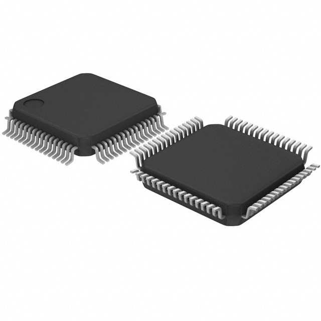
Pin Configuration
Figure 1. TQFP (Top View)
Document Number: 001-45652 Rev. *B
Page 4 of 25
[+] Feedback
�CY7C4205/CY7C4215 CY7C4225/CY7C4245
Selection Guide
Description Maximum frequency (MHz) Maximum access time (ns) Minimum cycle time (ns) Minimum data or enable set-up (ns) Minimum data or enable hold (ns) Maximum flag delay (ns) Operating current (ICC2) (mA) @ 20MHz Commercial Industrial Parameter Density Packages CY7C4205 256 x 18 64-pin TQFP (14 x 14, 10 x 10) CY7C4215 512 x 18 64-pin TQFP (14 x 14, 10 x 10) -10 100 8 10 3 0.5 8 45 50 CY7C4225 1K x 18 64-pin TQFP (14 x 14, 10 x 10) -15 66.7 10 15 4 1 10 45 50 CY7C4245 4K x 18 64-pin TQFP (14 x 14, 10 x 10)
Pin Definitions
Signal Name D017 Q017 WEN REN WCLK RCLK Description Data inputs Data outputs Write enable Read enable Write clock Read clock IO I O I I I I Data inputs for an 18-bit bus. Data outputs for an 18-bit bus. Enables the WCLK input. Enables the RCLK input. The rising edge clocks data into the FIFO when WEN is LOW and the FIFO is not Full. When LD is asserted, WCLK writes data into the programmable flag-offset register. The rising edge clocks data out of the FIFO when REN is LOW and the FIFO is not Empty. When LD is asserted, RCLK reads data out of the programmable flag-offset register. Dual-mode pin. Single device or width expansion - Half Full status flag. Cascaded – Write Expansion Out signal, connected to WXI of next device. When EF is LOW, the FIFO is empty. EF is synchronized to RCLK. When FF is LOW, the FIFO is full. FF is synchronized to WCLK. When PAE is LOW, the FIFO is almost empty based on the almost empty offset value programmed into the FIFO. PAE is asynchronous when VCC/SMODE is tied to VCC; it is synchronized to RCLK when V CC/SMODE is tied to VSS. When PAF is LOW, the FIFO is almost full based on the almost full offset value programmed into the FIFO. PAF is asynchronous when VCC/SMODE is tied to VCC; it is synchronized to WCLK when V CC/SMODE is tied to VSS. When LD is LOW, D017 (O017) are written (read) into (from) the programmable-flag-offset register. Dual-mode pin. Cascaded – The first device in the daisy chain will have FL tied to VSS; all other devices will have FL tied to VCC. In standard mode of width expansion, FL is tied to VSS on all devices. Not Cascaded – Tied to VSS. Retransmit function is also available in standalone mode by strobing RT. Cascaded – Connected to WXO of previous device. Not cascaded – Tied to VSS. Cascaded – Connected to RXO of previous device. Not cascaded – Tied to VSS. Function
WXO/HF EF FF PAE
Write expansion out/half full flag Empty flag Full flag Programmable almost empty Programmable almost full Load First load/ retransmit
O O O O
PAF
O
LD FL/RT
I I
WXI RXI
Write expansion input Read expansion input
I I
Document Number: 001-45652 Rev. *B
Page 5 of 25
[+] Feedback
�CY7C4205/CY7C4215 CY7C4225/CY7C4245
Pin Definitions (continued)
Signal Name RXO RS OE VCC/SMODE Description Read expansion output Reset Output enable Synchronous almost empty/ almost full flags IO O I I I Function Cascaded – Connected to RXI of next device. Resets device to empty condition. A reset is required before an initial read or write operation after power-up. When OE is LOW, the FIFO’s data outputs drive the bus to which they are connected. If OE is HIGH, the FIFO’s outputs are in High Z (high-impedance) state. Dual-Mode Pin. Asynchronous Almost Empty/Almost Full flags – tied to VCC. Synchronous Almost Empty/Almost Full flags – tied to VSS. (Almost Empty synchronized to RCLK, Almost Full synchronized to WCLK.)
Architecture
The CY7C42X5 consists of an array of 256 to 1 K words & 4 K words of 18 bits each (implemented by a dual-port array of SRAM cells), a read pointer, a write pointer, control signals (RCLK, WCLK, REN, WEN, RS), and flags (EF, PAE, HF, PAF, FF). The CY7C42X5 also includes the control signals WXI, RXI, WXO, RXO for depth expansion.
Programming
The CY7C42X5 devices contain two 12-bit offset registers. Data present on D0–11 during a program write will determine the distance from Empty (Full) that the Almost Empty (Almost Full) flags become active. If the user elects not to program the FIFO’s flags, the default offset values are used (see Table 2). When the Load LD pin is set LOW and WEN is set LOW, data on the inputs D0–11 is written into the Empty offset register on the first LOW-to-HIGH transition of the write clock (WCLK). When the LD pin and WEN are held LOW then data is written into the Full offset register on the second LOW-to-HIGH transition of the Write Clock (WCLK). The third transition of the Write Clock (WCLK) again writes to the Empty offset register (see Table 1). Writing all offset registers does not have to occur at one time. One or two offset registers can be written and then, by bringing the LD pin HIGH, the FIFO is returned to normal read/write operation. When the LD pin is set LOW, and WEN is LOW, the next offset register in sequence is written. The contents of the offset registers can be read on the output lines when the LD pin is set LOW and REN is set LOW; then, data can be read on the LOW-to-HIGH transition of the Read Clock (RCLK). Table 1. Write Offset Register LD 0 WEN 0 WCLK[1] Selection Writing to offset registers: Empty Offset Full Offset No operation
Resetting the FIFO
Upon power-up, the FIFO must be reset with a Reset (RS) cycle. This causes the FIFO to enter the Empty condition signified by EF being LOW. All data outputs go LOW after the falling edge of RS only if OE is asserted. In order for the FIFO to reset to its default state, a falling edge must occur on RS and the user must not read or write while RS is LOW.
FIFO Operation
When the WEN signal is active (LOW), data present on the D0-17 pins is written into the FIFO on each rising edge of the WCLK signal. Similarly, when the REN signal is active LOW, data in the FIFO memory will be presented on the Q017 outputs. New data will be presented on each rising edge of RCLK while REN is active LOW and OE is LOW. REN must set up tENS before RCLK for it to be a valid read function. WEN must occur tENS before WCLK for it to be a valid write function. An Output Enable (OE) pin is provided to three-state the Q0–17 outputs when OE is deasserted. When OE is enabled (LOW), data in the output register will be available to the Q017 outputs after tOE. If devices are cascaded, the OE function will only output data on the FIFO that is read enabled. The FIFO contains overflow circuitry to disallow additional writes when the FIFO is full, and underflow circuitry to disallow additional reads when the FIFO is empty. An empty FIFO maintains the data of the last valid read on its Q017 outputs even after additional reads occur.
0
1
1
0
Write into FIFO
1
1
No operation
Note 1. The same selection sequence applies to reading from the registers. REN is enabled and read is performed on the LOW-to-HIGH transition of RCLK.
Document Number: 001-45652 Rev. *B
Page 6 of 25
[+] Feedback
�CY7C4205/CY7C4215 CY7C4225/CY7C4245
Flag Operation
The CY7C42X5 devices provide five flag pins to indicate the condition of the FIFO contents. Empty and Full are synchronous. PAE and PAF are synchronous if VCC/SMODE is tied to VSS. that the FIFO is either Almost Full or Almost Empty. See Table 2 for a description of programmable flags. When the SMODE pin is tied LOW, the PAF flag signal transition is caused by the rising edge of the write clock and the PAE flag transition is caused by the rising edge of the read clock.
Full Flag
The Full Flag (FF) will go LOW when device is Full. Write operations are inhibited whenever FF is LOW regardless of the state of WEN. FF is synchronized to WCLK, i.e., it is exclusively updated by each rising edge of WCLK.
Retransmit
The retransmit feature is beneficial when transferring packets of data. It enables the receipt of data to be acknowledged by the receiver and retransmitted if necessary. The Retransmit (RT) input is active in the standalone and width expansion modes. The retransmit feature is intended for use when a number of writes equal to or less than the depth of the FIFO have occurred since the last RS cycle. A HIGH pulse on RT resets the internal read pointer to the first physical location of the FIFO. WCLK and RCLK may be free running but must be disabled during and tRTR after the retransmit pulse. With every valid read cycle after retransmit, previously accessed data is read and the read pointer is incremented until it is equal to the write pointer. Flags are governed by the relative locations of the read and write pointers and are updated during a retransmit cycle. Data written to the FIFO after activation of RT are transmitted also. The full depth of the FIFO can be repeatedly retransmitted.
Empty Flag
The Empty Flag (EF) will go LOW when the device is empty. Read operations are inhibited whenever EF is LOW, regardless of the state of REN. EF is synchronized to RCLK, i.e., it is exclusively updated by each rising edge of RCLK.
Programmable Almost Empty/Almost Full Flag
The CY7C42X5 features programmable Almost Empty and Almost Full Flags. Each flag can be programmed (described in the Programming section) a specific distance from the corresponding boundary flags (Empty or Full). When the FIFO contains the number of words or fewer for which the flags have been programmed, the PAF or PAE will be asserted, signifying Table 2. Flag Truth Table Number of Words in FIFO CY7C4205 - 256 x 18 0 1 to n[2] (n + 1) to 128 129 to (256 (m + 1)) (256 256 m)[] to 255 0 1 to n[2] (n + 1) to 256 257 to (512 (m + 1)) (512 m) to 511 512 Number of Words in FIFO CY7C4225 - 1K x 18 0 1 to n[2] (n + 1) to 512 513 to (1024 (m + 1)) (1024 m)[3] to 1023 1024 0 1 to n[2] (n + 1) to 2048 2049 to (4096 (m + 1)) (4096 m)[3] to 4095 4096 CY7C4245 - 4K x 18
[]
CY7C4215 - 512 x 18
FF H H H H H L
PAF H H H H L L
HF H H H L L L
PAE L L H H H H
EF L H H H H H
FF H H H H H L
PAF H H H H L L
HF H H H L L L
PAE L L H H H H
EF L H H H H H
Notes 2. n = Empty Offset (Default Values: CY7C4205 n = 31, CY7C4215 n = 63, CY7C4225/CY7C4245 n = 127). 3. m = Full Offset (Default Values: CY7C4205 n = 31, CY7C4215 n = 63, CY7C4225/CY7C4245 n = 127).
Document Number: 001-45652 Rev. *B
Page 7 of 25
[+] Feedback
�CY7C4205/CY7C4215 CY7C4225/CY7C4245
Width Expansion Configuration
The CY7C42X5 can be expanded in width to provide word widths greater than 18 in increments of 18. During width expansion mode all control line inputs are common and all flags are available. Empty (Full) flags should be created by ANDing the Empty (Full) flags of every FIFO. This technique will avoid ready data from the FIFO that is “staggered” by one clock cycle due to the variations in skew between RCLK and WCLK. Figure 2 demonstrates a 36-word width by using two CY7C42X5.
Figure 2. Block Diagram of Synchronous FIFO Memories Used in a Width Expansion Configuration RESET (RS) DATAIN (D) 36
18 18
RESET (RS) READ CLOCK (RCLK) READ ENABLE (REN) OUTPUT ENABLE(OE)
WRITE CLOCK (WCLK) WRITE ENABLE (WEN) LOAD (LD) PROGRAMMABLE(PAE) HALF FULL FLAG (HF) FF FULL FLAG (FF)
7C4205 7C4215 7C4225 7C4245 7C4205 7C4215 7C4225 7C4245
PROGRAMMABLE(PAF)
EMPTYFLAG (EF) EF
18
EF
18
FF
DATAOUT (Q)
36
FIRST LOAD (FL) WRITE EXPANSION IN (WXI) READ EXPANSION IN (RXI)
FIRST LOAD (FL) WRITE EXPANSION IN (WXI) READ EXPANSION IN (RXI)
Depth Expansion Configuration (with Programmable Flags)
The CY7C42X5 can easily be adapted to applications requiring more than 256/512/1024/4096 words of buffering. Figure 3 shows Depth Expansion using three CY7C42X5s. Maximum depth is limited only by signal loading. Follow these steps: 1. The first device must be designated by grounding the First Load (FL) control input. 2. All other devices must have FL in the HIGH state. 3. The Write Expansion Out (WXO) pin of each device must be tied to the Write Expansion In (WXI) pin of the next device. 4. The Read Expansion Out (RXO) pin of each device must be tied to the Read Expansion In (RXI) pin of the next device. 5. All Load (LD) pins are tied together. 6. The Half-Full Flag (HF) is not available in the Depth Expansion Configuration. 7. EF, FF, PAE, and PAF are created with composite flags by ORing together these respective flags for monitoring. The composite PAE and PAF flags are not precise.
Document Number: 001-45652 Rev. *B
Page 8 of 25
[+] Feedback
�CY7C4205/CY7C4215 CY7C4225/CY7C4245
Figure 3. Block Diagram of Synchronous FIFO Memory with Programmable Flags used in Depth Expansion Configuration
WXO RXO
FIRSTLOAD (FL)
VCC
7C4205 7C4215 7C4225 7C4245 FF EF PAE PAF WXI RXI
WXO RXO
DATAIN (D) VCC
7C4205 7C4215 7C4225 7C4245 FF EF PAE PAF WXI RXI
DATAOUT (Q)
FIRSTLOAD (FL)
WRITECLOCK (WCLK) WRITE ENABLE (WEN) RESET (RS)
WXO RXO
READ CLOCK (RCLK) READ ENABLE (REN)
LOAD (LD) FF PAF FF
7C4205 7C4215 7C4225 7C4245 EF
OUTPUT ENABLE (OE)
EF PAE
42X5–23
PAFWXI RXIPAE FIRSTLOAD (FL)
Document Number: 001-45652 Rev. *B
Page 9 of 25
[+] Feedback
�CY7C4205/CY7C4215 CY7C4225/CY7C4245
Maximum Ratings[6]
(Exceeding maximum ratings may shorten the useful life of the device. User guidelines are not tested) Storage temperature 65 C to +150 C Ambient temperature with power applied 55 C to +125 C Supply voltage to ground potential 0.5 V to +7.0 V DC voltage applied to outputs in High-Z state 0.5 V to +7.0 V DC input voltage 3.0 V to +7.0 V Output current into outputs (LOW) .............................. 20 mA Static discharge voltage ........................................... >2001 V (per MIL-STD-883, Method 3015) Latch-up current ...................................................... >200 mA
Operating Range
Range Commercial Industrial[4] Ambient Temperature 0 C to +70 C -40 C to +85 C -10 -15 Max 0.4 VCC 0.8 +10 +10 45 50 10 15 Min 2.4 2.2 3.0 10 90 10 Max 0.4 VCC 0.8 +10 +10 45 50 10 15 Unit V V V V A A A mA mA mA mA VCC 5 V ± 10% 5 V ± 10%
Electrical Characteristics Over the Operating Range[6]
Parameter VOH VOL VIH[7] VIL IIX IOS
[8] [7]
Description Output HIGH voltage Output LOW voltage Input HIGH voltage Input LOW voltage Input leakage current Output short circuit current Output OFF, High Z current Operating current Standby current
Test Conditions VCC = Min IOH = 2.0 mA VCC = Min IOL = 8.0 mA
Min 2.4 2.2 3.0
VCC = Max VCC = Max VOUT = GND OE > VIH, VSS < VO < VCC VCC = Max IOUT = 0 mA VCC = Max IOUT = 0 mA Com’l Ind’l Com’l Ind’l
10 90 10
IOZL IOZH ICC[9] ISB
[10]
Capacitance[11]
Parameter CIN COUT Description Input capacitance Output capacitance Test Conditions TA = 25 C, f = 1 MHz, VCC = 5.0 V Max 5 7 Unit pF pF
Notes 4. TA is the “instant on” case temperature. 5. See the last page of this specification for Group A subgroup testing information. 6. The Voltage on any input or I/O pin cannot exceed the power pin during power-up 7. The VIH and VIL specifications apply for all inputs except WXI, RXI. The WXI, RXI pin is not a TTL input. It is connected to either RXO, WXO of the previous device or VSS. 8. Test no more than one output at a time for not more than one second. 9. Input signals switch from 0 V to 3 V with a rise/fall time less than 3 ns, clocks and clock enables switch at 20 MHz, while the data inputs switch at 10 MHz. Outputs are unloaded. 10. All input signals are connected to VCC. All outputs are unloaded. 11. Tested initially and after any design or process changes that may affect these parameters.
Document Number: 001-45652 Rev. *B
Page 10 of 25
[+] Feedback
�CY7C4205/CY7C4215 CY7C4225/CY7C4245
Figure 4. AC Test Loads and Waveforms[12, 13]
R1 = 1.1 K 5V OUTPUT CL INCLUDING JIG AND SCOPE Equivalent to: THÉVENIN EQUIVALENT Rth = 410 OUTPUT Vth = 1.91 V R2 =680 3.0 V GND 3 ns
ALL INPUT PULSES
90% 10% 90% 10% 3 ns
Switching Characteristics Over the Operating Range
-10 Parameter tS tA tCLK tCLKH tCLKL tDS tDH tENS tENH tRS tRSR tRSF tPRT tRTR tOLZ tOE tOHZ tWFF tREF tPAFasynch tPAFsynch tPAEasynch tPAEsynch Description Clock cycle frequency Data access time Clock cycle time Clock HIGH time Clock LOW time. Data set-up time Data hold time Enable set-up time Enable hold time Reset pulse width[14] Reset recovery time Reset to flag and output time Retransmit pulse width Retransmit recovery time Output enable to output in low Z[15] Output enable to output valid Output enable to output in high Z[15] Write clock to full flag Read clock to empty flag Clock to programmable almost-full flag[16] (Asynchronous mode, VCC/SMODE tied to VCC) Clock to programmable almost-full flag (Synchronous mode, VCC/SMODE tied to VSS) Clock to programmable almost-empty flag[16] (Asynchronous mode, VCC/SMODE tied to VCC) Clock to programmable almost-full flag (Synchronous mode, VCC/SMODE tied to VSS) Min 2 10 4.5 4.5 3 0.5 3 0.5 10 8 12 12 0 3 3 Max 100 8 10 7 7 8 8 12 8 12 8 Min 2 15 6 6 4 1 4 1 15 10 15 15 0 3 3 -15 Max 66.7 10 15 8 8 10 10 16 10 16 10 Unit MHz ns ns ns ns ns ns ns ns ns ns ns ns ns ns ns ns ns ns ns ns ns ns
Notes 12. CL = 30 pF for all AC parameters except for tOHZ. 13. CL = 5 pF for tOHZ. 14. Pulse widths less than minimum values are not allowed. 15. Values guaranteed by design, not currently tested. 16. tPAFasynch, tPAEasynch, after program register write will not be valid until 5 ns + tPAF(E).
Document Number: 001-45652 Rev. *B
Page 11 of 25
[+] Feedback
�CY7C4205/CY7C4215 CY7C4225/CY7C4245
Switching Characteristics Over the Operating Range (continued)
-10 Parameter tHF tXO tXI tXIS tSKEW1 tSKEW2 tSKEW3 Description Clock to half-full flag Clock to expansion out Expansion in pulse width Expansion in set-up time Skew time between read clock and write clock for full flag Skew time between read clock and write clock for empty flag Skew time between read clock and write clock for programmable almost empty and programmable almost full flags. Min 3 4.5 5 5 10 Max 12 7 Min 6.5 5 6 6 15 -15 Max 16 10 Unit ns ns ns ns ns ns ns
Switching Waveforms
Figure 5. Write Cycle Timing
tCLK tCLKH WCLK tDS –D17 tENS WEN tWFF FF tSKEW1[17] RCLK tWFF tENH
NO OPERATION
tCLKL
tDH
REN
Note 17. tSKEW1 is the minimum time between a rising RCLK edge and a rising WCLK edge to guarantee that FF will go HIGH during the current clock cycle. If the time between the rising edge of RCLK and the rising edge of WCLK is less than tSKEW1, then FF may not change state until the next WCLK edge.
Document Number: 001-45652 Rev. *B
Page 12 of 25
[+] Feedback
�CY7C4205/CY7C4215 CY7C4225/CY7C4245
Switching Waveforms (continued)
Figure 6. Read Cycle Timing
tCLKH RCLK tENS REN tREF EF tA Q0–Q17 tOLZ OE tSKEW2 [18] WCLK tOE
VALID DATA
tCLK
tCLKL
tENH
NO OPERATION
tREF
tOHZ
WEN
Figure 7. Reset Timing[19]
tRS tRSR REN, WEN, LD tRSF EF,PAE tRSF FF,PAF, HF tRSF Q0–Q17 OE = 1 OE = 0
[20]
RS
Notes 18. tSKEW2 is the minimum time between a rising WCLK edge and a rising RCLK edge to guarantee that EF will go HIGH during the current clock cycle. It the time between the rising edge of WCLK and the rising edge of RCLK is less than tSKEW2, then EF may not change state until the next RCLK edge. 19. The clocks (RCLK, WCLK) can be free-running during reset. 20. After reset, the outputs will be LOW if OE = 0 and three-state if OE = 1.
Document Number: 001-45652 Rev. *B
Page 13 of 25
[+] Feedback
�CY7C4205/CY7C4215 CY7C4225/CY7C4245
Switching Waveforms (continued)
Figure 8. First Data Word Latency after Reset with Simultaneous Read and Write
WCLK tDS D0–D17 tENS WEN tSKEW2 RCLK tREF EF tFRL
[21]
D0 (FIRSTVALID WRITE)
D1
D2
D3
D4
REN tA Q0–Q17 tOLZ OE tOE tA [22] D0 D1
Figure 9. Empty Flag Timing
WCLK tDS D0–D17 tENS WEN tFRL[21] RCLK tSKEW2 EF REN OE tA Q0–Q17 D0 tREF tREF tSKEW2 tREF
[21] tFRL
tDS D0 tENH tENS D1 tENH
Notes 21. When tSKEW2 > minimum specification, tFRL (maximum) = tCLK + tSKEW2. When tSKEW2 < minimum specification, tFRL (maximum) = either 2*tCLK + tSKEW2 or tCLK + tSKEW2. The Latency Timing applies only at the Empty Boundary (EF = LOW). 22. The first word is available the cycle after EF goes HIGH, always.
Document Number: 001-45652 Rev. *B
Page 14 of 25
[+] Feedback
�CY7C4205/CY7C4215 CY7C4225/CY7C4245
Switching Waveforms (continued)
Figure 10. Full Flag Timing
NO WRITE WCLK tSKEW1 [17] D0–D17 tWFF FF tDS tSKEW1 [17] DATA WRITE tWFF tWFF DATA WRITE NO WRITE
WEN
RCLK tENS REN tENH tENS tENH
OE
LOW tA tA DATAREAD NEXT DATA READ
Q0–q17
DATA IN OUTPUT REGISTER
Figure 11. Half-Full Flag Timing
tCLKH WCLK tENS tENH WEN tHF HF HALF FULL OR LESS HALF FULL+1 OR MORE tHF RCLK tENS REN tCLKL
HALF FULL OR LESS
Note 23. tSKEW1 is the minimum time between a rising RCLK edge and a rising WCLK edge to guarantee that FF will go HIGH during the current clock cycle. If the time between the rising edge of RCLK and the rising edge of WCLK is less than tSKEW1, then FF may not change state until the next WCLK edge.
Document Number: 001-45652 Rev. *B
Page 15 of 25
[+] Feedback
�CY7C4205/CY7C4215 CY7C4225/CY7C4245
Switching Waveforms (continued)
Figure 12. Programmable Almost Empty Flag Timing
tCLKH WCLK tENS tENH WEN tPAE PAE
[24]
tCLKL
n+1WORDS IN FIFO tPAE
n WORDS IN FIFO
RCLK tENS REN
Figure 13. Programmable Almost Empty Flag Timing (applies only in SMODE (SMODE is LOW)
tCLKH WCLK tENS tENH WEN PAE tSKEW3 [26] RCLK tENS REN tENS tENH Note 25 tPAEsynch N + 1 WORDS INFIFO tCLKL
Note 27
tPAEsynch
Notes: 24. PAE offset n. Number of data words into FIFO already = n. 25. PAE offset n. 26. tSKEW3 is the minimum time between a rising WCLK and a rising RCLK edge for PAE to change state during that clock cycle. If the time between the edge of WCLK and the rising RCLK is less than tSKEW3, then PAE may not change state until the next RCLK. 27. If a read is performed on this rising edge of the read clock, there will be Empty + (n1) words in the FIFO when PAE goes LOW.
Document Number: 001-45652 Rev. *B
Page 16 of 25
[+] Feedback
�CY7C4205/CY7C4215 CY7C4225/CY7C4245
Switching Waveforms (continued)
Figure 14. Programmable Almost Full Flag Timing
tCLKH Note 28 WCLK tENS tENH WEN tPAF PAF
[29]
tCLKL
FULL M WORDS IN FIFO [30] tPAF
FULL M + 1 WORDS IN FIFO [31]
RCLK tENS REN
Figure 15. Programmable Almost Full Flag Timing (applies only in SMODE (SMODE in LOW))
tCLKH WCLK tENS tENH WEN Note 33 PAF FULL – M + 1 WORDS IN FIFO tPAF FULL M WORDS IN FIFO [30] tSKEW3 [34] tPAFsynch tCLKL Note 32
RCLK tENS REN tENS tENH
Notes: 28. PAF offset = m. Number of data words written into FIFO already = 64 m + 1 for the CY7C4205, 256 m + 1 for the CY7C4205, 512m + 1 for the CY7C4215. 1024 m + 1 for the CY7C4225, 2048 m + 1 for the CY7C4235, and 4096 m + 1 for the CY7C4245. 29. PAF is offset = m. 30. 64 m words in CY7C4205, 256 – m words in CY7C4205, 512 m words in CY7C4215. 1024 – m words in CY7C4225, 2048 m words in CY7C4235, and 4096 – m words in CY7C4245. 31. 64 m + 1 words in CY7C4205, 256 m + 1 words in CY7C4205, 512 m + 1 words in CY7C4215, 1024 m + 1 CY7C4225, 2048 m + 1 in CY7C4235, and 4096 m + 1 words in CY7C4245. 32. If a write is performed on this rising edge of the write clock, there will be Full – (m–1) words of the FIFO when PAF goes LOW. 33. PAF offset = m. 34. tSKEW3 is the minimum time between a rising RCLK and a rising WCLK edge for PAF to change state during that clock cycle. If the time between the edge of RCLK and the rising edge of WCLK is less than tSKEW3, then PAF may not change state until the next WCLK rising edge.
Document Number: 001-45652 Rev. *B
Page 17 of 25
[+] Feedback
�CY7C4205/CY7C4215 CY7C4225/CY7C4245
Switching Waveforms (continued)
Figure 16. Write Programmable Registers
tCLK tCLKH WCLK tENS LD tENS WEN tDS D0–D17 PAE OFFSET PAF OFFSET D0–D11 tDH PAE OFFSET tENH tCLKL
Figure 17. Read Programmable Registers
tCLK tCLKH RCLK tENS LD tENS REN tA Q0–Q17 UNKNOWN PAE OFFSET PAF OFFSET PAE OFFSET tENH tCLKL
Figure 18. Write Expansion Out Timing
tCLKH WCLK Note 35 tXO WXO tENS WEN tXO
Note: 35. Write to Last Physical Location.
Document Number: 001-45652 Rev. *B
Page 18 of 25
[+] Feedback
�CY7C4205/CY7C4215 CY7C4225/CY7C4245
Switching Waveforms (continued)
Figure 19. Read Expansion Out Timing
tCLKH RCLK Note 36 tXO RXO tENS REN tXO
Figure 20. Write Expansion In Timing
tXI WXI
WCLK
tXIS
Figure 21. Read Expansion In Timing
tXI RXI tXIS
RCLK
Figure 22. Retransmit Timing[37, 38, 39]
FL/RT tPRT tRTR REN/WEN
EF/FF and/all async flags HF/PAE/PAF
Notes: 36. Read from Last Physical Location. 37. Clocks are free running in this case. 38. The flags may change state during Retransmit as a result of the offset of the read and write pointers, but flags will be valid at tRTR. 39. For the synchronous PAE and PAF flags (SMODE), an appropriate clock cycle is necessary after tRTR to update these flags.
Document Number: 001-45652 Rev. *B
Page 19 of 25
[+] Feedback
�CY7C4205/CY7C4215 CY7C4225/CY7C4245
Figure 23. Typical AC and DC Characteristics
NORMALIZED SUPPLY CURRENT vs. SUPPLY VOLTAGE 1.4 NORMALIZED ICC NORMALIZED ICC 1.2 1.0 0.8 0.6 4 4.5 5 5.5 6 SUPPLY VOLTAGE (V) NORMALIZED tA vs.SUPPLY VOLTAGE 1.2 NORMALIZED tA TA =25 ° C NORMALIZED tA 1.1 1.0 0.9 0.8 1.50 1.25 1.0 .75 0.5 −55 VCC =5.0V NORMALIZED tA VIN =3.0V TA =25 ° C f=100 MHz 1.2 NORMALIZED ICC 1.1 1.0 0.9 0.8 −55 25 125 AMBIENT TEMPERATURE (° C) NORMALIZED tA vs. AMBIENT TEMPERATURE 40 VIN =3.0V VCC =5.0V f=100 MHz NORMALIZED SUPPLY CURRENT vs. AMBIENT TEMPERATURE NORMALIZED SUPPLY CURRENT vs. FREQUENCY 1.1 1.0 0.9 0.8 0.7 0.6 0 25 50 75 100
VCC =5.0V TA =25° C VIN =3.0V
FREQUENCY (MHz)
TYPICAL tA CHANGE vs. OUTPUT LOADING
25
10 VCC =5.0V TA =25° C 275 550 825 1000
4
4.5
5
5.5
6
25
125
−5.0 .50
SUPPLY VOLTAGE (V) OUTPUT SOURCECURRENT vs. OUTPUT VOLTAGE OUTPUT SINK CURENT (mA) 55 45 35 25 TA =25 ° C VCC =5.0V
AMBIENT TEMPERATURE (° C) OUTPUT SINK CURRENT vs. OUTPUT VOLTAGE 120 140 120 100 80 60 40 20 0 TA =25 ° C VCC =5.0V
CAPACITANCE (pF)
OUTPUTS OURCE CURRENT (mA)
0
1
2
3
4
5
0
1
2
3
4
OUTPUT VOLTAGE (V)
OUTPUT VOLTAGE (V)
Document Number: 001-45652 Rev. *B
Page 20 of 25
[+] Feedback
�CY7C4205/CY7C4215 CY7C4225/CY7C4245
Ordering Information
256 x 18 Synchronous FIFO Speed (ns) 10 Speed (ns) 15 Speed (ns) 10 15 Ordering Code CY7C4205-10AXC Package Name 51-85046 Package Name 51-85046 Package Name 51-85046 51-85046 51-85051 Package Name 51-85046 51-85046 51-85051 Package Type 64-Pin (14 x 14) Thin Quad Flatpack (Pb-Free) Package Type 64-Pin (14 x 14) Thin Quad Flatpack (Pb-Free) Package Type 64-Pin (14 x 14) Thin Quad Flatpack (Pb-Free) 64-Pin (14 x 14) Thin Quad Flatpack (Pb-Free) 64-Pin (10 x 10) Thin Quad Flatpack (Pb-Free) Package Type 64-Pin (14 x 14) Thin Quad Flatpack (Pb-Free) 64-Pin (14 x 14) Thin Quad Flatpack (Pb-Free) 64-Pin (10 x 10) Thin Quad Flatpack (Pb-Free) Operating Range Industrial Commercial Operating Range Commercial Operating Range Industrial Operating Range Industrial Commercial
512 x 18 Synchronous FIFO Ordering Code CY7C4215-15AXI
1K x 18 Synchronous FIFO Ordering Code CY7C4225-10AXI CY7C4225-15AXC CY7C4225-15ASXC 4K x 18 Synchronous FIFO Speed (ns) 10 15 Ordering Code CY7C4245-10AXI CY7C4245-15AXC CY7C4245-15ASXC
Ordering Code Definitions
CY
7
C
4
2X
5
XX
X
X
C, I
Temperature Grade: C = Commercial, I = Industrial
Pb-free (RoHS Compliant) Package: A = TQFP, AS = STQFP Speed grade: 10 ns or 15 ns x18
Depth: 20 = 256; 21 = 512 22 = 1 K; 24 = 4 K
FIFO Technology: CMOS
Family: Dual-port SRAM
Company ID: CY = Cypress
Document Number: 001-45652 Rev. *B
Page 21 of 25
[+] Feedback
�CY7C4205/CY7C4215 CY7C4225/CY7C4245
Package Diagrams
Figure 24. 64-Pin Thin Plastic Quad Flat Pack (14 x 14 x 1.4 mm), 51-85046
51-85046 *E
Document Number: 001-45652 Rev. *B
Page 22 of 25
[+] Feedback
�CY7C4205/CY7C4215 CY7C4225/CY7C4245
Package Diagrams (continued)
Figure 25. 64-Pin Thin Plastic Quad Flat Pack (10 x 10 x 1.4 mm), 51-85051
51-85051 *B
Acronyms
Acronym CMOS FIFO OE TQFP TTL first-in first-out output enable thin quad flat package Transistor-transistor logic Description Complementary metal oxide semiconductor
Document Conventions
Units of Measure
Symbol ns V µA mA mV mW MHz pF °C W nano seconds Volts micro Amperes milli Amperes milli Volts milli Watts Mega Hertz pico Farad degree Celcius Watts Unit of Measure
Document Number: 001-45652 Rev. *B
Page 23 of 25
[+] Feedback
�CY7C4205/CY7C4215 CY7C4225/CY7C4245
Document History Page
Document Title: CY7C4205/CY7C4215/CY7C4225/CY7C4245, 256/512/1K/4K x 18 Synchronous FIFOs Document Number: 001-45652 REV. ** *A ECN NO. 2489087 3094407 Issue Date See ECN 11/24/10 Orig. of Change VKN ADMU Description of Change This document is recreated from the existing pdf file on web. This is provided a new spec number. Removed following invalid parts from the ordering information table. CY7C4205-15AC CY7C4205-15AXC CY7C4215-15AI CY7C4225-10AI CY7C4225-15ASC CY7C4235-15AXC CY7C4245-10AI CY7C4245-10AXC CY7C4245-10ASXC CY7C4245-15JXC Added ordering code definitions. Updated package diagrams to latest revision. Removed obsolete part information. Removed 51-85005 package diagram. Updated package diagrams 51-85046. Title modified, Ordering code definition updated. Added Acronyms and Units of Measure table Removed PLCC figure from pin confirguration and the references.
*B
3264857
05/25/2011
ADMU
Document Number: 001-45652 Rev. *B
Page 24 of 25
[+] Feedback
�CY7C4205/CY7C4215 CY7C4225/CY7C4245
Sales, Solutions, and Legal Information
Worldwide Sales and Design Support
Cypress maintains a worldwide network of offices, solution centers, manufacturer’s representatives, and distributors. To find the office closest to you, visit us at Cypress Locations.
Products
Automotive Clocks & Buffers Interface Lighting & Power Control Memory Optical & Image Sensing PSoC Touch Sensing USB Controllers Wireless/RF cypress.com/go/automotive cypress.com/go/clocks cypress.com/go/interface cypress.com/go/powerpsoc cypress.com/go/plc cypress.com/go/memory cypress.com/go/image cypress.com/go/psoc cypress.com/go/touch cypress.com/go/USB cypress.com/go/wireless
PSoC Solutions
psoc.cypress.com/solutions PSoC 1 | PSoC 3 | PSoC 5
© Cypress Semiconductor Corporation, 2010-2011. The information contained herein is subject to change without notice. Cypress Semiconductor Corporation assumes no responsibility for the use of any circuitry other than circuitry embodied in a Cypress product. Nor does it convey or imply any license under patent or other rights. Cypress products are not warranted nor intended to be used for medical, life support, life saving, critical control or safety applications, unless pursuant to an express written agreement with Cypress. Furthermore, Cypress does not authorize its products for use as critical components in life-support systems where a malfunction or failure may reasonably be expected to result in significant injury to the user. The inclusion of Cypress products in life-support systems application implies that the manufacturer assumes all risk of such use and in doing so indemnifies Cypress against all charges. Any Source Code (software and/or firmware) is owned by Cypress Semiconductor Corporation (Cypress) and is protected by and subject to worldwide patent protection (United States and foreign), United States copyright laws and international treaty provisions. Cypress hereby grants to licensee a personal, non-exclusive, non-transferable license to copy, use, modify, create derivative works of, and compile the Cypress Source Code and derivative works for the sole purpose of creating custom software and or firmware in support of licensee product to be used only in conjunction with a Cypress integrated circuit as specified in the applicable agreement. Any reproduction, modification, translation, compilation, or representation of this Source Code except as specified above is prohibited without the express written permission of Cypress. Disclaimer: CYPRESS MAKES NO WARRANTY OF ANY KIND, EXPRESS OR IMPLIED, WITH REGARD TO THIS MATERIAL, INCLUDING, BUT NOT LIMITED TO, THE IMPLIED WARRANTIES OF MERCHANTABILITY AND FITNESS FOR A PARTICULAR PURPOSE. Cypress reserves the right to make changes without further notice to the materials described herein. Cypress does not assume any liability arising out of the application or use of any product or circuit described herein. Cypress does not authorize its products for use as critical components in life-support systems where a malfunction or failure may reasonably be expected to result in significant injury to the user. The inclusion of Cypress’ product in a life-support systems application implies that the manufacturer assumes all risk of such use and in doing so indemnifies Cypress against all charges. Use may be limited by and subject to the applicable Cypress software license agreement.
Document Number: 001-45652 Rev. *B
Revised May 25, 2011
Page 25 of 25
All products and company names mentioned in this document may be the trademarks of their respective holders.
[+] Feedback
�


 工商网监
湘ICP备2023018690号
工商网监
湘ICP备2023018690号
