Please note that Cypress is an Infineon Technologies Company.
The document following this cover page is marked as “Cypress” document as this is the
company that originally developed the product. Please note that Infineon will continue
to offer the product to new and existing customers as part of the Infineon product
portfolio.
Continuity of document content
The fact that Infineon offers the following product as part of the Infineon product
portfolio does not lead to any changes to this document. Future revisions will occur
when appropriate, and any changes will be set out on the document history page.
Continuity of ordering part numbers
Infineon continues to support existing part numbers. Please continue to use the
ordering part numbers listed in the datasheet for ordering.
www.infineon.com
�CY8C21334/CY8C21534
Automotive – Extended Temperature
PSoC® Programmable System-on-Chip™
Features
Pull-up, pull-down, high Z, strong, or open drain drive modes
on all GPIOs
❐ Analog input on all GPIOs
❐ Configurable interrupt on all GPIOs
Versatile analog mux
❐ Common internal analog bus
❐ Simultaneous connection of I/O combinations
Additional system resources
2
❐ Inter-Integrated Circuit (I C™) master, slave, or multi-master
operation up to 400 kHz
❐ Watchdog and sleep timers
❐ User-configurable low-voltage detection (LVD)
❐ Integrated supervisory circuit
❐ On-chip precision voltage reference
❐
Automotive Electronics Council (AEC) Q100 qualified
Powerful Harvard-architecture processor
❐ M8C processor speeds up to 12 MHz
❐ Low power at high speed
❐ Operating voltage: 4.75 V to 5.25 V
❐ Automotive temperature range: –40 °C to +125 °C
®
■ Advanced peripherals (PSoC blocks)
❐ Four analog Type E PSoC blocks provide:
• Two comparators with digital-to-analog converter (DAC)
references
• Up to 10-bit single or dual, 24 channel analog-to-digital
converters (ADC)
❐ Four digital PSoC blocks provide:
• 8- to 32-bit timers, counters, and pulse width modulators
(PWMs)
• Cyclical redundancy check (CRC) and pseudo-random
sequence (PRS) modules
• Full- or half-duplex UART
• SPI master or slave
• Connectable to all general purpose I/O (GPIO) pins
❐ Complex peripherals by combining blocks
• Capacitive sensing application capability
■
■
■
■
Logic Block Diagram
Flexible on-chip memory
❐ 8 KB flash program storage
❐ 512 bytes SRAM data storage
❐ In-system serial programming (ISSP)
❐ Partial flash updates
❐ Flexible protection modes
❐ EEPROM emulation in flash
■ Complete development tools
❐ Free development software (PSoC Designer™)
❐ Full-featured in-circuit emulator (ICE) and programmer
❐ Full-speed emulation
❐ Complex breakpoint structure
❐ 128 KB trace memory
■ Precision, programmable clocking
❐ Internal 24 MHz oscillator
❐ Internal low-speed, low-power oscillator for Watchdog and
Sleep functionality
❐ Optional external oscillator, up to 24 MHz
■ Programmable pin configurations
❐ 25 mA sink, 10 mA drive on all GPIOs
■
Cypress Semiconductor Corporation
Document Number: 38-12038 Rev. *M
•
198 Champion Court
•
San Jose, CA 95134-1709
•
408-943-2600
Revised December 7, 2017
�CY8C21334/CY8C21534
Contents
PSoC Functional Overview .............................................. 3
The PSoC Core ........................................................... 3
The Digital System ...................................................... 3
The Analog System ..................................................... 4
Additional System Resources ..................................... 4
PSoC Device Characteristics ...................................... 5
Getting Started .................................................................. 5
Application Notes ........................................................ 5
Development Kits ........................................................ 5
Training ....................................................................... 5
CYPros Consultants .................................................... 5
Solutions Library .......................................................... 5
Technical Support ....................................................... 5
Development Tools .......................................................... 6
PSoC Designer Software Subsystems ........................ 6
Designing with PSoC Designer ....................................... 7
Select Components ..................................................... 7
Configure Components ............................................... 7
Organize and Connect ................................................ 7
Generate, Verify, and Debug ....................................... 7
Pinouts .............................................................................. 8
20-pin Part Pinout ........................................................ 8
28-pin Part Pinout ........................................................ 9
Registers ......................................................................... 10
Register Conventions ................................................ 10
Register Mapping Tables .......................................... 10
Electrical Specifications ................................................ 13
Absolute Maximum Ratings ....................................... 14
Operating Temperature ............................................. 14
Document Number: 38-12038 Rev. *M
DC Electrical Characteristics ..................................... 15
AC Electrical Characteristics ..................................... 18
Packaging Information ................................................... 23
Thermal Impedances ................................................. 24
Solder Reflow Specifications ..................................... 24
Tape and Reel Information ........................................ 25
Development Tool Selection ......................................... 27
Software .................................................................... 27
Development Kits ...................................................... 27
Evaluation Tools ........................................................ 27
Device Programmers ................................................. 28
Accessories (Emulation and Programming) .............. 28
Ordering Information ...................................................... 29
Ordering Code Definitions ......................................... 29
Acronyms ........................................................................ 30
Reference Documents .................................................... 30
Document Conventions ................................................. 31
Units of Measure ....................................................... 31
Numeric Conventions .................................................... 31
Glossary .......................................................................... 31
Document History Page ................................................. 36
Sales, Solutions, and Legal Information ...................... 38
Worldwide Sales and Design Support ....................... 38
Products .................................................................... 38
PSoC® Solutions ...................................................... 38
Cypress Developer Community ................................. 38
Technical Support ..................................................... 38
Page 2 of 38
�CY8C21334/CY8C21534
PSoC Functional Overview
The PSoC family consists of many devices with on-chip
controllers. These devices are designed to replace multiple
traditional
microcontroller
unit
(MCU)-based
system
components with one, low-cost single-chip programmable
component. A PSoC device includes configurable blocks of
analog and digital logic, and programmable interconnect. This
architecture makes it possible for you to create customized
peripheral configurations, to match the requirements of each
individual application. Additionally, a fast central processing unit
(CPU), flash program memory, SRAM data memory, and
configurable I/O are included in a range of convenient pinouts.
The PSoC architecture, as illustrated in the Logic Block Diagram
on page 1, comprises of four main areas: the core, the system
resources, the digital system, and the analog system. Configurable global bus resources allow all the device resources to be
combined into a complete custom system. Each CY8C21x34
PSoC device includes four digital blocks and four analog blocks.
Depending on the PSoC package, up to 24 GPIOs are also
included. The GPIOs provide access to the global digital and
analog interconnects.
The PSoC Core
The PSoC core is a powerful engine that supports a rich
instruction set. It encompasses SRAM for data storage, an
interrupt controller, sleep, and watchdog timers, and an internal
main oscillator (IMO) and internal low-speed oscillator (ILO). The
CPU core, called the M8C, is a powerful processor with speeds
up to 12 MHz. The M8C is a two-million instructions per second
(MIPS) 8-bit Harvard-architecture microprocessor.
which are called user modules. Digital peripheral configurations
include those listed.
■
PWMs (8- to 32-bit)
■
PWMs with dead band (8- to 24-bit)
■
Counters (8- to 32-bit)
■
Timers (8- to 32-bit)
■
Full or half-duplex 8-bit UART with selectable parity
■
SPI master and slave
■
I2C master, slave, or multi-master (implemented in a dedicated
I2C block)
■
Cyclical redundancy checker/generator (16-bit)
■
Infrared Data Association (IrDA)
■
PRS generators (8- to 32-bit)
The digital blocks can be connected to any GPIO through a
series of global buses that can route any signal to any pin. The
buses also allow for signal multiplexing and for performing logic
operations. This configurability frees your designs from the
constraints of a fixed peripheral controller.
Figure 1. Digital System Block Diagram
Port 3
Digital Clocks
From Core
System resources provide additional capability, such as digital
clocks for increased flexibility, I2C functionality for implementing
an I2C master, slave, or multi-master, an internal voltage
reference that provides an absolute value of 1.3 V to a number
of PSoC subsystems, and various system resets supported by
the M8C.
The analog system is composed of four analog PSoC blocks,
supporting comparators and analog-to-digital conversion with up
to 10 bits of precision.
The Digital System
The digital system is composed of four digital PSoC blocks. Each
block is an 8-bit resource that can be used alone or combined
with other blocks to form 8-, 16-, 24-, and 32-bit peripherals,
Document Number: 38-12038 Rev. *M
Port 0
To Analog
System
To System Bus
DIGITAL SYSTEM
Row Input
Configuration
Digital PSoC Block Array
Row 0
DBB00
DBB01
DCB02
4
DCB03
4
8
Row Output
Configuration
The digital system is composed of an array of digital PSoC
blocks, which can be configured into any number of digital
peripherals. The digital blocks can be connected to the GPIO
through a series of global buses that can route any signal to any
pin. This frees designs from the constraints of a fixed peripheral
controller.
Port 1
Port 2
8
8
8
GIE[7:0]
GIO[7:0]
Global Digital
Interconnect
GOE[7:0]
GOO[7:0]
Digital blocks are provided in rows of four, where the number of
blocks varies by PSoC device family. This allows you the
optimum choice of system resources for your application. Family
resources are shown in Table 1 on page 5.
Page 3 of 38
�CY8C21334/CY8C21534
The Analog System
The Analog Multiplexer System
The analog system is composed of four configurable blocks,
allowing the creation of complex analog signal flows. Analog
peripherals are very flexible and can be customized to support
specific application requirements. Some of the common PSoC
analog functions for this device (most available as user modules)
are listed.
The analog mux bus can connect to every GPIO pin. Pins can
be connected to the bus individually or in any combination. The
bus also connects to the analog system for analysis with
comparators and ADCs. An additional 8:1 analog input
multiplexer provides a second path to bring Port 0 pins to the
analog array.
Switch-control logic enables selected pins to precharge
continuously under hardware control. This enables capacitive
measurement for applications such as touch sensing. Other
multiplexer applications include:
■
ADCs (single or dual, with up to 10-bit resolution)
■
Pin-to-pin comparator
■
Single-ended comparators (up to two) with absolute (1.3 V)
reference or 8-bit DAC reference
■
Track pad, finger sensing.
1.3 V reference (as a system resource)
■
Chip-wide mux that allows analog input from any I/O pin.
■
Crosspoint connection between any I/O pin combination.
■
In most PSoC devices, analog blocks are provided in columns of
three, which includes one continuous time (CT) and two switched
capacitor (SC) blocks. The CY8C21x34 devices provide limited
functionality type ‘E’ analog blocks. Each column contains one
CT type ‘E’ block and one SC type ‘E’ block. Refer to the PSoC
Programmable System-on-Chip Technical Reference Manual for
detailed information on the CY8C21x34’s type ‘E’ analog blocks.
Figure 2. Analog System Block Diagram
Additional System Resources
System resources, some of which have been previously listed,
provide additional capability useful for complete systems. Brief
statements describing the merits of each system resource are
presented.
■
From Port 0
■
Array Input
Configuration
ACI0[1:0]
ACI1[1:0]
The I2C module provides communication up to 400 kHz over
two wires. Slave, master, and multi-master modes are all
supported.
■
LVD interrupts can signal the application of falling voltage
levels, while the advanced power-on reset (POR) circuit
eliminates the need for a system supervisor.
■
An internal 1.3-V voltage reference provides an absolute
reference for the analog system, including ADCs and DACs.
■
Versatile analog multiplexer system
All IO
ACOL1MUX
Analog Mux Bus
Digital clock dividers provide three customizable clock
frequencies for use in applications. The clocks can be routed
to both the digital and analog systems. Additional clocks can
be generated using digital PSoC blocks as clock dividers.
Array
ACE00
ACE01
ASE10
ASE11
Document Number: 38-12038 Rev. *M
Page 4 of 38
�CY8C21334/CY8C21534
PSoC Device Characteristics
Depending on your PSoC device characteristics, the digital and analog systems can have a varying number of digital and analog
blocks. The following table lists the resources available for specific PSoC device groups. The PSoC device covered by this data sheet
is highlighted in Table 1.
Table 1. PSoC Device Characteristics
PSoC Part
Number
Digital
I/O
Digital
Rows
Digital
Blocks
Analog
Inputs
Analog
Outputs
Analog
Columns
Analog
Blocks
SRAM
Size
Flash
Size
CY8C29x66[1]
up to 64
4
16
up to 12
4
4
12
2K
32 K
CY8C28xxx
up to 44
up to 3
up to 12
up to 44
up to 4
up to 6
up to
12 + 4[2]
1K
16 K
CY8C27x43
up to 44
2
8
up to 12
4
4
12
256
16 K
CY8C24x94[1]
up to 56
1
4
up to 48
2
2
6
1K
16 K
CY8C24x23A
[1]
up to 24
1
4
up to 12
2
2
6
256
4K
CY8C23x33
up to 26
1
4
up to 12
2
2
4
256
8K
CY8C22x45[1]
up to 38
2
8
up to 38
0
4
6[2]
1K
16 K
[1]
up to 24
1
4
up to 24
0
4
6[2]
512
8K
CY8C21x34[1]
up to 28
1
4
up to 28
0
2
4[2]
512
8K
CY8C21x23
up to 16
1
4
up to 8
0
2
4[2]
256
4K
up to 28
0
0
up to 28
0
0
3[2,3]
512
8K
up to 36
0
0
up to 36
0
0
3[2,3]
up to 2 K
up to 32 K
CY8C21x45
CY8C20x34
[1]
CY8C20xx6
Getting Started
For in-depth information, along with detailed programming
details, see the PSoC® Technical Reference Manual.
CYPros Consultants
For up-to-date ordering, packaging, and electrical specification
information, see the latest PSoC device datasheets on the web.
Certified PSoC consultants offer everything from technical
assistance to completed PSoC designs. To contact or become a
PSoC consultant go to the CYPros Consultants web site.
Application Notes
Solutions Library
Cypress application notes are an excellent introduction to the
wide variety of possible PSoC designs.
Visit our growing library of solution focused designs. Here you
can find various application designs that include firmware and
hardware design files that enable you to complete your designs
quickly.
Development Kits
PSoC Development Kits are available online from and through a
growing number of regional and global distributors, which
include Arrow, Avnet, Digi-Key, Farnell, Future Electronics, and
Newark.
Training
Technical Support
Technical support – including a searchable Knowledge Base
articles and technical forums – is also available online. If you
cannot find an answer to your question, call our Technical
Support hotline at 1-800-541-4736.
Free PSoC technical training (on demand, webinars, and
workshops), which is available online via www.cypress.com,
covers a wide variety of topics and skill levels to assist you in
your designs.
Notes
1. Automotive qualified devices available in this group.
2. Limited analog functionality.
3. Two analog blocks and one CapSense® block.
Document Number: 38-12038 Rev. *M
Page 5 of 38
�CY8C21334/CY8C21534
Development Tools
PSoC Designer™ is the revolutionary integrated design
environment (IDE) that you can use to customize PSoC to meet
your specific application requirements. PSoC Designer software
accelerates system design and time to market. Develop your
applications using a library of precharacterized analog and digital
peripherals (called user modules) in a drag-and-drop design
environment. Then, customize your design by leveraging the
dynamically generated application programming interface (API)
libraries of code. Finally, debug and test your designs with the
integrated debug environment, including in-circuit emulation and
standard software debug features. PSoC Designer includes:
■
Application editor graphical user interface (GUI) for device and
user module configuration and dynamic reconfiguration
■
Extensive user module catalog
■
Integrated source-code editor (C and assembly)
■
Free C compiler with no size restrictions or time limits
■
Built-in debugger
■
In-circuit emulation
Built-in support for communication interfaces:
2
❐ Hardware and software I C slaves and masters
❐ Full-speed USB 2.0
❐ Up
to
four
full-duplex
universal
asynchronous
receiver/transmitters (UARTs), SPI master and slave, and
wireless
PSoC Designer supports the entire library of PSoC 1 devices and
runs on Windows XP, Windows Vista, and Windows 7.
■
PSoC Designer Software Subsystems
Design Entry
In the chip-level view, choose a base device to work with. Then
select different onboard analog and digital components that use
the PSoC blocks, which are called user modules. Examples of
user modules are ADCs, DACs, amplifiers, and filters. Configure
the user modules for your chosen application and connect them
to each other and to the proper pins. Then generate your project.
This prepopulates your project with APIs and libraries that you
can use to program your application.
The tool also supports easy development of multiple
configurations and dynamic reconfiguration. Dynamic
reconfiguration makes it possible to change configurations at run
time. In essence, this allows you to use more than 100 percent
of PSoC's resources for an application.
Document Number: 38-12038 Rev. *M
Code Generation Tools
The code generation tools work seamlessly within the
PSoC Designer interface and have been tested with a full range
of debugging tools. You can develop your design in C, assembly,
or a combination of the two.
Assemblers. The assemblers allow you to merge assembly
code seamlessly with C code. Link libraries automatically use
absolute addressing or are compiled in relative mode, and are
linked with other software modules to get absolute addressing.
C Language Compilers. C language compilers are available
that support the PSoC family of devices. The products allow you
to create complete C programs for the PSoC family devices. The
optimizing C compilers provide all of the features of C, tailored
to the PSoC architecture. They come complete with embedded
libraries providing port and bus operations, standard keypad and
display support, and extended math functionality.
Debugger
PSoC Designer has a debug environment that provides
hardware in-circuit emulation, allowing you to test the program in
a physical system while providing an internal view of the PSoC
device. Debugger commands allow you to read and program and
read and write data memory, and read and write I/O registers.
You can read and write CPU registers, set and clear breakpoints,
and provide program run, halt, and step control. The debugger
also allows you to create a trace buffer of registers and memory
locations of interest.
Online Help System
The online help system displays online, context-sensitive help.
Designed for procedural and quick reference, each functional
subsystem has its own context-sensitive help. This system also
provides tutorials and links to FAQs and an online support Forum
to aid the designer.
In-Circuit Emulator
A low-cost, high-functionality in-circuit emulator (ICE) is
available for development support. This hardware can program
single devices.
The emulator consists of a base unit that connects to the PC
using a USB port. The base unit is universal and operates with
all PSoC devices. Emulation pods for each device family are
available separately. The emulation pod takes the place of the
PSoC device in the target board and performs full-speed
(24 MHz) operation.
Page 6 of 38
�CY8C21334/CY8C21534
Designing with PSoC Designer
The development process for the PSoC device differs from that
of a traditional fixed function microprocessor. The configurable
analog and digital hardware blocks give the PSoC architecture a
unique flexibility that pays dividends in managing specification
change during development and by lowering inventory costs.
These configurable resources, called PSoC Blocks, have the
ability to implement a wide variety of user-selectable functions.
The PSoC development process can be summarized in the
following four steps:
1. Select User Modules
2. Configure User Modules
3. Organize and Connect
4. Generate, Verify, and Debug
Select Components
PSoC Designer provides a library of pre-built, pre-tested
hardware peripheral components called “user modules.” User
modules make selecting and implementing peripheral devices,
both analog and digital, simple.
Configure Components
Each of the User Modules you select establishes the basic
register settings that implement the selected function. They also
provide parameters and properties that allow you to tailor their
precise configuration to your particular application. For example,
a PWM User Module configures one or more
digital PSoC blocks, one for each 8 bits of resolution. The user
module parameters permit you to establish the pulse width and
duty cycle. Configure the parameters and properties to correspond to your chosen application. Enter values directly or by
selecting values from drop-down menus. All the user modules
are documented in datasheets that may be viewed directly in
PSoC Designer or on the Cypress website. These user module
datasheets explain the internal operation of the User Module and
Document Number: 38-12038 Rev. *M
provide performance specifications. Each datasheet describes
the use of each user module parameter, and other information
you may need to successfully implement your design.
Organize and Connect
You build signal chains at the chip level by interconnecting user
modules to each other and the I/O pins. You perform the
selection, configuration, and routing so that you have complete
control over all on-chip resources.
Generate, Verify, and Debug
When you are ready to test the hardware configuration or move
on to developing code for the project, you perform the “Generate
Configuration Files” step. This causes PSoC Designer to
generate source code that automatically configures the device to
your specification and provides the software for the system. The
generated code provides application programming interfaces
(APIs) with high-level functions to control and respond to
hardware events at run time and interrupt service routines that
you can adapt as needed.
A complete code development environment allows you to
develop and customize your applications in C, assembly
language, or both.
The last step in the development process takes place inside
PSoC Designer's Debugger (access by clicking the Connect
icon). PSoC Designer downloads the HEX image to the ICE
where it runs at full speed. PSoC Designer debugging capabilities rival those of systems costing many times more. In addition
to traditional single-step, run-to-breakpoint and watch-variable
features, the debug interface provides a large trace buffer and
allows you to define complex breakpoint events that include
monitoring address and data bus values, memory locations and
external signals.
Page 7 of 38
�CY8C21334/CY8C21534
Pinouts
The automotive CY8C21x34 PSoC device is available in a variety of packages which are listed and illustrated in the following tables.
Every port pin (labeled with a “P”) is capable of digital I/O and connection to the common analog bus. However, VSS, VDD, and XRES
are not capable of digital I/O.
20-pin Part Pinout
Table 2. 20-pin Part Pinout (SSOP)
Type
Pin
Name
No. Digital Analog
Description
1
I/O
I, M
P0[7]
Analog column mux input
2
I/O
I, M
P0[5]
Analog column mux input
3
I/O
I, M
P0[3]
Analog column mux input, CMOD capacitor pin
4
I/O
I, M
P0[1]
Analog column mux input, CMOD capacitor pin
VSS
Ground connection
5
Power
6
I/O
M
P1[7]
I2 C
7
I/O
M
P1[5]
I2C serial data (SDA)
8
I/O
M
P1[3]
9
I/O
M
P1[1]
I2C serial clock (SCL), ISSP-SCLK[4]
10
Power
serial clock (SCL)
VSS
Ground connection
11
I/O
M
P1[0]
I2C serial data (SDA), ISSP-SDATA[4]
12
I/O
M
P1[2]
13
I/O
M
P1[4]
14
I/O
M
P1[6]
15
Input
XRES
Active high external reset with internal
pull-down
I/O
I, M
P0[0]
Analog column mux input
17
I/O
I, M
P0[2]
Analog column mux input
18
I/O
I, M
P0[4]
Analog column mux input
19
I/O
I, M
P0[6]
Analog column mux input
VDD
Supply voltage
Power
AI, M, P0[7] 1
AI, M, P0[5] 2
AI, M, P0[3] 3
AI, M, P0[1] 4
VSS 5
I2C SCL, M, P1[7] 6
I2C SDA, M, P1[5] 7
M, P1[3] 8
I2C SCL, M, P1[1] 9
VSS 10
SSOP
20
19
18
17
16
15
14
13
12
11
VDD
P0[6], M, AI
P0[4], M, AI
P0[2], M, AI
P0[0], M, AI
XRES
P1[6], M
P1[4], M, EXTCLK
P1[2], M
P1[0], M, I2C SDA
Optional external clock (EXTCLK) input
16
20
Figure 3. CY8C21334 20-Pin PSoC Device
LEGEND A = Analog, I = Input, O = Output, and M = Analog Mux Input.
Note
4. These are the ISSP pins, which are not high Z when coming out of POR. See the PSoC Technical Reference Manual for details.
Document Number: 38-12038 Rev. *M
Page 8 of 38
�CY8C21334/CY8C21534
28-pin Part Pinout
Table 3. 28-pin Part Pinout (SSOP)
Type
Pin
No.
Digital
Analog
1
I/O
I, M
P0[7]
Analog column mux input
2
I/O
I, M
P0[5]
Analog column mux input
3
I/O
I, M
P0[3]
Analog column mux input, CMOD capacitor pin
4
I/O
I, M
P0[1]
Analog column mux input, CMOD capacitor pin
5
I/O
M
P2[7]
6
I/O
M
P2[5]
7
I/O
M
P2[3]
8
I/O
M
P2[1]
9
Power
Name
VSS
Description
Ground connection
10
I/O
M
P1[7]
I2C serial clock (SCL)
11
I/O
M
P1[5]
I2C serial data (SDA)
12
I/O
M
P1[3]
13
I/O
M
P1[1]
14
Power
VSS
15
I/O
M
P1[0]
16
I/O
M
P1[2]
17
I/O
M
P1[4]
18
I/O
M
P1[6]
19
Input
I2C serial clock (SCL), ISSP-SCLK[5]
AI, M, P0[7]
AI, M, P0[5]
AI, M, P0[3]
AI, M, P0[1]
M, P2[7]
M, P2[5]
M, P2[3]
M, P2[1]
VSS
I2C SCL, M, P1[7]
I2C SDA, M, P1[5]
M, P1[3]
I2C SCL, M, P1[1]
VSS
1
2
3
4
5
6
7
8
9
10
11
12
13
14
SSOP
28
27
26
25
24
23
22
21
20
19
18
17
16
15
VDD
P0[6], M, AI
P0[4], M, AI
P0[2], M, AI
P0[0], M, AI
P2[6], M
P2[4], M
P2[2], M
P2[0], M
XRES
P1[6], M
P1[4], M, EXTCLK
P1[2], M
P1[0], M, I2C SDA
Ground connection
I2C serial data (SDA), ISSP-SDATA[5]
Optional external clock (EXTCLK) input
XRES Active high external reset with internal
pull-down
20
I/O
M
P2[0]
21
I/O
M
P2[2]
22
I/O
M
P2[4]
23
I/O
M
P2[6]
24
I/O
I, M
P0[0]
Analog column mux input
25
I/O
I, M
P0[2]
Analog column mux input
26
I/O
I, M
P0[4]
Analog column mux input
27
I/O
I, M
P0[6]
Analog column mux input
VDD
Supply voltage
28
Figure 4. CY8C21534 28-pin PSoC Device
Power
LEGEND A = Analog, I = Input, O = Output, and M = Analog Mux Input.
Note
5. These are the ISSP pins, which are not high Z when coming out of POR. See the PSoC Technical Reference Manual for details.
Document Number: 38-12038 Rev. *M
Page 9 of 38
�CY8C21334/CY8C21534
Registers
Register Conventions
Register Mapping Tables
This section lists the registers of the automotive CY8C21x34
PSoC device. For detailed register information, reference the
PSoC Technical Reference Manual.
The PSoC device has a total register address space of
512 bytes. The register space is referred to as I/O space and is
divided into two banks. The XIO bit in the Flag register (CPU_F)
determines which bank the user is currently in. When the XIO bit
is set the user is in Bank 1.
The register conventions specific to this section are listed in
Table 4.
Table 4. Register Conventions
Convention
R
Note In the following register mapping tables, blank fields are
Reserved and must not be accessed.
Description
Read register or bit(s)
W
Write register or bit(s)
L
Logical register or bit(s)
C
Clearable register or bit(s)
#
Access is bit specific
Document Number: 38-12038 Rev. *M
Page 10 of 38
�CY8C21334/CY8C21534
Table 5. Register Map 0 Table: User Space
Name
PRT0DR
PRT0IE
PRT0GS
PRT0DM2
PRT1DR
PRT1IE
PRT1GS
PRT1DM2
PRT2DR
PRT2IE
PRT2GS
PRT2DM2
Addr (0,Hex) Access
Name
00
RW
01
RW
02
RW
03
RW
04
RW
05
RW
06
RW
07
RW
08
RW
09
RW
0A
RW
0B
RW
0C
0D
0E
0F
10
11
12
13
14
15
16
17
18
19
1A
1B
1C
1D
1E
1F
DBB00DR0
20
#
AMX_IN
DBB00DR1
21
W
AMUX_CFG
DBB00DR2
22
RW
PWM_CR
DBB00CR0
23
#
DBB01DR0
24
#
CMP_CR0
DBB01DR1
25
W
DBB01DR2
26
RW
CMP_CR1
DBB01CR0
27
#
DCB02DR0
28
#
ADC0_CR
DCB02DR1
29
W
ADC1_CR
DCB02DR2
2A
RW
DCB02CR0
2B
#
DCB03DR0
2C
#
TMP_DR0
DCB03DR1
2D
W
TMP_DR1
DCB03DR2
2E
RW
TMP_DR2
DCB03CR0
2F
#
TMP_DR3
30
31
32
ACE00CR1
33
ACE00CR2
34
35
36
ACE01CR1
37
ACE01CR2
38
39
3A
3B
3C
3D
3E
3F
Blank fields are Reserved and must not be accessed.
Document Number: 38-12038 Rev. *M
Addr (0,Hex)
40
41
42
43
44
45
46
47
48
49
4A
4B
4C
4D
4E
4F
50
51
52
53
54
55
56
57
58
59
5A
5B
5C
5D
5E
5F
60
61
62
63
64
65
66
67
68
69
6A
6B
6C
6D
6E
6F
70
71
72
73
74
75
76
77
78
79
7A
7B
7C
7D
7E
7F
Access
RW
RW
RW
#
RW
#
#
RW
RW
RW
RW
RW
RW
RW
RW
Name
ASE10CR0
Addr (0,Hex)
80
81
82
83
ASE11CR0
84
85
86
87
88
89
8A
8B
8C
8D
8E
8F
90
91
92
93
94
95
96
97
98
99
9A
9B
9C
9D
9E
9F
A0
A1
A2
A3
A4
A5
A6
A7
A8
A9
AA
AB
AC
AD
AE
AF
RDI0RI
B0
RDI0SYN
B1
RDI0IS
B2
RDI0LT0
B3
RDI0LT1
B4
RDI0RO0
B5
RDI0RO1
B6
B7
B8
B9
BA
BB
BC
BD
BE
BF
# Access is bit specific.
Access
RW
Name
RW
CUR_PP
STK_PP
IDX_PP
MVR_PP
MVW_PP
I2C_CFG
I2C_SCR
I2C_DR
I2C_MSCR
INT_CLR0
INT_CLR1
INT_CLR3
INT_MSK3
INT_MSK0
INT_MSK1
INT_VC
RES_WDT
DEC_CR0
DEC_CR1
RW
RW
RW
RW
RW
RW
RW
CPU_F
DAC_D
CPU_SCR1
CPU_SCR0
Addr (0,Hex)
C0
C1
C2
C3
C4
C5
C6
C7
C8
C9
CA
CB
CC
CD
CE
CF
D0
D1
D2
D3
D4
D5
D6
D7
D8
D9
DA
DB
DC
DD
DE
DF
E0
E1
E2
E3
E4
E5
E6
E7
E8
E9
EA
EB
EC
ED
EE
EF
F0
F1
F2
F3
F4
F5
F6
F7
F8
F9
FA
FB
FC
FD
FE
FF
Access
RW
RW
RW
RW
RW
RW
#
RW
#
RW
RW
RW
RW
RW
RW
RC
W
RW
RW
RL
RW
#
#
Page 11 of 38
�CY8C21334/CY8C21534
Table 6. Register Map 1 Table: Configuration Space
Name
PRT0DM0
PRT0DM1
PRT0IC0
PRT0IC1
PRT1DM0
PRT1DM1
PRT1IC0
PRT1IC1
PRT2DM0
PRT2DM1
PRT2IC0
PRT2IC1
Addr (1,Hex) Access
Name
00
RW
01
RW
02
RW
03
RW
04
RW
05
RW
06
RW
07
RW
08
RW
09
RW
0A
RW
0B
RW
0C
0D
0E
0F
10
11
12
13
14
15
16
17
18
19
1A
1B
1C
1D
1E
1F
DBB00FN
20
RW
CLK_CR0
DBB00IN
21
RW
CLK_CR1
DBB00OU
22
RW
ABF_CR0
23
AMD_CR0
DBB01FN
24
RW
CMP_GO_EN
DBB01IN
25
RW
DBB01OU
26
RW
AMD_CR1
27
ALT_CR0
DCB02FN
28
RW
DCB02IN
29
RW
DCB02OU
2A
RW
2B
CLK_CR3
DCB03FN
2C
RW
TMP_DR0
DCB03IN
2D
RW
TMP_DR1
DCB03OU
2E
RW
TMP_DR2
2F
TMP_DR3
30
31
32
ACE00CR1
33
ACE00CR2
34
35
36
ACE01CR1
37
ACE01CR2
38
39
3A
3B
3C
3D
3E
3F
Blank fields are Reserved and must not be accessed.
Document Number: 38-12038 Rev. *M
Addr (1,Hex)
40
41
42
43
44
45
46
47
48
49
4A
4B
4C
4D
4E
4F
50
51
52
53
54
55
56
57
58
59
5A
5B
5C
5D
5E
5F
60
61
62
63
64
65
66
67
68
69
6A
6B
6C
6D
6E
6F
70
71
72
73
74
75
76
77
78
79
7A
7B
7C
7D
7E
7F
Access
RW
RW
RW
RW
RW
RW
RW
RW
RW
RW
RW
RW
RW
RW
RW
RW
Name
ASE10CR0
Addr (1,Hex)
80
81
82
83
ASE11CR0
84
85
86
87
88
89
8A
8B
8C
8D
8E
8F
90
91
92
93
94
95
96
97
98
99
9A
9B
9C
9D
9E
9F
A0
A1
A2
A3
A4
A5
A6
A7
A8
A9
AA
AB
AC
AD
AE
AF
RDI0RI
B0
RDI0SYN
B1
RDI0IS
B2
RDI0LT0
B3
RDI0LT1
B4
RDI0RO0
B5
RDI0RO1
B6
B7
B8
B9
BA
BB
BC
BD
BE
BF
# Access is bit specific.
Access
RW
Name
RW
GDI_O_IN
GDI_E_IN
GDI_O_OU
GDI_E_OU
MUX_CR0
MUX_CR1
MUX_CR2
MUX_CR3
OSC_GO_EN
OSC_CR4
OSC_CR3
OSC_CR0
OSC_CR1
OSC_CR2
VLT_CR
VLT_CMP
ADC0_TR
ADC1_TR
IMO_TR
ILO_TR
BDG_TR
ECO_TR
RW
RW
RW
RW
RW
RW
RW
CPU_F
DAC_CR
CPU_SCR1
CPU_SCR0
Addr (1,Hex)
C0
C1
C2
C3
C4
C5
C6
C7
C8
C9
CA
CB
CC
CD
CE
CF
D0
D1
D2
D3
D4
D5
D6
D7
D8
D9
DA
DB
DC
DD
DE
DF
E0
E1
E2
E3
E4
E5
E6
E7
E8
E9
EA
EB
EC
ED
EE
EF
F0
F1
F2
F3
F4
F5
F6
F7
F8
F9
FA
FB
FC
FD
FE
FF
Access
RW
RW
RW
RW
RW
RW
RW
RW
RW
RW
RW
RW
RW
RW
RW
R
RW
RW
W
W
RW
W
RL
RW
#
#
Page 12 of 38
�CY8C21334/CY8C21534
Electrical Specifications
This section presents the DC and AC electrical specifications of the automotive CY8C21x34 PSoC device. For the most up to date
electrical specifications, confirm that you have the most recent datasheet by going to the web at http//www.cypress.com.
Specifications are valid for –40 C TA 125 C and TJ 135 C as specified, except where noted. Refer to Table 15 on page 18 for
the electrical specifications for the IMO using slow IMO (SLIMO) mode.
Figure 5. Voltage versus CPU Frequency
5.25
Figure 6. IMO Frequency Trim Options
lid ing
Va rat n
e io
Op eg
R
SLIMO
Mode=1
SLIMO
Mode=0
4.75
VDD Voltage (V)
VDD Voltage (V)
4.75
5.25
0
0
12 MHz
93 kHz
CPU Frequency
(nominal setting)
Document Number: 38-12038 Rev. *M
24 MHz
6 MHz
12 MHz
24 MHz
IMO Frequency
Page 13 of 38
�CY8C21334/CY8C21534
Absolute Maximum Ratings
Exceeding maximum ratings may shorten the useful life of the device. User guidelines are not tested.
Table 7. Absolute Maximum Ratings
Symbol
TSTG
Description
Storage temperature
TBAKETEMP Bake temperature
Min
Typ
Max
Units
Notes
–55
+25
+125
°C
Higher storage temperatures
reduce data retention time.
Recommended storage
temperature is +25 C ± 25 C.
Time spent in storage at a
temperature greater than 65 °C
counts toward the FlashDR
electrical specification in Table
14 on page 17.
Maximum combined storage
and operational time at +125 °C
is 7000 hours.
–
125
See
package
label
C
See
package
label
–
72
Hours
tBAKETIME
Bake time
TA
Ambient temperature with power applied
–40
–
+125
°C
VDD
Supply voltage on VDD relative to VSS
–0.5
–
+6.0
V
VIO
DC input voltage
VSS – 0.5
–
VDD + 0.5
V
VIOZ
DC voltage applied to tristate
VSS – 0.5
–
VDD + 0.5
V
IMIO
Maximum current into any port pin
–25
–
+50
mA
ESD
Electrostatic discharge (ESD) voltage
2000
–
–
V
LU
Latch-up current
–
–
200
mA
Min
Typ
Max
Units
Human body model ESD.
Operating Temperature
Table 8. Operating Temperature
Symbol
Description
TA
Ambient temperature
–40
–
+125
°C
TJ
Junction temperature
–40
–
+135
°C
Document Number: 38-12038 Rev. *M
Notes
The temperature rise from
ambient to junction is package
specific. See Table 22 on page 24.
The user must limit the power
consumption to comply with this
requirement.
Page 14 of 38
�CY8C21334/CY8C21534
DC Electrical Characteristics
DC Chip-Level Specifications
Table 9 lists guaranteed maximum and minimum specifications for the voltage and temperature ranges: 4.75 V to 5.25 V and
–40 °C TA 125 °C. Typical parameters apply to 5 V at 25 °C and are for design guidance only.
Table 9. DC Chip-Level Specifications
Symbol
Description
VDD
Supply voltage
IDD
Supply current, IMO = 24 MHz
ISB
ISBH
VREF
Sleep (mode) current with POR, LVD, sleep
timer, WDT, and ILO active. Mid temperature
range.
Sleep (mode) current with POR, LVD, sleep
timer, WDT, and ILO active. High temperature
range.
Reference voltage (Bandgap)
Min
4.75
–
Typ
–
4
Max
5.25
8
Units
Notes
V
See Table 13 on page 16.
mA Conditions are VDD = 5.25 V,
–40 °C TA 125 °C, CPU = 3
MHz, 48 MHz disabled. VC1 = 1.5
MHz, VC2 = 93.75 kHz, VC3 =
0.366 kHz.
–
5
12
A
VDD = 5.25 V, –40 C TA 55 °C.
–
5
100
A
VDD = 5.25 V, 55 C TA 125 °C.
1.25
1.30
1.35
V
DC GPIO Specifications
Table 10 lists guaranteed maximum and minimum specifications for the voltage and temperature ranges: 4.75 V to 5.25 V and
–40 °C TA 125 °C. Typical parameters apply to 5 V at 25 °C and are for design guidance only.
Table 10. DC GPIO Specifications
Symbol
Description
Min
Typ
Max
Units
Notes
RPU
Pull-up resistor
4
5.6
8
k
RPD
Pull-down resistor
4
5.6
8
k
Also applies to the internal
pull-down resistor on the XRES pin
VOH
High output level
3.5
–
–
V
IOH = 10 mA, VDD = 4.75 to 5.25 V
(8 total loads, 4 on even port pins
(for example, P0[2], P1[4]), 4 on odd
port pins (for example, P0[3],
P1[5])).
VOL
Low output level
–
–
0.75
V
IOL = 25 mA, VDD = 4.75 to 5.25 V
(8 total loads, 4 on even port pins
(for example, P0[2], P1[4]), 4 on odd
port pins (for example, P0[3],
P1[5])).
IOH
High level source current
10
–
–
mA
VOH VDD – 1.0 V, see the limitations of the total current in the note
for VOH.
IOL
Low level sink current
25
–
–
mA
VOL 0.75 V, see the limitations of
the total current in the note for VOL.
VIL
Input low level
–
–
0.8
V
VIH
Input high level
2.1
–
VH
Input hysteresis
–
60
–
mV
IIL
Input leakage (absolute value)
–
1
–
nA
Gross tested to 1 A.
CIN
Capacitive load on pins as input
–
3.5
10
pF
Package and pin dependent.
TA = 25 °C.
COUT
Capacitive load on pins as output
–
3.5
10
pF
Package and pin dependent.
TA = 25 °C.
Document Number: 38-12038 Rev. *M
V
Page 15 of 38
�CY8C21334/CY8C21534
DC Operational Amplifier Specifications
Table 11 lists guaranteed maximum and minimum specifications for the voltage and temperature ranges: 4.75 V to 5.25 V and
–40 °C TA 125 °C. Typical parameters apply to 5 V at 25 °C and are for design guidance only.
Table 11. DC Operational Amplifier Specifications
Symbol
VOSOA
Description
Input offset voltage (absolute value)
Min
Typ
Max
Units
–
2.5
15
mV
Notes
TCVOSOA Average input offset voltage drift
–
10
–
V/°C
IEBOA[6]
Input leakage current (Port 0 analog pins)
–
200
–
pA
Gross tested to 1 A.
CINOA
Input capacitance (Port 0 analog pins)
–
4.5
9.5
pF
Package and pin dependent.
TA = 25 °C.
VCMOA
Common mode voltage range
0.0
–
VDD – 1
V
GOLOA
Open loop gain
–
80
–
dB
ISOA
Amplifier supply current
–
10
100
A
DC Analog Mux Bus Specifications
Table 12 lists guaranteed maximum and minimum specifications for the voltage and temperature ranges: 4.75 V to 5.25 V and
–40 °C TA 125 °C. Typical parameters apply to 5 V at 25 °C and are for design guidance only.
Table 12. DC Analog Mux Bus Specifications
Symbol
Description
Min
Typ
Max
Units
RSW
Switch resistance to common analog bus
–
–
400
RVDD
Resistance of initialization switch to VDD
–
–
800
Notes
DC POR and LVD Specifications
Table 13 lists guaranteed maximum and minimum specifications for the voltage and temperature ranges: 4.75 V to 5.25 V and
–40 °C TA 125 °C. Typical parameters apply to 5 V at 25 °C and are for design guidance only.
Table 13. DC POR and LVD Specifications
Symbol
Description
VPPOR0
VPPOR1
VPPOR2
VDD value for PPOR trip
PORLEV[1:0] = 00b
PORLEV[1:0] = 01b
PORLEV[1:0] = 10b
VLVD0
VLVD1
VLVD2
VLVD3
VLVD4
VLVD5
VLVD6
VLVD7
VDD value for LVD trip
VM[2:0] = 000b
VM[2:0] = 001b
VM[2:0] = 010b
VM[2:0] = 011b
VM[2:0] = 100b
VM[2:0] = 101b
VM[2:0] = 110b
VM[2:0] = 111b
Min
Typ
Max
Units
Notes
VDD must be greater than or equal
to 2.5 V during startup, reset from
the XRES pin, or reset from
watchdog.
–
–
–
2.36
2.82
4.55
2.40
2.95
4.70
V
V
V
2.40
2.85
2.95
3.06
4.37
4.50
4.62
4.71
2.45
2.92
3.02
3.13
4.48
4.64
4.73
4.81
2.51[7]
2.99[8]
3.09
3.20
4.55
4.75
4.83
4.95
V
V
V
V
V
V
V
V
Notes
6. Atypical behavior: IEBOA of Port 0 Pin 0 is below 1 nA at 25 °C; 50 nA over temperature. Use Port 0 Pins 1-7 for the lowest leakage of 200 pA.
7. Always greater than 50 mV above VPPOR0 (PORLEV[1:0] = 00b) for falling supply.
8. Always greater than 50 mV above VPPOR1 (PORLEV[1:0] = 01b) for falling supply.
Document Number: 38-12038 Rev. *M
Page 16 of 38
�CY8C21334/CY8C21534
DC Programming Specifications
Table 14 lists guaranteed maximum and minimum specifications for the voltage and temperature ranges: 4.75 V to 5.25 V and
–40 °C TA 125 °C. Typical parameters apply to 5 V at 25 °C and are for design guidance only.
Table 14. DC Programming Specifications
Min
Typ
Max
Units
Notes
VDDP
Symbol
VDD for programming and erase
Description
4.5
5
5.5
V
This specification applies to the
functional requirements of external
programmer tools
VDDLV
Low VDD for verify
4.7
4.8
4.9
V
This specification applies to the
functional requirements of external
programmer tools
VDDHV
High VDD for verify
5.1
5.2
5.3
V
This specification applies to the
functional requirements of external
programmer tools
4.75
5.0
5.25
V
This specification applies to this
device when it is executing internal
flash writes
–
5
25
mA
VDDIWRITE Supply voltage for flash write operation
IDDP
Supply current during programming or verify
VILP
Input low voltage during programming or verify
–
–
0.8
V
VIHP
Input high voltage during programming or verify
2.2
–
–
V
IILP
Input current when applying VILP to P1[0] or
P1[1] during programming or verify
–
–
0.2
mA
Driving internal pull-down resistor.
IIHP
Input current when applying VIHP to P1[0] or
P1[1] during programming or verify
–
–
1.5
mA
Driving internal pull-down resistor.
VOLV
Output low voltage during programming or
verify
–
–
0.75
V
VOHV
Output high voltage during programming or
verify
3.5
–
VDD
V
FlashENPB Flash endurance (per block)[9]
FlashENT
FlashDR
Flash endurance (total)[9, 10]
Flash data
retention[11]
100
–
–
–
Erase/write cycles per block.
12,800
–
–
–
Erase/write cycles.
15
–
–
Years
Notes
9. For the full temperature range, the user must employ a temperature sensor user module (FlashTemp) or other temperature sensor, and feed the result to the
temperature argument before writing. Refer to the Flash APIs Application Note AN2015 for more information.
10. The maximum total number of allowed erase/write cycles is the minimum FlashENPB value multiplied by the number of flash blocks in the device.
11. Flash data retention based on the use condition of 7000 hours at TA 125 °C and the remaining time at TA 65 °C.
Document Number: 38-12038 Rev. *M
Page 17 of 38
�CY8C21334/CY8C21534
AC Electrical Characteristics
AC Chip-Level Specifications
Table 15 lists guaranteed maximum and minimum specifications for the voltage and temperature ranges: 4.75 V to 5.25 V and
–40 °C TA 125 °C. Typical parameters apply to 5 V at 25 °C and are for design guidance only.
Table 15. AC Chip-Level Specifications
Symbol
Description
Min
[12]
Typ
Max
[12]
Units
Notes
FIMO24
IMO frequency for 24 MHz
22.8
24
25.2
MHz Trimmed using factory trim
values. See Figure 6 on page 13.
SLIMO mode = 0.
FIMO6
IMO frequency for 6 MHz
5.5[12]
6
6.5[12]
MHz Trimmed using factory trim
values. See Figure 6 on page 13.
SLIMO mode = 1.
FCPU1
CPU frequency (5 V VDD nominal)
0.09[12]
12
12.6[12]
MHz SLIMO mode = 0.
0
24
25.2[12]
MHz Refer to Table 18 on page 20.
frequency0(5
FBLK5
Digital PSoC block
nominal)
V VDD
F32K1
ILO frequency
15
32
64
kHz
This specification applies when
the ILO has been trimmed.
F32KU
ILO untrimmed frequency
5
–
100
kHz
After a reset and before the M8C
processor starts to execute, the
ILO is not trimmed.
tXRST
External reset pulse width
10
–
–
s
DC24M
24 MHz duty cycle
40
50
60
%
DCILO
ILO duty cycle
20
50
80
%
Step24M
24 MHz trim step size
–
50
–
kHz
FMAX
Maximum frequency of signal on row input or
row output.
–
–
12.6[12]
MHz
SRPOWERUP Power supply slew rate
–
–
250
tPOWERUP
Time between end of POR state and CPU code
execution
–
16
100
ms
tJIT_IMO[13]
24 MHz IMO cycle-to-cycle jitter (RMS)
–
200
700
ps
24 MHz IMO long term N cycle-to-cycle jitter
(RMS)
–
300
900
24 MHz IMO period jitter (RMS)
–
100
400
V/ms VDD slew rate during power up.
Power-up from 0 V.
N = 32
Notes
12. Accuracy derived from Internal Main Oscillator with appropriate trim for VDD range.
13. Refer to Cypress Jitter Specifications document, Understanding Datasheet Jitter Specifications for Cypress Timing Products, for more information.
Document Number: 38-12038 Rev. *M
Page 18 of 38
�CY8C21334/CY8C21534
AC GPIO Specifications
Table 16 lists guaranteed maximum and minimum specifications for the voltage and temperature ranges: 4.75 V to 5.25 V and
–40 °C TA 125 °C. Typical parameters apply to 5 V at 25 °C and are for design guidance only.
Table 16. AC GPIO Specifications
Symbol
Description
Min
Typ
Max
Units
Notes
0
–
12.6[14]
MHz
Normal Strong Mode
FGPIO
GPIO operating frequency
tRISEF
Rise time, normal strong mode, Cload = 50 pF
2
–
22
ns
10% to 90%
tFALLF
Fall time, normal strong mode, Cload = 50 pF
2
–
22
ns
10% to 90%
tRISES
Rise time, slow strong mode, Cload = 50 pF
7
27
–
ns
10% to 90%
tFALLS
Fall time, slow strong mode, Cload = 50 pF
7
22
–
ns
10% to 90%
Figure 7. GPIO Timing Diagram
90%
GPIO
Pin
Output
Voltage
10%
tRISEF
tRISES
tFALLF
tFALLS
AC Operational Amplifier Specifications
Table 17 lists guaranteed maximum and minimum specifications for the voltage and temperature ranges: 4.75 V to 5.25 V and
–40 °C TA 125 °C. Typical parameters apply to 5 V at 25 °C and are for design guidance only.
Table 17. AC Operational Amplifier Specifications
Symbol
tCOMP
Description
Comparator mode response time, 50 mV
overdrive
Min
Typ
Max
Units
–
–
150
ns
Notes
Note
14. Accuracy derived from Internal Main Oscillator with appropriate trim for VDD range.
Document Number: 38-12038 Rev. *M
Page 19 of 38
�CY8C21334/CY8C21534
AC Digital Block Specifications
Table 18 lists guaranteed maximum and minimum specifications for the voltage and temperature ranges: 4.75 V to 5.25 V and
–40 °C TA 125 °C. Typical parameters apply to 5 V at 25 °C and are for design guidance only.
Table 18. AC Digital Block Specifications
Function
Description
All functions Block input clock frequency
Timer
Typ
Max
Units
–
–
25.2[16]
MHz
–
–
25.2[16]
MHz
MHz
Notes
Input clock frequency
No capture
With capture
Capture pulse width
Counter
Min
–
–
25.2[16]
50[15]
–
–
ns
–
–
25.2[16]
MHz
MHz
Input clock frequency
No enable input
–
–
25.2[16]
50[15]
–
–
ns
Asynchronous restart mode
20
–
–
ns
Synchronous restart mode
50[15]
–
–
ns
Disable mode
50[15]
–
–
ns
MHz
With enable input
Enable input pulse width
Dead Band Kill pulse width
Input clock frequency
–
–
25.2[16]
CRCPRS
Input clock frequency
(PRS Mode)
–
–
25.2[16]
MHz
CRCPRS
(CRC
Mode)
Input clock frequency
–
–
25.2[16]
MHz
SPIM
Input clock frequency
–
–
4.2[16]
MHz
The SPI serial clock (SCLK)
frequency is equal to the input
clock frequency divided by 2.
SPIS
Input clock (SCLK) frequency
–
–
2.1[16]
MHz
The input clock is the SPI SCLK in
SPIS mode.
50[15]
–
–
ns
Transmitter Input clock frequency
–
–
8.4[16]
MHz
The baud rate is equal to the input
clock frequency divided by 8.
Receiver
–
–
25.2[16]
MHz
The baud rate is equal to the input
clock frequency divided by 8.
Width of SS_ negated between
transmissions
Input clock frequency
Note
15. 50 ns minimum input pulse width is based on the input synchronizers running at 24 MHz (42 ns nominal period).
16. Accuracy derived from IMO with appropriate trim for VDD range.
Document Number: 38-12038 Rev. *M
Page 20 of 38
�CY8C21334/CY8C21534
AC External Clock Specifications
Table 19 lists guaranteed maximum and minimum specifications for the voltage and temperature ranges: 4.75 V to 5.25 V and
–40 °C TA 125 °C. Typical parameters apply to 5 V at 25 °C and are for design guidance only.
Table 19. AC External Clock Specifications
Symbol
FOSCEXT
Min
Typ
Max
Units
Frequency
Description
0.093
–
24.24
MHz
–
High period
20.6
–
5300
ns
–
Low period
20.6
–
–
ns
–
Power-up IMO to switch
150
–
–
s
Notes
AC Programming Specifications
Table 20 lists guaranteed maximum and minimum specifications for the voltage and temperature ranges: 4.75 V to 5.25 V and
–40 °C TA 125 °C. Typical parameters apply to 5 V at 25 °C and are for design guidance only.
Table 20. AC Programming Specifications
Symbol
Description
Min
Typ
Max
Units
1
–
20
ns
Fall time of SCLK
1
–
20
ns
Data setup time to falling edge of SCLK
40
–
–
ns
tHSCLK
Data hold time from falling edge of SCLK
40
–
–
ns
FSCLK
Frequency of SCLK
0
–
8
MHz
tERASEB
Flash erase time (block)
–
10
40[17]
ms
tWRITE
Flash block write time
–
40
160[17]
ms
tDSCLK
Data Out delay from falling edge of SCLK
–
–
50
ns
tPRGH
Total flash block program time
(tERASEB + tWRITE), hot
–
–
100[17]
ms
TJ 0 °C
tPRGC
Total flash block program time
(tERASEB + tWRITE), cold
–
–
200[17]
ms
TJ 0 °C
tRSCLK
Rise time of SCLK
tFSCLK
tSSCLK
Notes
Note
17. For the full temperature range, the user must employ a temperature sensor user module (FlashTemp) or other temperature sensor, and feed the result to the
temperature argument before writing. Refer to the Flash APIs Application Note AN2015 for more information.
Document Number: 38-12038 Rev. *M
Page 21 of 38
�CY8C21334/CY8C21534
AC I2C Specifications
Table 21 lists guaranteed maximum and minimum specifications for the voltage and temperature ranges: 4.75 V to 5.25 V and
–40 °C TA 125 °C. Typical parameters apply to 5 V at 25 °C and are for design guidance only.
Table 21. AC Characteristics of the I2C SDA and SCL Pins
Symbol
Standard Mode
Description
Fast Mode
Units
Min
Max
Min
Max
0
100[18]
0
400[18]
kHz
FSCLI2C
SCL clock frequency
tHDSTAI2C
Hold time (repeated) START condition. After
this period, the first clock pulse is generated.
4.0
–
0.6
–
s
tLOWI2C
LOW period of the SCL clock
4.7
–
1.3
–
s
tHIGHI2C
HIGH period of the SCL clock
4.0
–
0.6
–
s
tSUSTAI2C
Setup time for a repeated START condition
4.7
–
0.6
–
s
tHDDATI2C
Data hold time
0
–
0
–
s
tSUDATI2C
Data setup time
250
–
100[19]
–
ns
tSUSTOI2C
Setup time for STOP condition
4.0
–
0.6
–
s
tBUFI2C
Bus free time between a STOP and START
condition
4.7
–
1.3
–
s
tSPI2C
Pulse width of spikes are suppressed by the
input filter.
–
–
0
50
ns
Notes
Figure 8. Definition for Timing for Fast/Standard Mode on the I2C Bus
I2C_SDA
tSUDATI2C
tSPI2C
tHDDATI2C tSUSTAI2C
tHDSTAI2C
tBUFI2C
I2C_SCL
tHIGHI2C
S
START Condition
tLOWI2C
tSUSTOI2C
Sr
Repeated START Condition
P
S
STOP Condition
Notes
18. FSCLI2C is derived from SysClk of the PSoC. This specification assumes that SysClk is operating at 24 MHz, nominal. If SysClk is at a lower frequency, then the
FSCLI2C specification adjusts accordingly
19. A Fast-Mode I2C-bus device can be used in a Standard-Mode I2C-bus system, but the requirement tSUDATI2C 250 ns must then be met. This is automatically the
case if the device does not stretch the LOW period of the SCL signal. If such device does stretch the LOW period of the SCL signal, it must output the next data bit
to the SDA line trmax + tSUDATI2C = 1000 + 250 = 1250 ns (according to the Standard-Mode I2C-bus specification) before the SCL line is released.
Document Number: 38-12038 Rev. *M
Page 22 of 38
�CY8C21334/CY8C21534
Packaging Information
This section illustrates the packaging specifications for the automotive CY8C21x34 PSoC device, along with the thermal impedances
for each package.
Important Note Emulation tools may require a larger area on the target PCB than the chip’s footprint. For a detailed description of
the emulation tools' dimensions, refer to the emulator pod drawings at http://www.cypress.com.
Figure 9. 20-Pin SSOP (210 Mils)
51-85077 *F
Document Number: 38-12038 Rev. *M
Page 23 of 38
�CY8C21334/CY8C21534
Figure 10. 28-Pin SSOP (210 Mils)
51-85079 *F
Thermal Impedances
Solder Reflow Specifications
Table 22. Thermal Impedances per Package
Table 23 shows the solder reflow temperature limits that must not
be exceeded.
Package
20-pin SSOP
28-pin SSOP
Typical JA [20]
117 C/W
96 C/W
Typical JC
41 C/W
39 C/W
Table 23. Solder Reflow Specifications
Package
Maximum Peak
Temperature (TC)
Maximum Time
above TC – 5 °C
20-pin SSOP
260 C
30 seconds
28-pin SSOP
260 C
30 seconds
Note
20. TJ = TA + Power x JA
Document Number: 38-12038 Rev. *M
Page 24 of 38
�CY8C21334/CY8C21534
Tape and Reel Information
Figure 11. 20-Pin SSOP Carrier Tape Drawing
51-51101 *C
Document Number: 38-12038 Rev. *M
Page 25 of 38
�CY8C21334/CY8C21534
Figure 12. 28-Pin SSOP Carrier Tape Drawing
51-51100 *D
Table 24. Tape and Reel Specifications
Package
Cover Tape
Width (mm)
Hub Size
(inches)
Minimum Leading
Empty Pockets
20-pin SSOP
28-pin SSOP
13.3
13.3
4
7
42
42
Document Number: 38-12038 Rev. *M
Minimum
Trailing Empty
Pockets
25
25
Standard Full Reel
Quantity
2000
1000
Page 26 of 38
�CY8C21334/CY8C21534
Development Tool Selection
This section presents the development tools available for the automotive CY8C21x34 family.
Software
PSoC Designer
At the core of the PSoC development software suite is
PSoC Designer. Utilized by thousands of PSoC developers, this
robust software has been facilitating PSoC designs for years.
PSoC Designer
is
available
free
of
charge
at
http://www.cypress.com. PSoC Designer comes with a free C
compiler.
PSoC Programmer
Flexible enough to be used on the bench in development, yet
suitable for factory programming, PSoC Programmer works
either as a standalone programming application or it can operate
directly from PSoC Designer. PSoC Programmer software is
compatible with both PSoC ICE-Cube in-circuit emulator and
PSoC MiniProg. PSoC programmer is available free of charge at
http://www.cypress.com.
pre-defined control circuitry and plug-in hardware. The kit comes
with a control boards for CY8C20x34 and CY8C21x34 devices
as well as a breadboard module and a button(5)/slider module.
Evaluation Tools
All evaluation tools can be purchased from the Cypress Online
Store. The online store also has the most up to date information
on kit contents, descriptions, and availability.
CY3210-PSoCEval1
The CY3210-PSoCEval1 kit features an evaluation board and
the MiniProg1 programming unit. The evaluation board includes
an LCD module, potentiometer, LEDs, an RS-232 port, and
plenty of breadboarding space to meet all of your evaluation
needs. The kit includes:
■
Evaluation Board with LCD Module
■
MiniProg Programming Unit
Development Kits
■
28-Pin CY8C29466-24PXI PDIP PSoC Device Sample (2)
All development kits can be purchased from the Cypress Online
Store. The online store also has the most up to date information
on kit contents, descriptions, and availability.
■
PSoC Designer Software CD
■
Getting Started Guide
CY3215-DK Basic Development Kit
■
USB 2.0 Cable
The CY3215-DK is for prototyping and development with PSoC
Designer. This kit supports in-circuit emulation and the software
interface allows users to run, halt, and single step the processor
and view the contents of specific memory locations. Advanced
emulation features are also supported through PSoC Designer.
The kit includes:
CY3235-ProxDet
The CY3235-ProxDet CapSense Proximity Detection Demonstration Kit allows quick and easy demonstration of a PSoC
CapSense-enabled device (CY8C21x34) to accurately sense
the proximity of a hand or finger along the length of a wire
antenna. The kit includes:
■
ICE-Cube Unit
■
28-Pin PDIP Emulation Pod for CY8C29466-24PXI
■
28-Pin CY8C29466-24PXI PDIP PSoC Device Samples (two)
■
PSoC Designer Software CD
■
ISSP Cable
■
MiniEval Socket Programming and Evaluation board
■
Backward Compatibility Cable (for connecting to legacy Pods)
■
Universal 110/220 Power Supply (12 V)
■
European Plug Adapter
CY3210-21X34 Evaluation Pod (EvalPod)
■
USB 2.0 Cable
■
Getting Started Guide
■
Development Kit Registration form
PSoC EvalPods are pods that connect to the ICE In-Circuit
Emulator (CY3215-DK kit) to allow debugging capability. They
can also function as a standalone device without debugging
capability. The EvalPod has a 28-pin DIP footprint on the bottom
for easy connection to development kits or other hardware. The
top of the EvalPod has prototyping headers for easy connection
to the device’s pins. CY3210-21X34 provides evaluation of the
CY8C21x34 PSoC device family.
CY3280-BK1
The CY3280-BK1 Universal CapSense Control Kit is designed
for easy prototyping and debug of CapSense designs with
Document Number: 38-12038 Rev. *M
■
Proximity Detection Demo Board w/Antenna
■
I2C to USB Debugging/Communication Bridge
■
USB Cable (6 feet)
■
Supporting Software CD
■
CY3235-ProxDet Quick Start Guide
■
1 CY8C24894 PSoC device on I2C-USB Bridge
■
1 CY8C21434 PSoC device on Proximity Detection Demo
Board
Page 27 of 38
�CY8C21334/CY8C21534
Device Programmers
■
All device programmers can be purchased from the Cypress
Online Store. The online store also has the most up to date information on kit contents, descriptions, and availability.
CY3207ISSP In-System Serial Programmer (ISSP)
USB 2.0 Cable
CY3210-MiniProg1
The CY3207ISSP is a production programmer. It includes
protection circuitry and an industrial case that is more robust than
the MiniProg in a production-programming environment.
The CY3210-MiniProg1 kit allows a user to program PSoC
devices via the MiniProg1 programming unit. The MiniProg is a
small, compact prototyping programmer that connects to the PC
via a provided USB 2.0 cable. The kit includes:
Note: CY3207ISSP needs special software and is not
compatible with PSoC Programmer. This software is free and
can be downloaded from http://www.cypress.com. The kit
includes:
■
MiniProg Programming Unit
■
CY3207 Programmer Unit
■
MiniEval Socket Programming and Evaluation Board
■
PSoC ISSP Software CD
■
28-Pin CY8C29466-24PXI PDIP PSoC Device Sample
■
110 ~ 240 V Power Supply, Euro-Plug Adapter
■
PSoC Designer Software CD
■
USB 2.0 Cable
■
Getting Started Guide
Accessories (Emulation and Programming)
Table 25. Emulation and Programming Accessories
Part Number
Pin Package
Pod Kit[21]
Foot Kit[22]
CY8C21334-12PVXE
20-pin SSOP
CY3250-21X34
CY3250-20SSOP-FK
CY8C21534-12PVXE
28-pin SSOP
CY3250-21X34
CY3250-28SSOP-FK
Adapter[23]
Adapters can be found at
http://www.emulation.com.
Notes
21. Pod kit contains an emulation pod, a flex-cable (connects the pod to the ICE), two feet, and device samples.
22. Foot kit includes surface mount feet that can be soldered to the target PCB.
23. Programming adapter converts non-DIP package to DIP footprint. Specific details and ordering information for each of the adapters can be found at
http://www.emulation.com.
Document Number: 38-12038 Rev. *M
Page 28 of 38
�CY8C21334/CY8C21534
Ordering Information
The following table lists the automotive CY8C21x34 PSoC device’s key package features and ordering codes.
SRAM
(Bytes)
Temperature
Range
Digital
Blocks
Analog
Blocks
Digital I/O
Pins
Analog
Inputs
Analog
Outputs
XRES Pin
20-pin (210-Mil) SSOP
CY8C21334-12PVXE
8K
512
–40 C to +125 C
4
4
16
16
0
Yes
20-pin (210-Mil) SSOP
(tape and reel)
CY8C21334-12PVXET
8K
512
–40 C to +125 C
4
4
16
16
0
Yes
28-pin (210-Mil) SSOP
CY8C21534-12PVXE
8K
512
–40 C to +125 C
4
4
24
24
0
Yes
28-pin (210-Mil) SSOP
(tape and reel)
CY8C21534-12PVXET
8K
512
–40 C to +125 C
4
4
24
24
0
Yes
Package
Ordering
Code
Flash
(Bytes)
Table 26. PSoC Device Key Features and Ordering Information
Ordering Code Definitions
CY 8 C 21 xxx-12xx
Package Type:
PX = PDIP Pb-free
SX = SOIC Pb-free
PVX = SSOP Pb-free
LFX = QFN Pb-free
AX = TQFP Pb-free
Thermal Rating:
A = Automotive –40 °C to +85 °C
C = Commercial
I = Industrial
E = Automotive Extended –40 °C to +125 °C
CPU Speed: 12 MHz
Part Number
Family Code
Technology Code: C = CMOS
Marketing Code: 8 = PSoC
Company ID: CY = Cypress
Document Number: 38-12038 Rev. *M
Page 29 of 38
�CY8C21334/CY8C21534
Acronyms
The following table lists the acronyms that are used in this document.
Acronym
Description
Acronym
Description
AC
alternating current
MCU
microcontroller unit
ADC
analog-to-digital converter
MIPS
million instructions per second
API
application programming interface
PLL
phase-locked loop
AEC
Automotive Electronics Council
PDIP
plastic dual in-line package
CPU
central processing unit
POR
power-on reset
CT
continuous time
PPOR
precision POR
CRC
cyclic redundancy check
PCB
printed circuit board
DAC
digital-to-analog converter
PSoC®
Programmable System-on-Chip
DC
direct current or duty cycle
PRS
pseudo-random sequence
EEPROM
electrically erasable programmable read-only
memory
PWM
pulse-width modulator
EXTCLK
external clock
SCL /
SCLK
serial clock
XRES
external reset
SDA
serial data
GPIO
general-purpose I/O
SPI
serial peripheral interface
ICE
in-circuit emulator
SSOP
shrink small-outline package
IrDA
Infrared Data Association
SLIMO
slow IMO
I/O
input/output
SOIC
small-outline integrated circuit
ISSP
in-system serial programming
SRAM
static random-access memory
IDE
integrated development environment
SROM
supervisory read-only memory
I2C
Inter-Integrated Circuit
SMP
switch mode pump
ILO
internal low-speed oscillator
SC
switched capacitor
IMO
internal main oscillator
TQFP
thin quad flat pack
LED
light-emitting diode
UART
universal asynchronous receiver transmitter
LCD
liquid crystal display
USB
universal serial bus
LVD
low voltage detect
WDT
watchdog timer
Reference Documents
CY8CPLC20, CY8CLED16P01, CY8C29x66, CY8C27x43, CY8C24x94, CY8C24x23, CY8C24x23A, CY8C22x13, CY8C21x34,
CY8C21x23, CY7C64215, CY7C603xx, CY8CNP1xx, and CYWUSB6953 PSoC® Programmable System-on-Chip Technical
Reference Manual (TRM) (001-14463)
Design Aids – Reading and Writing PSoC® Flash – AN2015 (001-40459)
Understanding Datasheet Jitter Specifications for Cypress Timing Products
Document Number: 38-12038 Rev. *M
Page 30 of 38
�CY8C21334/CY8C21534
Document Conventions
Units of Measure
The following table lists the units of measure that are used in this document.
Symbol
Unit of Measure
Symbol
Unit of Measure
C
degree Celsius
ms
millisecond
dB
decibel
mV
millivolt
KB
1024 bytes
nA
nanoampere
Kbit
1024 bits
ns
nanosecond
kHz
kilohertz
W
ohm
k
kilohm
pA
picoampere
MHz
megahertz
pF
picofarad
A
microampere
ps
picosecond
s
microsecond
V
volt
V
microvolt
W
watt
mA
milliampere
Numeric Conventions
Hexadecimal numbers are represented with all letters in uppercase with an appended lowercase ‘h’ (for example, ‘14h’ or ‘3Ah’).
Hexadecimal numbers may also be represented by a ‘0x’ prefix, the C coding convention. Binary numbers have an appended
lowercase ‘b’ (for example, ‘01010100b’ or ‘01000011b’). Numbers not indicated by an ‘h’, ‘b’, or ‘0x’ are in decimal format.
Glossary
active high
1. A logic signal having its asserted state as the logic 1 state.
2. A logic signal having the logic 1 state as the higher voltage of the two states.
analog blocks
The basic programmable Opamp circuits. These are SC (switched capacitor) and CT (continuous time) blocks.
These blocks can be interconnected to provide ADCs, DACs, multi-pole filters, gain stages, and much more.
analog-to-digital
converter (ADC)
A device that changes an analog signal to a digital signal of corresponding magnitude. Typically, an ADC converts
a voltage to a digital number. The digital-to-analog converter (DAC) performs the reverse operation.
Application
programming
interface (API)
A series of software routines that comprise an interface between a computer application and lower level services
and functions (for example, user modules and libraries). APIs serve as building blocks for programmers that create
software applications.
asynchronous
A signal whose data is acknowledged or acted upon immediately, irrespective of any clock signal.
bandgap
reference
A stable voltage reference design that matches the positive temperature coefficient of VT with the negative
temperature coefficient of VBE, to produce a zero temperature coefficient (ideally) reference.
bandwidth
1. The frequency range of a message or information processing system measured in hertz.
2. The width of the spectral region over which an amplifier (or absorber) has substantial gain (or loss); it is
sometimes represented more specifically as, for example, full width at half maximum.
bias
1. A systematic deviation of a value from a reference value.
2. The amount by which the average of a set of values departs from a reference value.
3. The electrical, mechanical, magnetic, or other force (field) applied to a device to establish a reference level to
operate the device.
Document Number: 38-12038 Rev. *M
Page 31 of 38
�CY8C21334/CY8C21534
Glossary (continued)
block
1. A functional unit that performs a single function, such as an oscillator.
2. A functional unit that may be configured to perform one of several functions, such as a digital PSoC block or
an analog PSoC block.
buffer
1. A storage area for data that is used to compensate for a speed difference, when transferring data from one
device to another. Usually refers to an area reserved for I/O operations, into which data is read, or from which
data is written.
2. A portion of memory set aside to store data, often before it is sent to an external device or as it is received
from an external device.
3. An amplifier used to lower the output impedance of a system.
bus
1. A named connection of nets. Bundling nets together in a bus makes it easier to route nets with similar routing
patterns.
2. A set of signals performing a common function and carrying similar data. Typically represented using vector
notation; for example, address[7:0].
3. One or more conductors that serve as a common connection for a group of related devices.
clock
The device that generates a periodic signal with a fixed frequency and duty cycle. A clock is sometimes used to
synchronize different logic blocks.
comparator
An electronic circuit that produces an output voltage or current whenever two input levels simultaneously satisfy
predetermined amplitude requirements.
compiler
A program that translates a high level language, such as C, into machine language.
configuration
space
In PSoC devices, the register space accessed when the XIO bit, in the CPU_F register, is set to ‘1’.
crystal oscillator
An oscillator in which the frequency is controlled by a piezoelectric crystal. Typically a piezoelectric crystal is less
sensitive to ambient temperature than other circuit components.
cyclic redundancy A calculation used to detect errors in data communications, typically performed using a linear feedback shift
check (CRC)
register. Similar calculations may be used for a variety of other purposes such as data compression.
data bus
A bi-directional set of signals used by a computer to convey information from a memory location to the central
processing unit and vice versa. More generally, a set of signals used to convey data between digital functions.
debugger
A hardware and software system that allows you to analyze the operation of the system under development. A
debugger usually allows the developer to step through the firmware one step at a time, set break points, and
analyze memory.
dead band
A period of time when neither of two or more signals are in their active state or in transition.
digital blocks
The 8-bit logic blocks that can act as a counter, timer, serial receiver, serial transmitter, CRC generator,
pseudo-random number generator, or SPI.
digital-to-analog
converter (DAC)
A device that changes a digital signal to an analog signal of corresponding magnitude. The analog-to-digital
converter (ADC) performs the reverse operation.
duty cycle
The relationship of a clock period high time to its low time, expressed as a percent.
emulator
Duplicates (provides an emulation of) the functions of one system with a different system, so that the second
system appears to behave like the first system.
Document Number: 38-12038 Rev. *M
Page 32 of 38
�CY8C21334/CY8C21534
Glossary (continued)
external reset
(XRES)
An active high signal that is driven into the PSoC device. It causes all operation of the CPU and blocks to stop
and return to a pre-defined state.
flash
An electrically programmable and erasable, non-volatile technology that provides you the programmability and
data storage of EPROMs, plus in-system erasability. Non-volatile means that the data is retained when power is
off.
flash block
The smallest amount of flash ROM space that may be programmed at one time and the smallest amount of flash
space that may be protected.
frequency
The number of cycles or events per unit of time, for a periodic function.
gain
The ratio of output current, voltage, or power to input current, voltage, or power, respectively. Gain is usually
expressed in dB.
I2C
A two-wire serial computer bus by Phillips Semiconductors (now NXP Semiconductors). It is used to connect
low-speed peripherals in an embedded system. The original system was created in the early 1980s as a battery
control interface, but it was later used as a simple internal bus system for building control electronics. I2C uses
only two bi-directional pins, clock and data, both running at the VDD supply voltage and pulled high with resistors.
The bus operates up to100 kbits/second in standard mode and 400 kbits/second in fast mode.
ICE
The in-circuit emulator that allows you to test the project in a hardware environment, while viewing the debugging
device activity in a software environment (PSoC Designer).
input/output (I/O) A device that introduces data into or extracts data from a system.
interrupt
A suspension of a process, such as the execution of a computer program, caused by an event external to that
process, and performed in such a way that the process can be resumed.
interrupt service
routine (ISR)
A block of code that normal code execution is diverted to when the CPU receives a hardware interrupt. Many
interrupt sources may each exist with its own priority and individual ISR code block. Each ISR code block ends
with the RETI instruction, returning the device to the point in the program where it left normal program execution.
jitter
1. A misplacement of the timing of a transition from its ideal position. A typical form of corruption that occurs on
serial data streams.
2. The abrupt and unwanted variations of one or more signal characteristics, such as the interval between
successive pulses, the amplitude of successive cycles, or the frequency or phase of successive cycles.
low voltage detect A circuit that senses VDD and provides an interrupt to the system when VDD falls below a selected threshold.
(LVD)
M8C
An 8-bit Harvard-architecture microprocessor. The microprocessor coordinates all activity inside a PSoC by
interfacing to the flash, SRAM, and register space.
master device
A device that controls the timing for data exchanges between two devices. Or when devices are cascaded in
width, the master device is the one that controls the timing for data exchanges between the cascaded devices
and an external interface. The controlled device is called the slave device.
microcontroller
An integrated circuit chip that is designed primarily for control systems and products. In addition to a CPU, a
microcontroller typically includes memory, timing circuits, and I/O circuitry. The reason for this is to permit the
realization of a controller with a minimal quantity of chips, thus achieving maximal possible miniaturization. This
in turn, reduces the volume and the cost of the controller. The microcontroller is normally not used for
general-purpose computation as is a microprocessor.
mixed-signal
The reference to a circuit containing both analog and digital techniques and components.
Document Number: 38-12038 Rev. *M
Page 33 of 38
�CY8C21334/CY8C21534
Glossary (continued)
modulator
A device that imposes a signal on a carrier.
noise
1. A disturbance that affects a signal and that may distort the information carried by the signal.
2. The random variations of one or more characteristics of any entity such as voltage, current, or data.
oscillator
A circuit that may be crystal controlled and is used to generate a clock frequency.
parity
A technique for testing transmitted data. Typically, a binary digit is added to the data to make the sum of all the
digits of the binary data either always even (even parity) or always odd (odd parity).
phase-locked
loop (PLL)
An electronic circuit that controls an oscillator so that it maintains a constant phase angle relative to a reference
signal.
pinouts
The pin number assignment: the relation between the logical inputs and outputs of the PSoC device and their
physical counterparts in the printed circuit board (PCB) package. Pinouts involve pin numbers as a link between
schematic and PCB design (both being computer generated files) and may also involve pin names.
port
A group of pins, usually eight.
power-on reset
(POR)
A circuit that forces the PSoC device to reset when the voltage is below a pre-set level. This is one type of hardware
reset.
PSoC®
Cypress Semiconductor’s PSoC® is a registered trademark and Programmable System-on-Chip™ is a trademark
of Cypress.
PSoC Designer™ The software for Cypress’ Programmable System-on-Chip technology.
pulse width
An output in the form of duty cycle which varies as a function of the applied value.
modulator (PWM)
RAM
An acronym for random access memory. A data-storage device from which data can be read out and new data
can be written in.
register
A storage device with a specific capacity, such as a bit or byte.
reset
A means of bringing a system back to a known state. See hardware reset and software reset.
ROM
An acronym for read only memory. A data-storage device from which data can be read out, but new data cannot
be written in.
serial
1. Pertaining to a process in which all events occur one after the other.
2. Pertaining to the sequential or consecutive occurrence of two or more related activities in a single device or
channel.
settling time
The time it takes for an output signal or value to stabilize after the input has changed from one value to another.
shift register
A memory storage device that sequentially shifts a word either left or right to output a stream of serial data.
slave device
A device that allows another device to control the timing for data exchanges between two devices. Or when
devices are cascaded in width, the slave device is the one that allows another device to control the timing of data
exchanges between the cascaded devices and an external interface. The controlling device is called the master
device.
Document Number: 38-12038 Rev. *M
Page 34 of 38
�CY8C21334/CY8C21534
Glossary (continued)
SRAM
An acronym for static random access memory. A memory device where you can store and retrieve data at a high
rate of speed. The term static is used because, after a value is loaded into an SRAM cell, it remains unchanged
until it is explicitly altered or until power is removed from the device.
SROM
An acronym for supervisory read only memory. The SROM holds code that is used to boot the device, calibrate
circuitry, and perform flash operations. The functions of the SROM may be accessed in normal user code,
operating from flash.
stop bit
A signal following a character or block that prepares the receiving device to receive the next character or block.
synchronous
1. A signal whose data is not acknowledged or acted upon until the next active edge of a clock signal.
2. A system whose operation is synchronized by a clock signal.
tri-state
A function whose output can adopt three states: 0, 1, and Z (high-impedance). The function does not drive any
value in the Z state and, in many respects, may be considered to be disconnected from the rest of the circuit,
allowing another output to drive the same net.
UART
A UART or universal asynchronous receiver-transmitter translates between parallel bits of data and serial bits.
user modules
Pre-built, pre-tested hardware/firmware peripheral functions that take care of managing and configuring the lower
level analog and digital PSoC blocks. User modules also provide high level API (Application Programming
Interface) for the peripheral function.
user space
The bank 0 space of the register map. The registers in this bank are more likely to be modified during normal
program execution and not just during initialization. Registers in bank 1 are most likely to be modified only during
the initialization phase of the program.
VDD
A name for a power net meaning “voltage drain.” The most positive power supply signal. Usually 5 V or 3.3 V.
VSS
A name for a power net meaning “voltage source.” The most negative power supply signal.
watchdog timer
A timer that must be serviced periodically. If it is not serviced, the CPU resets after a specified period of time.
Document Number: 38-12038 Rev. *M
Page 35 of 38
�CY8C21334/CY8C21534
Document History Page
Document Title: CY8C21334/CY8C21534, Automotive – Extended Temperature PSoC® Programmable System-on-Chip™
Document Number: 38-12038
Revision
ECN
Orig. of
Change
Submission
Date
Description of Change
**
350496
HMT
04/18/05
New silicon and document (Revision **).
*A
395740
HMT
09/14/05
Update ISB and ISBH DC Chip-Level Specification notes for qual. Update
copyright, zip code, and CY Perform logo. Make data sheet Final.
*B
422602
HMT
02/03/06
Modify Storage Temperature and add recommended usage and related notes.
Update AC Chip-Level Spec., FCPU1. Add ISSP note to pinout tables.
Implement CY QFN standard. Add CY corporate address. Update trademarks.
*C
2101387
AESA
02/20/08
Post to www.cypress.com
*D
2641945
OGNE /
PYRS
01/21/09
Changed 25 mA Drive on All GPIO under Programmable Pin Configurations to
25 mA Sink, 10 mA Drive on All GPIO
Changed Analog-to-digital converters (single or dual, with 8-bit resolution)
under Analog-to-digital converters (single or dual, with up to 10-bit resolution)
Updated template.
Added Note in Ordering Information section.
Changed title from PSoC Mixed-Signal Array to PSoC
Programmable System-on-Chip
*E
2703345
VIVG /
PYRS
05/07/09
Updated Getting Started section. Replaced Designing with User Modules
section with Designing with PSoC Designer section. Updated Features list and
PSoC Functional Overview section. Updated some AC Specification values to
conform to a +/-4% accurate IMO (no order of magnitude changes). Added a
note to I2C specifications section to clarify the I2C SysClk dependency. Added
the Development Tool Selection section. Deleted some inapplicable or
redundant information. Changed the title. Updated the PDF Bookmarks.
*F
2822792
*G
2888007
BTK / AESA 12/07/2009 Added TPRGH, TPRGC, IOL, IOH, F32KU, DCILO, and TPOWERUP electrical specifications. Corrected the FlashENT electrical specification. Updated the text of
footnotes 6 and 7. Added maximum values and updated typical values for
TERASEB and TWRITE electrical specifications. Replaced TRAMP electrical specification with SRPOWERUP electrical specification. Added “Contents” on page 2.
NJF
Document Number: 38-12038 Rev. *M
03/30/2010 Updated Cypress website links.
Removed AC Analog Mux Bus Specifications.
Added TBAKETEMP and TBAKETIME parameters in Absolute Maximum Ratings
Updated Packaging Information.
Removed Third Party Tools and Build a PSoC Emulator into your Board.
Updated links in Sales, Solutions, and Legal Information.
Page 36 of 38
�CY8C21334/CY8C21534
Document History Page (continued)
Document Title: CY8C21334/CY8C21534, Automotive – Extended Temperature PSoC® Programmable System-on-Chip™
Document Number: 38-12038
Revision
ECN
Orig. of
Change
Submission
Date
Description of Change
*H
3118809
BTK / NJF
08/11/2011
Updated I2C timing diagram to improve clarity.
Updated wording, formatting, and notes of the AC Digital Block Specifications
table to improve clarify.
Added VDDP, VDDLV, and VDDHV electrical specifications to give more information for programming the device.
Updated solder reflow temperature specifications to give more clarity.
Updated the jitter specifications.
Updated PSoC Device Characteristics table.
Updated the F32KU electrical specification.
Updated DC POR and LVD Specifications to add specs for all POR and LVD
levels.
Updated note for RPD electrical specification.
Updated note for the TSTG electrical specification to add more clarity.
Added Tape and Reel Information section.
Updated Reference Information Section.
Added FIMO6 electrical specification and Figure 6 on page 13.
Changed FIMO24 electrical specification to give it a ±5% frequency accuracy.
Updated FCPU1, FBLK5, FMAX, and FGPIO electrical specifications and all AC
Digital Block Specifications to support a ±5% accuracy oscillator.
*I
3523799
SMYU
*J
3904247
JICG
02/14/2013 Updated Packaging Information (Updated Tape and Reel Information (spec
51-51101 – Changed revision from *B to *C)).
*K
5166373
SNPR
03/08/2016 Updated Packaging Information:
spec 51-85077 – Changed revision from *E to *F.
spec 51-85079 – Changed revision from *E to *F.
Updated Tape and Reel Information:
spec 51-51100 – Changed revision from *C to *D.
Updated to new template.
Completing Sunset Review.
*L
5655080
SNPR
03/09/2017 Updated to new template.
Completing Sunset Review.
*M
5987147
AESATMP9
12/07/2017 Updated logo and copyright.
Document Number: 38-12038 Rev. *M
02/13/2012 Updated Tape and Reel Information (51-51100 and 51-51101)
Page 37 of 38
�CY8C21334/CY8C21534
Sales, Solutions, and Legal Information
Worldwide Sales and Design Support
Cypress maintains a worldwide network of offices, solution centers, manufacturer’s representatives, and distributors. To find the office
closest to you, visit us at Cypress Locations.
PSoC® Solutions
Products
ARM® Cortex® Microcontrollers
Automotive
cypress.com/arm
cypress.com/automotive
Clocks & Buffers
Interface
Internet of Things
Memory
cypress.com/clocks
cypress.com/interface
cypress.com/iot
cypress.com/memory
Microcontrollers
cypress.com/mcu
PSoC
cypress.com/psoc
Power Management ICs
Touch Sensing
USB Controllers
Wireless Connectivity
PSoC 1 | PSoC 3 | PSoC 4 | PSoC 5LP | PSoC 6
Cypress Developer Community
Forums | WICED IOT Forums | Projects | Video | Blogs |
Training | Components
Technical Support
cypress.com/support
cypress.com/pmic
cypress.com/touch
cypress.com/usb
cypress.com/wireless
© Cypress Semiconductor Corporation, 2005-2017. This document is the property of Cypress Semiconductor Corporation and its subsidiaries, including Spansion LLC ("Cypress"). This document,
including any software or firmware included or referenced in this document ("Software"), is owned by Cypress under the intellectual property laws and treaties of the United States and other countries
worldwide. Cypress reserves all rights under such laws and treaties and does not, except as specifically stated in this paragraph, grant any license under its patents, copyrights, trademarks, or other
intellectual property rights. If the Software is not accompanied by a license agreement and you do not otherwise have a written agreement with Cypress governing the use of the Software, then Cypress
hereby grants you a personal, non-exclusive, nontransferable license (without the right to sublicense) (1) under its copyright rights in the Software (a) for Software provided in source code form, to
modify and reproduce the Software solely for use with Cypress hardware products, only internally within your organization, and (b) to distribute the Software in binary code form externally to end users
(either directly or indirectly through resellers and distributors), solely for use on Cypress hardware product units, and (2) under those claims of Cypress's patents that are infringed by the Software (as
provided by Cypress, unmodified) to make, use, distribute, and import the Software solely for use with Cypress hardware products. Any other use, reproduction, modification, translation, or compilation
of the Software is prohibited.
TO THE EXTENT PERMITTED BY APPLICABLE LAW, CYPRESS MAKES NO WARRANTY OF ANY KIND, EXPRESS OR IMPLIED, WITH REGARD TO THIS DOCUMENT OR ANY SOFTWARE
OR ACCOMPANYING HARDWARE, INCLUDING, BUT NOT LIMITED TO, THE IMPLIED WARRANTIES OF MERCHANTABILITY AND FITNESS FOR A PARTICULAR PURPOSE. To the extent
permitted by applicable law, Cypress reserves the right to make changes to this document without further notice. Cypress does not assume any liability arising out of the application or use of any
product or circuit described in this document. Any information provided in this document, including any sample design information or programming code, is provided only for reference purposes. It is
the responsibility of the user of this document to properly design, program, and test the functionality and safety of any application made of this information and any resulting product. Cypress products
are not designed, intended, or authorized for use as critical components in systems designed or intended for the operation of weapons, weapons systems, nuclear installations, life-support devices or
systems, other medical devices or systems (including resuscitation equipment and surgical implants), pollution control or hazardous substances management, or other uses where the failure of the
device or system could cause personal injury, death, or property damage ("Unintended Uses"). A critical component is any component of a device or system whose failure to perform can be reasonably
expected to cause the failure of the device or system, or to affect its safety or effectiveness. Cypress is not liable, in whole or in part, and you shall and hereby do release Cypress from any claim,
damage, or other liability arising from or related to all Unintended Uses of Cypress products. You shall indemnify and hold Cypress harmless from and against all claims, costs, damages, and other
liabilities, including claims for personal injury or death, arising from or related to any Unintended Uses of Cypress products.
Cypress, the Cypress logo, Spansion, the Spansion logo, and combinations thereof, WICED, PSoC, CapSense, EZ-USB, F-RAM, and Traveo are trademarks or registered trademarks of Cypress in
the United States and other countries. For a more complete list of Cypress trademarks, visit cypress.com. Other names and brands may be claimed as property of their respective owners.
Document Number: 38-12038 Rev. *M
Revised December 7, 2017
Page 38 of 38
�
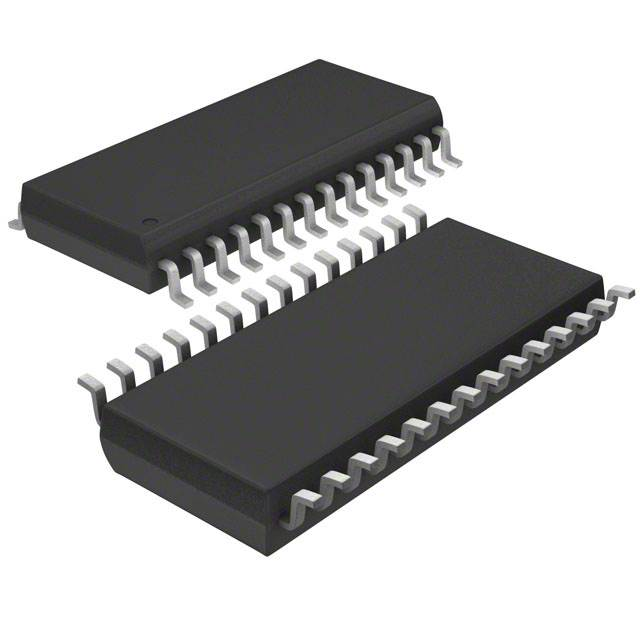


 工商网监
湘ICP备2023018690号
工商网监
湘ICP备2023018690号
