CYRF69303
Programmable Radio-on-Chip LPstar
Features
■
Operating temperature from 0 °C to 70 °C
■
Radio System-on-Chip with built-in 8-bit MCU in a single
device.
■
Closed-loop frequency synthesis for minimal frequency drift
■
Operates in the unlicensed worldwide Industrial, Scientific, and
Medical (ISM) band (2.400 GHz to 2.483 GHz).
■
Auto transaction sequencer (ATS): MCU can remain in sleep
state longer to save power
■
On Air compatible with second generation radio
WirelessUSB™ LP and PRoC LP.
■
Framing, length, CRC16, and Auto ACK
■
Pin-to-pin compatible with PRoC LP except the Pin31 and
Pin37.
■
Separate 16 byte transmit and receive FIFOs
■
Receive signal strength indication (RSSI)
■
Built-in serial peripheral interface (SPI) control while in Sleep
Mode
■
Advanced development tools based on Cypress’s PSoC® tools
■
Flexible I/O
■
2 mA source current on all GPIO pins. Configurable 8 mA or
50 mA/pin current sink on designated pins
■
Each GPIO pin supports high impedance inputs, configurable
pull up, open drain output, CMOS/TTL inputs, and CMOS
output
■
Maskable interrupts on all I/O pins
Simple Development
Intelligent
■
M8C based 8-bit CPU, optimized for human interface devices
(HID) applications
■
256 bytes of SRAM
■
8 Kbytes of flash memory with EEPROM emulation
■
In-system reprogrammable through D+/D– pins
■
CPU speed up to 12 MHz
■
16-bit free running timer
■
Low power wakeup timer
■
12-bit programmable interval timer with interrupts
■
Watchdog timer
Low Power
■
21 mA operating current (Transmit at –5 dBm)
■
Sleep current less than 1 A
■
Operating voltage from 2.7 V to 3.6 V DC
■
Fast startup and fast channel changes
■
Supports coin cell operated applications
BOM Savings
■
Low external component count
■
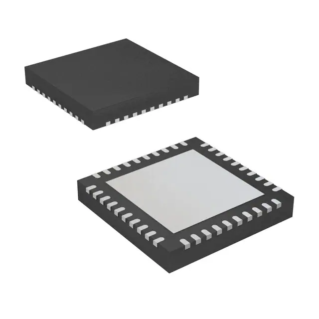
Small footprint 40-pin QFN (6 mm × 6 mm)
■
GPIOs that require no external components
■
Operates off a single crystal
Applications
■
Wireless keyboards and mice
■
Presentation tools
■
Wireless gamepads
■
Remote controls
■
Toys
■
Fitness
Reliable & Robust
■
■
Receive sensitivity typical –90 dBm
AutoRate™ - Dynamic Data Rate Reception
❐
❐
Enables data reception for any of the supported bit rates
automatically.
DSSS (250 Kbps), GFSK (1 Mbps)
Cypress Semiconductor Corporation
Document #: 001-66502 Rev. *B
•
198 Champion Court
•
San Jose, CA 95134-1709
•
408-943-2600
Revised February 28, 2012
�CYRF69303
nSS
VIO
VCC1
VCC2
VCC3
VCC4
VBat0
VBat1
VBat2
VCC
RST
VDD_MICRO
VCC
SCK
MOSI
Logic Block Diagram
RFbias
RFp
RFn
Microcontroller
Function
P0_1,3,4,7
4
Radio
Function
IRQ/GPIO
P1.5/MOSI
MISO/GPIO
P1.4/SCK
P1_0:2,6:7
5
XOUT/GPIO
P1.3/nSS
12 MHz
Document #: 001-66502 Rev. *B
Vdd
.....
GND
GND
RESV
Xtal
GND
P2_0:1
2
.......
Page 2 of 66
�CYRF69303
Contents
Functional Description ..................................................... 4
Functional Overview ........................................................ 4
2.4 GHz Radio Function .............................................. 4
Data Transmission Modes ........................................... 4
Microcontroller Function .............................................. 4
Backward Compatibility ............................................... 4
Pinouts .............................................................................. 5
Functional Block Overview .............................................. 6
2.4 GHz Radio ............................................................. 6
Frequency Synthesizer ................................................ 6
Baseband and Framer ................................................. 6
Packet Buffers and Radio Configuration Registers ..... 7
Auto Transaction Sequencer (ATS) ............................ 7
Interrupts ..................................................................... 7
Clocks .......................................................................... 8
GPIO Interface ............................................................ 8
Power-on Reset ........................................................... 8
Timers ......................................................................... 8
Power Management .................................................... 8
Low Noise Amplifier (LNA) and Received
Signal Strength Indication (RSSI) ....................................... 9
SPI Interface ...................................................................... 9
Three-Wire SPI Interface ............................................. 9
4-Wire SPI Interface .................................................... 9
SPI Communication and Transactions ...................... 10
SPI I/O Voltage References ...................................... 10
SPI Connects to External Devices ............................ 10
CPU Architecture ............................................................ 11
CPU Registers ................................................................. 11
Flags Register ........................................................... 11
Accumulator Register ............................................... 12
Index Register .......................................................... 12
Stack Pointer Register ............................................... 12
CPU Program Counter High Register ....................... 12
CPU Program Counter Low Register ........................ 12
Addressing Modes ......................................................... 13
Source Immediate ..................................................... 13
Source Direct ............................................................. 13
Source Indexed ......................................................... 13
Destination Direct ...................................................... 13
Destination Indexed ................................................... 14
Destination Direct Source Immediate ........................ 14
Destination Indexed Source Immediate .................... 14
Destination Direct Source Direct ............................... 14
Source Indirect Post Increment ................................. 15
Destination Indirect Post Increment .......................... 15
Instruction Set Summary ............................................... 16
Memory Organization ..................................................... 17
Flash Program Memory Organization ....................... 17
Data Memory Organization ....................................... 18
Document #: 001-66502 Rev. *B
Flash .......................................................................... 18
SROM ........................................................................ 18
SROM Function Descriptions .................................... 19
Clocking .......................................................................... 22
SROM Table Read Description ................................. 23
Clock Architecture Description .................................. 24
CPU Clock During Sleep Mode ................................. 28
Reset ................................................................................ 29
Power-on Reset ......................................................... 30
Watchdog Timer Reset .............................................. 30
Sleep Mode ...................................................................... 30
Sleep Sequence ........................................................ 30
Low Power in Sleep Mode ......................................... 31
Wakeup Sequence .................................................... 31
Power-on Reset Control ................................................. 32
POR Compare State ................................................. 33
ECO Trim Register .................................................... 33
General-Purpose I/O Ports ............................................. 33
Port Data Registers ................................................... 33
GPIO Port Configuration ........................................... 34
GPIO Configurations for Low Power Mode ............... 40
Serial Peripheral Interface (SPI) ................................ 41
SPI Data Register ...................................................... 42
SPI Configure Register ............................................. 42
SPI Interface Pins ...................................................... 44
Timer Registers .............................................................. 44
Registers ................................................................... 44
Interrupt Controller ......................................................... 47
Architectural Description ........................................... 47
Interrupt Processing .................................................. 48
Interrupt Latency ....................................................... 48
Interrupt Registers ..................................................... 48
Microcontroller Function Register Summary ............. 51
Radio Function Register Summary ............................... 53
Absolute Maximum Ratings .......................................... 54
DC Characteristics (T = 25 °C) ....................................... 54
AC Characteristics ........................................................ 56
RF Characteristics .......................................................... 60
Ordering Information ...................................................... 62
Ordering Code Definitions ......................................... 62
Package Handling ........................................................... 63
Package Diagram ............................................................ 63
Acronyms ........................................................................ 65
Document Conventions ................................................. 65
Document History Page ................................................. 66
Sales, Solutions, and Legal Information ...................... 66
Worldwide Sales and Design Support ....................... 66
Products .................................................................... 66
PSoC Solutions ......................................................... 66
Page 3 of 66
�CYRF69303
Functional Description
Data Transmission Modes
The radio supports two different data transmission modes:
PRoC LPstar devices are integrated radio and microcontroller
functions in the same package to provide a dual-role single-chip
solution.
Communication between the microcontroller and the radio is
through the radio’s SPI interface.
Functional Overview
The CYRF69303 is a complete Radio System-on-Chip device,
providing a complete RF system solution with a single device and
a few discrete components. The CYRF69303 is designed to
implement low-cost wireless systems operating in the worldwide
2.4 GHz Industrial, Scientific, and Medical (ISM) frequency band
(2.400 GHz to 2.4835 GHz).
2.4 GHz Radio Function
The SoC contains a 2.4 GHz, 1 Mbps GFSK radio transceiver,
packet data buffering, packet framer, DSSS baseband controller,
received signal strength indication (RSSI), and SPI interface for
data transfer and device configuration.
The radio supports 98 discrete 1 MHz channels (regulations may
limit the use of some of these channels in certain jurisdictions).
The baseband performs DSSS spreading/despreading, Start of
Packet (SOP), End of Packet (EOP) detection, and CRC16
generation and checking. The baseband may also be configured
to automatically transmit Acknowledge (ACK) handshake
packets whenever a valid packet is received.
When in receive mode, with packet framing enabled, the device
is always ready to receive data transmitted at any of the
supported bit rates. This enables the implementation of
mixed-rate systems in which different devices use different data
rates. This also enables the implementation of dynamic data rate
systems that use high data rates at shorter distances or in a
low-moderate interference environment or both. It changes to
lower data rates at longer distances or in high interference
environments or both.
Document #: 001-66502 Rev. *B
■
In GFSK mode, data is transmitted at 1 Mbps, without any
DSSS
■
In DSSS mode eight bits (8DR, 32 chip) are encoded in each
derived code symbol transmitted, resulting in effective 250 kbps
data rate.
32 chip Pseudo Noise (PN) codes are supported. The two data
transmission modes apply to the data after the SOP. In particular
the length, data, and CRC16 are all sent in the same mode. In
general, DSSS reduce packet error rate in any environment.
Microcontroller Function
The MCU function is an 8-bit Flash-programmable
microcontroller. The instruction set is optimized specifically for
HID and a variety of other embedded applications.
The MCU function has up to 8 Kbytes of Flash for user’s code
and up to 256 bytes of RAM for stack space and user variables.
In addition, the MCU function includes a Watchdog timer, a
vectored interrupt controller, a 16-bit Free Running Timer, and
12-bit Programmable Interrupt Timer.
The microcontroller has 15 GPIO pins grouped into multiple
ports. With the exception of the four radio function GPIOs, each
GPIO port supports high impedance inputs, configurable pull-up,
open drain output, CMOS/TTL inputs and CMOS output. Up to
two pins support programmable drive strength of up to 50 mA.
Additionally, each I/O pin can be used to generate a GPIO
interrupt to the microcontroller. Each GPIO port has its own GPIO
interrupt vector with the exception of GPIO Port 0. GPIO Port 0
has two dedicated pins that have independent interrupt vectors
(P0.3 - P0.4).
The microcontroller features an internal oscillator.
Backward Compatibility
The CYRF69303 IC is fully interoperable with the main modes of
the second generation Cypress radio SoC namely the
CYRF6936, CYRF69103 and CYRF69213.
CYRF69303 IC device may transmit data to or receive data from
a second generation device, or both.
Page 4 of 66
�CYRF69303
Pinouts
Figure 1. Pin Diagram
NC 31
P1.6 32
VIO 33
RST 34
P1.7 35
VDD_1.8 36
GND 37
P0.7 38
Vcc 40
VBAT0 39
Corner
tabs
P0.4
1
30 XOUT / GPIO
XTAL
2
29 MISO / GPIO
VCC
3
28 P1.5 / MOSI
P0.3
4
P0.1
5
VBAT1
6
VCC
7
24 P1.2
P2.1
8
23 VDD_Micro
VBAT2
9
27 IRQ / GPIO
CYRF69303
PRoC LPstar
26 P1.4 / SCK
25 P1.3 / SS
22 P1.1
* E-PAD Bottom Side
21 P1.0
RFBIAS 10
20 NC
19 RESV
18 NC
17 NC
16 VCC
15 P2.0
14 NC
13 RFN
12 GND
11 RFP
Table 1. Pin Definitions
Pin
Name
Description
1
P0.4
Individually configured GPIO
2
XTAL
12 MHz crystal
3, 7, 16, 40
VCC
Connected to 2.7 V to 3.6 V supply, through 0.047 F bypass C.
4
P0.3
Individually configured GPIO
5
P0.1
Individually configured GPIO
6
Vbat1
Connect to 2.7 V to 3.6 V power supply, through 47 ohm series/1 F shunt C
8
P2.1
GPIO. Port 2 Bit 1
9
Vbat2
Connected to 2.7 V to 3.6 V main power supply, through 0.047 F bypass C
10
RFbias
RF pin voltage reference
11
RFp
Differential RF to or from antenna
12
GND
GND
13
RFn
Differential RF to or from antenna
14, 17, 18, 20
NC
15
P2.0
19
RESV
21
P1.0
22
P1.1
23
VDD_micro
24
P1.2
25
P1.3 / nSS
26
P1.4 / SCK
27
IRQ
28
P1.5 / MOSI
29
MISO
30
XOUT
31
NC
Document #: 001-66502 Rev. *B
GPIO
Reserved. Must connect to GND
GPIO
GPIO
MCU supply connected to VCC, max CPU 12 MHz
GPIO
Slave Select
SPI Clock
Radio Function Interrupt output, configure High, Low or as Radio GPIO
MOSI pin from microcontroller function to radio function
3-wire SPI mode configured as Radio GPIO. In 4-wire SPI mode sends data to MCU function
Buffered CLK or Radio GPIO
Must be floating
Page 5 of 66
�CYRF69303
Table 1. Pin Definitions (continued)
Pin
Name
Description
32
P1.6
GPIO
33
VIO
2.7 V to 3.6 V to main power supply rail for Radio I/O
34
RST
Radio Reset. Connected to VCC with 0.47 F. Must have a RST=HIGH event the very first time
power is applied to the radio otherwise the state of the radio control registers is unknown
35
P1.7
36
VDD1.8
GPIO
37
GND
Must be connected to ground
38
P0.7
GPIO
Regulated logic bypass. Connected to 0.47 F to GND
39
Vbat0
Connected to 2.7 V to 3.6 V main power supply, through 0.047 F bypass C
41
E-pad
Must be connected to ground
42
Corner Tabs
Do Not connect corner tabs
Functional Block Overview
Baseband and Framer
All the blocks that make up the PRoC LPstar are presented in
this section.
The baseband and framer blocks provide the DSSS encoding
and decoding, SOP generation and reception and CRC16
generation and checking, and EOP detection and length field.
2.4 GHz Radio
Data Transmission Modes and Data Rates
The radio transceiver is a dual conversion low IF architecture
optimized for power and range/robustness. The radio employs
channel matched filters to achieve high performance in the
presence of interference. An integrated Power Amplifier (PA)
provides up to 0 dBm transmit power, with an output power
control range of 30 dB in six steps. The supply current of the
device is reduced as the RF output power is reduced.
The SoC supports two different data transmission modes:
Table 2. Internal PA Output Power Step Table
■
In GFSK mode, data is transmitted at 1 Mbps, without any
DSSS.
■
In DSSS mode eight bits (8DR, 32 chip) are encoded in each
derived code symbol transmitted, resulting in effective 250 kbps
data rate.
6
0
32 chip Pseudo Noise (PN) codes are supported. The two data
transmission modes apply to the data after the SOP. In particular
the length, data, and CRC16 are all sent in the same mode. In
general, DSSS reduce packet error rate in any environment.
5
–5
Link Layer Modes
4
–10
3
–15
2
–20
1
–25
0
–30
PA Setting
Typical Output Power (dBm)
Frequency Synthesizer
Before transmission or reception may commence, it is necessary
for the frequency synthesizer to settle. The settling time varies
depending on channel; 25 fast channels are provided with a
maximum settling time of 100 s.
The “fast channels” ( 3 MHz
C = –67 dBm
–
–38
–
dB
Out-of-Band Blocking 30 MHz–12.75 MHz[16]
C = –67 dBm
–
–30
–
dBm
Intermodulation
C = –64 dBm, f = 5,10 MHz
–
–36
–
dBm
800 MHz
100 kHz ResBW
–
–79
–
dBm
1.6 GHz
100 kHz ResBW
–
–71
–
dBm
3.2 GHz
100 kHz ResBW
–
–65
–
dBm
PA = 6
–2
0
+2
dBm
Maximum RF transmit power
PA = 5
–7
–5
–3
dBm
Maximum RF transmit power
PA = 0
–
–35
–
dBm
–
35
–
dB
–
5.6
–
dB
Receive Spurious Emission
Transmitter (T = 25°C, VCC = 3.0 V, fOSC = 12.000 MHz)
Maximum RF transmit power
RF power control range
RF power range control step size
Six steps, monotonic
Frequency deviation Min
PN Code Pattern 10101010
–
270
–
kHz
Frequency deviation Max
PN Code Pattern 11110000
–
323
–
kHz
Error vector magnitude (FSK error)
>0 dBm
Occupied bandwidth
–6 dBc, 100 kHz ResBW
–
10
–
%rms
500
876
–
kHz
Notes
16. Exceptions F/3 and 5C/3.
Document #: 001-66502 Rev. *B
Page 60 of 66
�CYRF69303
Table 78. Radio Parameters (continued)
Parameter Description
Conditions
Min
Typ
Max
Unit
–
–38
–
dBm
Transmit Spurious Emission (PA = 6)
In-band Spurious Second Channel Power (±2 MHz)
In-band Spurious Third Channel Power (>3 MHz)
–
–44
–
dBm
Non-Harmonically Related Spurs (8.000 GHz)
–
–38
–
dBm
Non-Harmonically Related Spurs (1.6 GHz)
–
–34
–
dBm
Non-Harmonically Related Spurs (3.2 GHz)
–
–47
–
dBm
Harmonic Spurs (Second Harmonic)
–
–43
–
dBm
Harmonic Spurs (Third Harmonic)
–
–48
–
dBm
Fourth and Greater Harmonics
–
–59
–
dBm
–
0.7
1.3
ms
–
0.6
–
ms
Power Management (Crystal PN# eCERA GF-1200008)
Crystal Start to 10ppm
Crystal Start to IRQ
XSIRQ EN = 1
Synth Settle
Slow channels
–
–
270
µs
Synth Settle
Medium channels
–
–
180
µs
Synth Settle
Fast channels
–
–
100
µs
Link Turnaround Time
GFSK
–
–
30
µs
Link Turnaround Time
250 kbps
–
–
62
µs
Max. packet length
< 60 ppm crystal-to-crystal
–
–
40
bytes
Document #: 001-66502 Rev. *B
Page 61 of 66
�CYRF69303
Ordering Information
Package
Ordering Part Number
40-pin Pb-free Punch-QFN 6 × 6 mm
CYRF69303-40LFXC
40-pin Pb-free Sawn-QFN 6 × 6 mm
CYRF69303-40LTXC
Ordering Code Definitions
CY RF XXXXX 40 LF/T
X C
Temperature range:
Commercial
X = Pb-free
40-pin QFN package
F = Punch, T = Sawn
Part number
Marketing code: RF =
Wireless (radio frequency)
product line
Company ID: CY = Cypress
Document #: 001-66502 Rev. *B
Page 62 of 66
�CYRF69303
Package Handling
Some IC packages require baking before they are soldered onto a PCB to remove moisture that may have been absorbed after leaving
the factory. A label on the packaging has details about actual bake temperature and the minimum bake time to remove this
moisture.The maximum bake time is the aggregate time that the parts are exposed to the bake temperature. Exceeding this exposure
time may degrade device reliability.
Table 79. Package Handling
Parameter
Description
TBAKETEMP
Bake Temperature
tBAKETIME
Bake Time
Min
Typ
Max
125
see package label
°C
24
hours
see package label
Unit
Package Diagram
Figure 22. 40-Pin Pb-free Punch-QFN 6 × 6 mm
SOLDERABLE
EXPOSED
PAD
001-12917 *C
Document #: 001-66502 Rev. *B
Page 63 of 66
�CYRF69303
Figure 23. 40-Pin Pb-free Sawn-QFN 6 × 6 mm
001-44328 *F
Document #: 001-66502 Rev. *B
Page 64 of 66
�CYRF69303
Acronyms
Document Conventions
Table 80. Acronyms Used in this Document
Units of Measure
Acronym
Description
Table 81. Units of Measure
ACK
Acknowledge (packet received, no errors)
BER
Bit error rate
°C
degree Celsius
BOM
Bill of materials
dB
decibels
CMOS
complementary metal oxide semiconductor
dBc
decibel relative to carrier
CRC
cyclic redundancy check
dBm
decibel-milliwatt
FEC
forward error correction
Hz
hertz
FER
frame error rate
KB
1024 bytes
GFSK
Gaussian frequency-shift keying
Kbit
1024 bits
HBM
Human body model
kHz
kilohertz
ISM
Industrial, scientific, and medical
k
kilohm
IRQ
interrupt request
MHz
megahertz
MCU
microcontroller unit
M
megaohm
NRZ
non return to zero
A
microampere
PLL
phase-locked loop
s
microsecond
QFN
Quad flat no-leads
V
microvolt
RSSI
received signal strength indication
Vrms
microvolts root-mean-square
RF
radio frequency
W
microwatt
Rx
receive
mA
milliampere
Tx
transmit
ms
millisecond
mV
millivolt
nA
nanoampere
ns
nanosecond
nV
nanovolt
ohm
pp
peak-to-peak
ppm
parts per million
ps
picosecond
sps
samples per second
V
volt
Document #: 001-66502 Rev. *B
Symbol
Unit of Measure
Page 65 of 66
�CYRF69303
Document History Page
Document Title: CYRF69303 Programmable Radio-on-Chip LPstar
Document #: 001-66502
Revision
ECN
Orig. of
Change
Submission
Date
**
3188093
NXZ/KKCN
04/05/11
*A
3333406
KPMD
08/01/2011 Removed Advance status from the datasheet.
Post to external web.
*B
3532316
KKCN
02/28/2012 Updated Ordering Information (CYRF69303-40LTXC) and Ordering Code
Definitions.
Added Package Diagram (001-44328).
Description of Change
New advance datasheet.
Sales, Solutions, and Legal Information
Worldwide Sales and Design Support
Cypress maintains a worldwide network of offices, solution centers, manufacturer’s representatives, and distributors. To find the office
closest to you, visit us at Cypress Locations.
Products
PSoC Solutions
Automotive
psoc.cypress.com/solutions
Clocks and Buffers
Interface
Lighting and Power Control
cypress.com/go/automotive
PSoC 1 | PSoC 3 | PSoC 5
cypress.com/go/clocks
cypress.com/go/interface
cypress.com/go/powerpsoc
cypress.com/go/plc
Memory
Optical and Image Sensing
PSoC
Touch Sensing
USB Controllers
Wireless/RF
cypress.com/go/memory
cypress.com/go/image
cypress.com/go/psoc
cypress.com/go/touch
cypress.com/go/USB
cypress.com/go/wireless
© Cypress Semiconductor Corporation, 2011-2012. The information contained herein is subject to change without notice. Cypress Semiconductor Corporation assumes no responsibility for the use of
any circuitry other than circuitry embodied in a Cypress product. Nor does it convey or imply any license under patent or other rights. Cypress products are not warranted nor intended to be used for
medical, life support, life saving, critical control or safety applications, unless pursuant to an express written agreement with Cypress. Furthermore, Cypress does not authorize its products for use as
critical components in life-support systems where a malfunction or failure may reasonably be expected to result in significant injury to the user. The inclusion of Cypress products in life-support systems
application implies that the manufacturer assumes all risk of such use and in doing so indemnifies Cypress against all charges.
Any Source Code (software and/or firmware) is owned by Cypress Semiconductor Corporation (Cypress) and is protected by and subject to worldwide patent protection (United States and foreign),
United States copyright laws and international treaty provisions. Cypress hereby grants to licensee a personal, non-exclusive, non-transferable license to copy, use, modify, create derivative works of,
and compile the Cypress Source Code and derivative works for the sole purpose of creating custom software and or firmware in support of licensee product to be used only in conjunction with a Cypress
integrated circuit as specified in the applicable agreement. Any reproduction, modification, translation, compilation, or representation of this Source Code except as specified above is prohibited without
the express written permission of Cypress.
Disclaimer: CYPRESS MAKES NO WARRANTY OF ANY KIND, EXPRESS OR IMPLIED, WITH REGARD TO THIS MATERIAL, INCLUDING, BUT NOT LIMITED TO, THE IMPLIED WARRANTIES
OF MERCHANTABILITY AND FITNESS FOR A PARTICULAR PURPOSE. Cypress reserves the right to make changes without further notice to the materials described herein. Cypress does not
assume any liability arising out of the application or use of any product or circuit described herein. Cypress does not authorize its products for use as critical components in life-support systems where
a malfunction or failure may reasonably be expected to result in significant injury to the user. The inclusion of Cypress’ product in a life-support systems application implies that the manufacturer
assumes all risk of such use and in doing so indemnifies Cypress against all charges.
Use may be limited by and subject to the applicable Cypress software license agreement.
Document #: 001-66502 Rev. *B
Revised February 28, 2012
All products and company names mentioned in this document may be the trademarks of their respective holders.
Page 66 of 66
�