THIS SPEC IS OBSOLETE
Spec No:
002-08829
Spec Title:
MB39A112 3-CH DC/DC CONVERTER IC
Replaced by: NONE
�MB39A112
3-ch DC/DC Converter IC
The MB39A112 is a 3-channel DC/DC converter IC using pulse width modulation (PWM) , and the MB39A112 is suitable for downconversion.
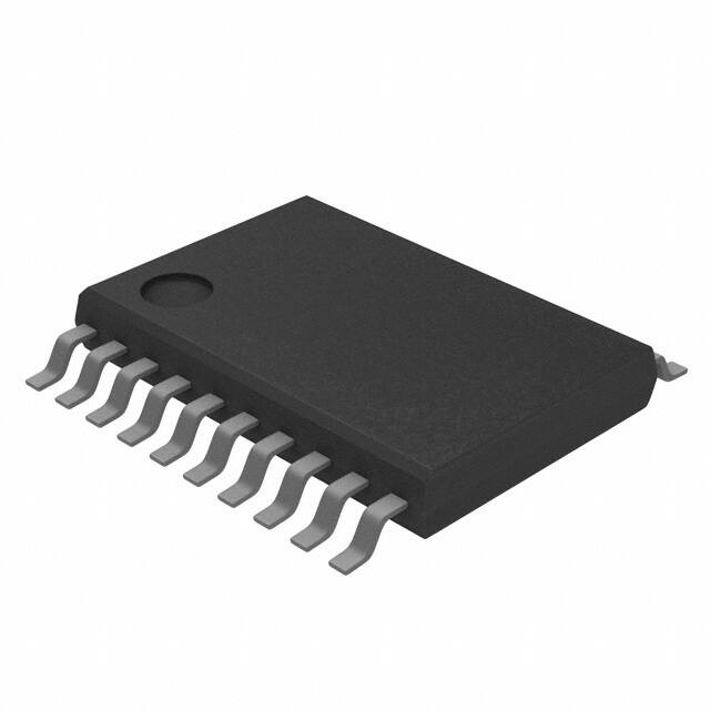
3-channel is built in TSSOP-20P package. Each channel can be controlled and soft-start.
The MB39A112 contains a constant voltage bias circuit for output block, capable of implementing an efficient high-frequency DC/DC
converter. It is ideal for built-in power supply such as ADSL modems.
Features
■
Supports for down-conversion (CH1 to CH3)
■
Power supply voltage range
: 7 V to 25 V
■
Error amplifier threshold voltage
: 1.00 V ± 1% (CH1)
: 1.23 V ± 1% (CH2, CH3)
■
Oscillation frequency range
: 250 kHz to 2.6 MHz
■
Built-in soft-start circuit independent of loads
■
Built-in timer-latch short-circuit protection circuit
■
Built-in totem-pole type output for P-channel MOS FET devices
■
Built-in constant voltage (VCCO - 5 V) bias circuit for output block
Package
20-pin plastic TSSOP
(FPT-20P-M06)
Cypress Semiconductor Corporation
Document Number: 002-08829 Rev. *C
•
198 Champion Court
•
San Jose, CA 95134-1709
•
408-943-2600
Revised January 25, 2019
�MB39A112
Contents
Pin Assignment ................................................................ 3
Pin Description ................................................................. 4
Block Diagram .................................................................. 5
Absolute Maximum Ratings ............................................ 6
Recommended Operating Conditions ............................ 6
Electrical Characteristics ................................................. 7
Typical Characteristics .................................................... 9
Function .......................................................................... 12
DC/DC Converter Function ....................................... 12
Protective Function .................................................... 12
Setting The Output Voltage ........................................... 14
Setting The Triangular Oscillation Frequency............. 14
Setting The Soft-start And Discharge Times ............... 15
Treatment Without Using CS Terminal ......................... 16
Document Number: 002-08829 Rev. *C
Setting Time Constant For Timer-latch
Short-circuit Protection Circuit ..................................... 17
Treatment Without Using CSCP Terminal .................... 18
I/O Equivalent Circuit ..................................................... 19
Application Example ...................................................... 20
Parts List ......................................................................... 21
Selection Of Components .............................................. 22
Reference Data ............................................................... 32
Usage Precaution ........................................................... 35
Ordering Information ...................................................... 35
Package Dimension ....................................................... 36
Document History ........................................................... 37
Sales, Solutions, and Legal Information ...................... 38
Page 2 of 38
�MB39A112
1. Pin Assignment
(TOP VIEW)
CS1 : 1
20 : VCCO
−INE1 : 2
19 : OUT1
FB1 : 3
18 : OUT2
VCC : 4
17 : OUT3
RT : 5
16 : VH
CT : 6
15 : GNDO
GND : 7
14 : CSCP
FB2 : 8
13 : FB3
−INE2 : 9
12 : −INE3
CS2 : 10
11 : CS3
(FPT-20P-M06)
Document Number: 002-08829 Rev. *C
Page 3 of 38
�MB39A112
2. Pin Description
Pin No.
Symbol
I/O
Descriptions
1
CS1
⎯
2
- INE1
I
CH1 error amplifer inverted input terminal.
CH1 soft-start setting capacitor connection terminal.
3
FB1
O
CH1 error amplifer output terminal.
4
VCC
Control circuit power supply terminal.
5
RT
6
CT
7
GND
⎯
⎯
⎯
⎯
8
FB2
O
CH2 error amplifier output terminal.
9
- INE2
I
CH2 error amplifier inverted input terminal.
10
CS2
Triangular-wave oscillation frequency setting resistor connection terminal.
Triangular-wave oscillation frequency setting capacitor connection terminal.
Ground terminal.
11
CS3
⎯
⎯
12
- INE3
I
CH3 error amplifier inverted input terminal.
13
FB3
O
CH3 error amplifier output terminal.
14
CSCP
Timer-latch short-circuit protection capacitor connection terminal.
15
GNDO
⎯
⎯
16
VH
O
Power supply terminal for driving output circuit. (VH = VCCO - 5 V) .
17
OUT3
O
CH3 external Pch MOS FET gate driving terminal.
18
OUT2
O
CH2 external Pch MOS FET gate driving terminal.
19
OUT1
O
CH1 external Pch MOS FET gate driving terminal.
⎯
Power supply terminal for driving output circuit. (Connect to same potential as VCC
terminal).
20
VCCO
Document Number: 002-08829 Rev. *C
CH2 soft-start setting capacitor connection terminal.
CH3 soft-start setting capacitor connection terminal.
Ground terminal.
Page 4 of 38
�MB39A112
3. Block Diagram
Threshold voltage
1.0 V ± 1%
−INE1 2
CH1
VREF
10 μA
−
+
+
CS1 1
L
priority
Error
Amp1
+
20 VCCO
PWM
Comp.1
Drive1
19 OUT1
Pch
−
1.0 V
FB1 3
IO = 150 mA
Threshold voltage
1.23 V ± 1%
−INE2 9
CH2
VREF
10 μA
−
+
+
CS2 10
L
priority
Error
Amp2
+
PWM
Comp.2
Drive2
−
18 OUT2
Pch
1.23 V
FB2 8
IO = 150 mA
Threshold voltage
1.23 V ± 1%
−INE3 12
CH3
VREF
10 μA
−
+
+
CS3 11
L
priority
Error
Amp3
+
PWM
Comp.3
Drive3
17 OUT3
Pch
−
1.23 V
FB3 13
IO = 150 mA
H
priority
SCP
Comp.
VCCO − 5 V
+
+
+
−
16 VH
Bias
Voltage
VH
2.7 V
15 GNDO
SCP
Error Amp Power Supply
SCP Comp. Power Supply
H: at SCP
CSCP 14
2.5 V
4 VCC
H: UVLO
2.0 V
ErrorAmp Reference
1.0 V/1.23 V
bias
3.5 V
OSC
UVLO
VREF
VR
Power
ON/OFF
CTL
GND
5
RT
6
CT
Document Number: 002-08829 Rev. *C
7
GND
Page 5 of 38
�MB39A112
4. Absolute Maximum Ratings
Parameter
Power supply voltage
Symbol
Vcc
Rating
Conditions
VCC, VCCO terminal
Unit
Min
Max
—
28
V
Output current
Io
OUT1, OUT2, OUT3 terminal
—
20
mA
Peak output current
IOP
Duty ≤ 5 % (t = 1/fosc × Duty)
—
400
mA
Power dissipation
PD
—
1280*
mW
- 55
+ 125
°C
Storage temperature
Ta ≤ + 25 °C
TSTG
—
* : The package is mounted on the dual-sided epoxy board (10 cm × 10 cm) .
WARNING:
Semiconductor devices can be permanently damaged by application of stress (voltage, current, temperature, etc.) in
excess of absolute maximum ratings. Do not exceed these ratings.
5. Recommended Operating Conditions
Parameter
Symbol
Conditions
Value
Min
Typ
Max
Unit
Power supply voltage
Vcc
VCC, VCCO terminal
7
12
25
V
Input voltage
VIN
- INE terminal
0
Vcc - 1.8
V
IO
OUT1, OUT2, OUT3 terminal
15
mA
IVH
VH terminal
0
⎯
⎯
⎯
30
mA
250
1200
2600
kHz
22
100
1000
pF
Output current
Oscillation frequency
Timing capacitor
⎯
⎯
⎯
fosc
CT
Timing resistor
RT
VH terminal capacitor
CVH
VH terminal
Soft-start capacitor
CS
Short-circuit detection
capacitor
Operating ambient
temperature
WARNING:
CSCP
Ta
- 15
4.7
10
22
kΩ
0.1
1.0
CS1, CS2, CS3 terminal
⎯
⎯
0.1
1.0
μF
μF
CSCP terminal
⎯
0.01
1.0
μF
- 30
+ 25
+ 85
°C
⎯
The recommended operating conditions are required in order to ensure the normal operation of the semiconductor
device. All of the device’s electrical characteristics are warranted when the device is operated within these ranges.
Always use semiconductor devices within their recommended operating condition ranges. Operation outside these
ranges may adversely affect reliability and could result in device failure.
No warranty is made with respect to uses, operating conditions, or combinations not represented on the data sheet.
Users considering application outside the listed conditions are advised to contact their Cypress representatives
beforehand.
Document Number: 002-08829 Rev. *C
Page 6 of 38
�MB39A112
6. Electrical Characteristics
(VCC = VCCO = 12 V, Ta = + 25 °C)
Parameter
Undervoltage
Lockout
Protection
Circuit Block
[UVLO]
Short-circuit
Protection
Circuit Block
[SCP]
Symbol
Pin No.
Threshold voltage
VTH
4
Hysteresis width
VHYS
4
Threshold voltage
VTH
14
Input source current
ICSCP
14
Reset voltage
VRST
4
fosc
17 to 19
ICS
1, 10, 11
VTH
2
Input bias current
IB
2
- INE1 = 0 V
Voltage gain
AV
3
DC
BW
3
AV = 0dB
VOH
3
Triangular Wave
Oscillation
Oscillator Block
frequency
[OSC]
Soft-start Block
[CS1, CS2,
Charge current
CS3]
Threshold voltage
Error Amp Block Frequency band width
(CH1) [Error
Amp1]
Output voltage
Conditions
Value
Unit
Min
Typ
Max
6.35
6.55
6.75
V
⎯
⎯
0.15
⎯
V
⎯
⎯
0.67
0.72
0.77
V
- 1.4
- 1.0
- 0.6
μA
6.2
6.4
6.6
V
CT = 100 pF,
RT = 10 kΩ
1080
1200
1320
kHz
⎯
- 14
- 10
-6
μA
FB1 = 2.25 V
0.99
1.00
1.01
V
- 250
- 63
100
⎯
1.5*
3.2
3.4
⎯
⎯
⎯
⎯
⎯
⎯
nA
60
40
200
mV
-2
-1
mA
150
250
⎯
μA
1.218
1.230
1.242
V
nA
VCC =
VCC =
⎯
⎯
dB
MHz
V
VOL
3
ISOURCE
3
Output sink current
ISINK
3
Threshold voltage
VTH
9, 12
Input bias current
IB
9, 12
- INE2 = - INE3 = 0 V
- 250
- 63
Voltage gain
AV
8, 13
DC
60
100
BW
8, 13
AV = 0 dB
⎯
1.5*
VOH
8, 13
3.2
3.4
⎯
⎯
⎯
⎯
⎯
⎯
40
200
mV
-2
-1
mA
150
250
⎯
μA
Output source current
Error Amp Block
Frequency band width
(CH2, CH3)
[Error Amp2,
Output voltage
Error Amp3]
Output source current
Output sink current
VOL
8, 13
ISOURCE
8, 13
ISINK
8, 13
FB1 = 2.25 V
FB1 = 2.25 V
FB2 = FB3 = 2.25 V
⎯
⎯
FB2 = FB3 = 2.25 V
FB2 = FB3 = 2.25 V
dB
MHz
V
* : Standard design value
(Continued)
Document Number: 002-08829 Rev. *C
Page 7 of 38
�MB39A112
(Continued)
(VCC = VCCO = 12 V, Ta = + 25 °C)
Parameter
Symbol
Pin No.
Conditions
Value
Unit
Min
Typ
Max
17 to 19 Duty cycle = 0 %
1.9
2.0
⎯
V
17 to 19 Duty cycle = 100 %
⎯
2.5
2.6
V
PWM
Comparator
Block
[PWM Comp.]
Threshold voltage
Bias Voltage
Block [VH]
Output voltage
VH
Output source
current
ISOURCE
Duty ≤ 5 %
17 to 19 OUT1 = OUT2 = OUT3 =
7V
⎯
- 150*
⎯
mA
ISINK
Duty ≤ 5 %
17 to 19 OUT1 = OUT2 = OUT3 =
12 V
⎯
150*
⎯
mA
ROH
17 to 19
OUT1 = OUT2 = OUT3 =
- 15 mA
⎯
13
19.5
Ω
ROL
17 to 19
OUT1 = OUT2 = OUT3 =
15 mA
⎯
10
15
Ω
ICC
4
⎯
⎯
6
9
mA
Output Block
[Drive]
VT0
Output sink current
VT100
16
Output ON resistor
General
Power supply
current
⎯
VCCO - 5.5 VCCO - 5.0 VCCO - 4.5
V
* : Standard design value
Document Number: 002-08829 Rev. *C
Page 8 of 38
�MB39A112
7. Typical Characteristics
Power supply current ICC (mA)
Power Supply Current vs. Power Supply Voltage
10
Ta = +25 °C
RT = OPEN
8
6
4
2
0
0
5
10
15
20
25
Power supply voltage VCC (V)
Error Amp (ERR2, ERR3)
Threshold Voltage vs. Ambient Temperature
2.0
2.0
VCC = 12 V
FB1 = 0 mA
1.5
1.0
0.5
0.0
−0.5
−1.0
−1.5
−2.0
−40 −20
0
20
40
60
80 100
Threshold voltage ΔVTH (%)
Threshold voltage ΔVTH (%)
Error Amp (ERR1)
Threshold Voltage vs. Ambient Temperature
1.0
0.5
0.0
−0.5
−1.0
−1.5
−2.0
−40 −20
CT = 22 pF
CT = 100 pF
CT = 1000 pF CT = 390 pF
100
10
10
100
Timing resistor RT (kΩ)
1000
Triangular wave oscillation frequency
fosc (kHz)
Triangular wave oscillation frequency
fosc (kHz)
Ta = +25 °C
VCC = 12 V
1
20
40
60
80
100
Triangular Wave Oscillation Frequency vs.
Timing Capacitor
Triangular Wave Oscillation Frequency vs.
Timing Resistor
1000
0
Ambient temperature Ta ( °C)
Ambient temperature Ta ( °C)
10000
VCC = 12 V
FB2(3) = 0 mA
1.5
10000
Ta = +25 °C
VCC = 12 V
1000
RT = 4.7 kΩ
RT = 22 kΩ
100
10
10
100
RT = 10 kΩ
1000
10000
Timing capacitor CT (pF)
(Continued)
Document Number: 002-08829 Rev. *C
Page 9 of 38
�MB39A112
2.8
Ta = +25 °C
VCC = 12 V
CT = 100 pF
2.6
Upper
2.4
2.2
Lower limit
2.0
1.8
0
500 1000 1500 2000 2500 3000
Triangular wave oscillation frequency
fosc (kHz)
Triangular Wave Upper/Lower Limit Voltage vs.
Ambient Temperature
Triangular wave upper/lower limit voltage
VCT (V)
Triangular wave upper/lower limit voltage
VCT (V)
Triangular Wave Upper/Lower Limit Voltage vs.
Triangular Wave Oscillation Frequency
1300
1250
1200
1150
1100
1050
1000
−40 −20
0
20
40
60
80
Ambient temperature Ta ( °C)
100
Triangular wave oscillation frequency
fosc (kHz)
Triangular wave oscillation frequency
fosc (kHz)
VCC = 12 V
RT = 10 kΩ
CT = 100 pF
1350
2.6
VCC = 12 V
RT = 10 kΩ
CT = 100 pF
Upper limit
2.4
2.2
Lower limit
2.0
1.8
−40 −20
0
20
40
60
80
100
Ambient temperature Ta ( °C)
Triangular Wave Oscillation Frequency vs.
Power Supply Voltage
Triangular Wave Oscillation Frequency vs.
Ambient Temperature
1400
2.8
1400
Ta = +25 °C
RT = 10 kΩ
CT = 100 pF
1350
1300
1250
1200
1150
1100
1050
1000
0
5
10
15
20
25
30
Power supply voltage VCC (V)
(Continued)
Document Number: 002-08829 Rev. *C
Page 10 of 38
�MB39A112
(Continued)
Error Amp (CH1)
Gain, Phase vs. Frequency
Ta = +25 °C
VCC = 12 V
40
AV
30
240 kΩ
90
10
0
0
−10
−90
−20
Phase ϕ (deg)
ϕ
20
Gain AV (dB)
180
10 kΩ
1 μF
+
IN
2
−
1
+
+
2.4 kΩ
10 kΩ
3.5 V
3
OUT
Error Amp1
1.0 V
−30
−180
−40
100
1k
10 k
100 k
1M
10 M
Frequency f (Hz)
Error Amp (CH2, CH3)
Gain, Phase vs. Frequency
40
AV
30
Ta = +25 °C
VCC = 12 V
240 kΩ
ϕ
10 kΩ
1 μF
+
10
0
0
−10
−90
−20
Phase ϕ (deg)
90
20
Gain AV (dB)
180
IN
2.4 k
10 kΩ
9
(12)
10
(11)
3.5 V
−
+
+
1.23 V
8
OUT
(13)
Error Amp2
(Error Amp3)
−30
−180
−40
100
1k
10 k
100 k
1M
10 M
Frequency f (Hz)
Maximum power dissipation PD (mW)
Maximum Power Dissipation vs. Ambient Temperature
1400
1300
1280
1200
1100
1000
900
800
700
600
500
400
300
200
100
0
−40
Document Number: 002-08829 Rev. *C
−20
0
20
40
60
Ambient temperature Ta ( °C)
80
100
Page 11 of 38
�MB39A112
8. Function
8.1 DC/DC Converter Function
8.1.1 Triangular Wave Oscillator Block (OSC)
The triangular wave oscillator incorporates a timing capacitor and a timing resistor connected respectively to the CT terminl (pin 6)
and RT terminl (pin 5) to generate triangular oscillation waveform amplitude of 2.0 V to 2.5 V. The triangular waveforms are input to
the PWM comparator in the IC.
8.1.2 Error Amplifier Block (Error Amp1, Error Amp2, Error Amp3)
The error amplifier detects the DC/DC converter output voltage and outputs PWM control signals. In addition, an arbitrary loop gain
can be set by connecting a feedback resistor and capacitor from the output terminal to inverted input terminal of the error amplifier,
enabling stable phase compensation to the system.
Also, it is possible to prevent rush current at power supply start-up by connecting a soft-start capacitor with the CS1 terminl (pin 1) ,
CS2 terminl (pin10) and CS3 terminl (pin 11) which are the non-inverted input terminal for Error Amp. The use of error Amp for softstart detection makes it possible for a system to operate on a fixed soft-start time that is independent of the output load on the DC/
DC converter.
8.1.3 PWM Comparator Block (PWM Comp.)
The PWM comparator is a voltage-to-pulse width modulator that controls the output duty depending on the input/output voltage.
The comparator keeps output transistor on while the error amplifier output voltage remain higher than the triangular wave voltage.
8.1.4 Output Block
The output blobk is in the totem pole configulation, capable of driving an external P-channel MOS FET.
8.1.5 Bias Voltage Block (VH)
This bias voltage circuit outputs VCC - 5 V (Typ) as minimum potential of the output circuit.
8.2 Protective Function
8.2.1 Timer Latch Short-circuit Protection Circuit (SCP)
Each channel has a short-circuit detection comparator (SCP Comp.) which constantly compares the error Amp. output level to the
reference voltage.
While DC/DC converter load conditions are stable on all channels, the short-circuit detection comparator output remains at “L”, and
the CSCP terminal is held at “L” level.
If the load condition on a channel changes rapidly due to a short-circuit of the load, causing the output voltage to drop, the output of
the short-circuit detection comparator on that channel goes to “H” level. This causes the external short-circuit protection capacitor
CSCP connected to the CSCP terminal (pin 14) to be charged.
When the capacitor CSCP is charged to the threshold voltage (VTH ≈ 0.72 V) , the latch is set and the external FET is turned off (dead
time is set to 100 %) . At this point, the latch input is closed and the CSCP terminal is held at “L” level.
The latch applied by the timer-latch short-circuit protection circuit can be reset by recycling the power supply (VCC) (See “Setting
Time Constant For Timer-latch Short-circuit Protection Circuit”) .
Document Number: 002-08829 Rev. *C
Page 12 of 38
�MB39A112
8.2.2 Undervoltage Lockout Protection Circuit Block (UVLO)
The transient state or a momentary decrease in supply voltage, which occurs when the power supply is turned on, may cause the IC
to malfunction, resulting in breakdown or degradation of the system. To prevent such malfunctions, under voltage lockout protection
circuit detects a decrease in internal reference voltage with respect to the power supply voltage, turns off the output transistor, and
sets the dead time to 100% while holding the CSCP terminal (pin 14) at the “L” level.
The circuit restores the output transistor to normal when the supply voltage reaches the threshold voltage of the undervoltage lockout
protection circuit.
8.2.3 Protection Circuit Operating Function Table
This table refers to output condition when each protection circuit is operating.
Operating circuit
CH1
CH2
CH3
OUT1
OUT2
OUT3
Short-circuit protection circuit
H
H
H
Under-voltage lockout circuit
H
H
H
The latch can be reset as follows after the short-circuit protection circuit is actuated.
Recycling VCC resets the latch whenever the short-circuit protection circuit has been actuated.
Document Number: 002-08829 Rev. *C
Page 13 of 38
�MB39A112
9. Setting The Output Voltage
• CH1
VO
R1
Error Amp
−
2
−INE1
VO (V) =
+
+
R2
1.00
R2
(R1 + R2)
1.00 V
CS1
1
• CH2, CH3
VO
R1
(−INE3)
12
9
−INE2
Error Amp
−
+
+
R2
VO (V) =
1.23
R2
(R1 + R2)
1.23 V
(CS3)
CS2
11
10
10. Setting The Triangular Oscillation Frequency
The triangular oscillation frequency is determined by the timing capacitor (CT) connected to the CT terminal
(pin 6) and the timing resistor (RT) connected to the RT terminal (pin 5) .
Triangular oscillation frequency : fosc
fosc (kHz) ≈
1200000
CT (pF) • RT (kΩ)
Document Number: 002-08829 Rev. *C
Page 14 of 38
�MB39A112
11. Setting The Soft-start And Discharge Times
To prevent rush currents when the IC is turned on, you can set a soft-start by connecting soft-start capacitors (CS1, CS2 and CS3) to the
CS1 terminal (pin 1) for channel 1, CS2 terminal (pin 10) for channel 2 and CS3 terminal (pin 11) for channel 3 respectively.
Setting each control terminal (CTLX) from “H” to “L” starts charging the external soft-start capacitors (CS1, CS2 and CS3) connected to
the CS1, CS2 and CS3 terminal at about 10 μA. The DC/DC converter output voltage rises in proportion to the CS terminal voltage.
Also, soft-start time is obtained by the following formulas.
Soft-start time : ts (time to output 100%)
CH1
:
CH2
:
CH3
:
ts1[s] ≈ 0.100 × CS1[μF]
ts2[s] ≈ 0.123 × CS2[μF]
ts3[s] ≈ 0.123 × CS3[μF]
• Soft-start circuit
−INE1
(−INE2)
(−INE3)
L
priority
VO
CS1
(CS2)
(CS3)
VREF
10 μA
CH1 ON/OFF signal
−
+
+
Error
Amp
(L : ON, H : OFF)
FB1
(FB2)
(FB3)
CTLX
1.23 V
/1.0 V
H : at SCP
SCP
UVLO
H: UVLO release
• Soft-start operation
CS terminal voltage
≈ 3.4 V
Error Amp. reference voltage
≈ 1.23 V/
1.00 V
≈0V
t
Soft-start time ts
H
CTLX signal
L
t
Document Number: 002-08829 Rev. *C
Page 15 of 38
�MB39A112
12. Treatment Without Using CS Terminal
When not using the soft-start function, open the CS1 terminal (pin 1) , CS2 terminal (pin 10) and CS3 terminal (pin 11) .
• Without setting soft-start tme
“Open”
1 CS1
“Open”
10 CS2
“Open”
11 CS3
Document Number: 002-08829 Rev. *C
Page 16 of 38
�MB39A112
13. Setting Time Constant For Timer-latch Short-circuit Protection Circuit
Each channel uses the short-circuit detection comparator (SCP Comp.) to always compare the error amplifier’s output level to the
reference voltage.
While DC/DC converter load conditions are stable on all channels, the short-circuit detection comparator output remains at “L” level,
and the CSCP terminal (pin 14) is held at “L” level.
If the load condition on a channel changes rapidly due to a short-circuit of the load, causing the output voltage to drop, the output of
the short-circuit detection comparator goes to “H” level. This causes the extemal short-circuit protection capacitor CSCP connected to
the CSCP terminal to be charged at 1 μA.
Short-circuit detection time : tcscp
tcscp[s] ≈ 0.72 × CSCP [μF]
When the capacitor CSCP is charged to the threshold voltage (VTH ≈ 0.72 V) , the latch is set and the external FET is turned off (dead
time is set to 100 %) . At this time, the latch input is closed and the CSCP terminal (pin 14) is held at “L” level.
If any of CH1 to CH3 detects a short circuit, all the channels are stopped.
• Timer-latch short-circuit protection circuit
VO
R1
−INE1
(−INE2)
(−INE3)
VREF
10 μA
R2
−
+
+
CS1
(CS2)
(CS3)
Error
Amp
1.23 V
/1.0 V
FB1
(FB2)
(FB3)
SCP
Comp.
+
+
+
−
[SCP]
2.7 V
1 μA
H: UVLO release
CSCP
14
VCC
S
R
Latch
UVLO
H: at SCP
Document Number: 002-08829 Rev. *C
Page 17 of 38
�MB39A112
14. Treatment Without Using CSCP Terminal
When not using the timer-latch short-circuit protection circuit, connect the CSCP terminal (pin 14) to GND with the shortest distance.
• Treatment without using CSCP terminal
14 CSCP
7 GND
Document Number: 002-08829 Rev. *C
Page 18 of 38
�MB39A112
15. I/O Equivalent Circuit
VCC 4
VCC
VREF
(3.5 V)
VCC
VREF
(3.5 V)
ESD
protection
element
ESD
protection
element
2 kΩ
VREF
(3.5 V)
1.2 V
14 CSCP
ESD
protection
element
GND 7
+
CT 6
−
5 RT
GND
GND
VCC
VCC
VREF
(3.5 V)
VREF
(3.5 V)
CSX
−INE1 2
CS1
1.00 V
3 FB1
GND
GND
VCC
VCC
VREF
(3.5 V)
CSX
1.23 V
FBX
GND
GND
VCC
CT
FBX
VCCO
VCCO 20
OUTX
16 VH
VH
GND
GNDO
GNDO 15
X : Each channel No.
Document Number: 002-08829 Rev. *C
Page 19 of 38
�MB39A112
16. Application Example
R6
R7
2.2 kΩ 18 kΩ
A
−INE1
2
CH1
ON/OFF signal
10 μA
CS1
(L : ON, H : OFF)
C7
0.1
μF
CTL1
C8
0.022 μF
R11 R12
4.7 kΩ 56 kΩ
B
CH2
ON/OFF signal
R9
820 Ω
FB1
−INE2
C
R15 R16
680 Ω 30 kΩ
R17
CH3
10 kΩ
ON/OFF signal
CTL3
C14
0.01 μF
C2
4.7 μF
D1
±
9
R14
820 Ω
FB2
L
priority
L2
Q2
CH2
+
PWM
Comp.2
Drive2
−
18
Pch
C3
2.2 μF
OUT2
D2
C4
4.7 μF
C
Stepdown
1.23 V
8
IO = 150 mA
−INE3
Threshold voltage
1%
1.23 V
12
±
VREF
10 μA
CS3
−
+
+
11
R18
1 kΩ
FB3
L
priority
L3
Q3
CH3
V O3
(5.0 V)
IO3 = 0.15 ∼ 0.3 A
10 μH
Error
Amp3
+
PWM
Comp.3
Drive3
17
Pch
−
C5
2.2 μF
OUT3
D3
C6
4.7 μF
1.23 V
13
H
priority
C16
0.1 μF
IO = 150 mA
VCCO − 5 V
+
+
+
−
16
15
H: at SCP
H: UVLO release
2.0 V
ErrorAmp Reference
1.0 V/1.23 V
bias
3.5 V
OSC
GNDO
Error Amp Power Supply
SCP Comp. Power Supply
14
2.5 V
VH
Bias
Voltage
VH
SCP
CSCP
VO2
(3.3 V)
IO2 = 0.15 ∼ 1 A
3.3 μH
Error
Amp2
−
+
+
10
Stepdown
B
Threshold voltage
1.23 V
1%
2.7 V
C15
1000 pF
C1
2.2 μF
OUT1
1.0 V
SCP
Comp.
Charge
current
1 μA
19
VO1
(1.2 V)
IO1 = 0.8 ∼ 1.5 A
2 μH
3
10 μA
(L : ON, H : OFF)
C13
0.1
μF
Drive1
Pch
L1
Q1
VCCO
C17
0.1 μF
PWM
Comp.1
−
VREF
CS2
C11
0.01 μF
VIN
(12 V)
L
priority
+
20
IO = 150 mA
(L : ON, H : OFF)
CTL2
Error
Amp1
−
+
+
1
R13
36 kΩ
C12
0.1
μF
CH1
VREF
R8
100 kΩ
Stepdown
A
Threshold voltage
1.0 V ± 1 %
UVLO
VREF
VR
4
VCC
C9
0.1 μF
Power
ON/OFF
CTL
GND
5
RT
R10
5.1 kΩ
Document Number: 002-08829 Rev. *C
6
7
CT
GND
C10
100 pF
Page 20 of 38
�MB39A112
17. Parts List
COMPONENT
ITEM
SPECIFICATION
VENDOR
PARTS No.
Q1, Q2,
Q3
Pch FET
Pch FET
VDS = - 30 V, ID = - 2.0 A
VDS = - 30 V, ID = - 1.0 A
SANYO
SANYO
MCH3312
MCH3308
D1, D2
D3
Diode
Diode
SANYO
SANYO
SBE001
SBE005
L1
L2
L3
Inductor
Inductor
Inductor
3 A, 16 mΩ
2.57 A, 21.4 mΩ
1.49 A, 41.2 mΩ
TOKO
TOKO
TOKO
A916CY-2R0M
A916CY-3R3M
A916CY-100M
C1, C3, C5
C2, C4, C6
C7, C9, C12
C8
C10
C11, C14
C13, C16, C17
C15
Ceramics Condenser
Ceramics Condenser
Ceramics Condenser
Ceramics Condenser
Ceramics Condenser
Ceramics Condenser
Ceramics Condenser
Ceramics Condenser
2.2 μF
4.7 μF
0.1 μF
0.022 μF
100 pF
0.01 μF
0.1 μF
1000 pF
25 V
10 V
50 V
50 V
50 V
50 V
50 V
50 V
TDK
TDK
TDK
TDK
TDK
TDK
TDK
TDK
C3216JB1E225K
C3216JB1A475M
C1608JB1H104K
C1608JB1H223K
C1608CH1H101J
C1608JB1H103K
C1608JB1H104K
C1608JB1H102K
R6
R7
R8
R9
R10
R11
R12
R13
R14
R15
R16
R17
R18
Resistor
Resistor
Resistor
Resistor
Resistor
Resistor
Resistor
Resistor
Resistor
Resistor
Resistor
Resistor
Resistor
2.2 kΩ
18 kΩ
100 kΩ
820 Ω
5.1 kΩ
4.7 kΩ
56 kΩ
36 kΩ
820 Ω
680 Ω
30 kΩ
10 kΩ
1 kΩ
0.5 %
0.5 %
0.5 %
0.5 %
0.5 %
0.5 %
0.5 %
0.5 %
0.5 %
0.5 %
0.5 %
0.5 %
0.5 %
ssm
ssm
ssm
ssm
ssm
ssm
ssm
ssm
ssm
ssm
ssm
ssm
ssm
RR0816P-222-D
RR0816P-183-D
RR0816P-104-D
RR0816P-821-D
RR0816P-512-D
RR0816P-472-D
RR0816P-563-D
RR0816P-363-D
RR0816P-821-D
RR0816P-681-D
RR0816P-303-D
RR0816P-103-D
RR0816P-102-D
VF = 0.55 V (Max) , at IF = 2 A
VF = 0.4 V (Max) , at IF = 0.5 A
2 μH
3.3 μH
10 μH
Note :
SANYO
: SANYO Electric Co., Ltd.
TOKO
: TOKO Inc.
TDK
: TDK Corporation
ssm
: SUSUMU Co., Ltd.
Document Number: 002-08829 Rev. *C
Page 21 of 38
�MB39A112
18. Selection Of Components
■
Pch MOS FET
The Pch MOS FET for switching use should be rated for at least 20 % or more than the maximum input voltage. To minimize continuity
loss, use a FET with low RDS (ON) between the drain and source. For high input voltage and high frequency operation, on-cycle
switching loss will be higher so that power dissipation must be considered. In this application, the SANYO MCH3312 and MCH3308
are used. Continuity loss, on/off-cycle switching loss and total loss are determined by the following formulas. The selection must
ensure that peak drain current does not exceed rated values.
Continuity loss : Pc
PC =
ID2 × RDS (ON) × Duty
On-cycle switching loss : PS (ON)
PS (ON)
VD (Max) × ID × tr × fosc
=
6
Off-cycle switching loss : PS (OFF)
PS (OFF)
VD (Max) × ID (Max) × tf × fosc
=
6
Total loss : PT
PT =
PC + PS (ON) + PS (OFF)
Example : Using the MCH3312
■
CH1
Input voltage VIN = 12 V, output voltage VO = 1.2 V, drain current ID = 1.5 A, oscillation frequency fOSC = 2350 kHz, L = 2 μH, drainsource on resistance RDS(ON) ≈ 180 mΩ, tr ≈ 2.9 ns, tf ≈ 8.7 ns.
Drain current (Max) : ID (Max)
ID (Max) =
Io +
=
1.5 +
≈
VIN - Vo
2L
tON
12 - 1.2
2 × 2.0 × 10 -6
×
1
2350 × 103
×
0.1
×
0.1
1.61 A
Drain current (Min) : ID (Min)
ID (Min) =
=
≈
Io -
1.5 -
VIN - Vo
2L
tON
12 - 1.2
2 × 2.0 × 10
-6
×
1
2350 × 103
1.39 A
Document Number: 002-08829 Rev. *C
Page 22 of 38
�MB39A112
PC = ID2 × RDS (ON) × Duty
=
1.52 × 0.18 × 0.1
≈ 0.04 W
PS (ON)
PS (OFF)
=
VD × ID × tr × fosc
=
12 × 1.5 × 2.9 × 10 -9 × 2350 × 103
≈
0.02 W
=
=
≈
6
6
VD × ID (Max) × tf × fosc
6
12 × 1.61 × 8.7 × 10 -9 × 2350 × 103
6
0.066 W
PT =
PC + PS (ON) + PS (OFF)
≈
0.04 + 0.02 + 0.066
≈ 0.126 W
The above power dissipation figures for the MCH3312 are satisfied with ample margin at 1.0 W Ta = +25°C
e
(
■
)
CH2
Input voltage VIN = 12 V, output voltage VO = 3.3 V, drain current ID = 1.0 A, oscillation frequency fOSC = 2350 kHz, L = 3.3 μH, drainsource on resistance RDS(ON) ≈ 180 mΩ, tr ≈ 2.9 ns, tf ≈ 8.7 ns.
Drain current (Max) : ID (Max)
ID (Max) =
Io +
=
1 +
≈
1.15 A
VIN - Vo
2L
tON
12 - 3.3
2 × 3.3 × 10
-6
×
1
2350 × 103
×
0.275
×
0.275
Drain current (Min) : ID (Min)
ID (Min) =
Io -
=
1 -
≈
0.85 A
VIN - Vo
2L
tON
12 - 3.3
2 × 3.3 × 10
−6
Document Number: 002-08829 Rev. *C
×
1
2350 × 103
Page 23 of 38
�MB39A112
PC = ID2 × RDS (ON) × Duty
=
12 × 0.18 × 0.275
≈ 0.0495 W
PS (ON) =
=
≈
PS (OFF) =
PT =
VD × ID × tr × fosc
6
12 × 1 × 2.9 × 10 -9 × 2350 × 103
6
0.0136 W
VD × ID (Max) × tf × fosc
6
=
12 × 1.15 × 8.7 × 10 -9 × 2350 × 103
≈
0.047 W
6
PC + PS (ON) + PS (OFF)
≈
0.0495 + 0.0136 + 0.047
≈
0.11 W
The above power dissipation figures for the MCH3312 are satisfied with ample margin at 1.0 W (Ta = +25°C) .
Example : Using the MCH3308
■
CH3
Input voltage VIN = 12 V, output voltage Vo = 5.0 V, drain current ID = 0.3 A, oscillation frequency fosc =
2350 kHz, L = 10 μH, drain-source on resistance RDS (ON) ≈ 600 mΩ, tr ≈ 4 ns, tf ≈ 4 ns.
Drain current (Max) : ID (Max)
ID (Max) =
Io +
=
0.3 +
≈
VIN - Vo
2L
tON
12 - 5
2 × 10 × 10
-6
×
1
2350 × 103
×
0.417
0.36 (A)
Document Number: 002-08829 Rev. *C
Page 24 of 38
�MB39A112
Drain current (Min) : ID (Min)
VIN - Vo
ID (Min) =
Io -
=
0.3 -
≈
0.24 (A)
tON
2L
12 - 5
2 × 10 × 10
-6
×
1
2350 × 103
×
0.417
PC = ID2 × RDS (ON) × Duty
=
0.32 × 0.6 × 0.417
≈ 0.023 W
PS (ON) =
=
≈
PS (OFF) =
PT =
VD × ID × tr × fosc
6
12 × 0.3 × 4 × 10 -9 × 2350 × 103
6
0.0056 W
VD × ID (Max) × tf × fosc
6
=
12 × 0.36 × 4 × 10 -9 × 2350 × 103
≈
0.0068 W
6
PC + PS (ON) + PS (OFF)
≈
0.023 + 0.0056 + 0.0068
≈
0.0354 W
The above power dissipation figures for the MCH3308 are satisfied with ample margin at 0.8 W (Ta = +25°C) .
Document Number: 002-08829 Rev. *C
Page 25 of 38
�MB39A112
■
Inductors
In selecting inductors, it is of course essential not to apply more current than the rated capacity of the inductor, but also to note that
the lower limit for ripple current is a critical point that if reached will cause discontinuous operation and a considerable drop in efficiency.
This can be prevented by choosing a higher inductance value, which will enable continuous operation under light loads. Note that if
the inductance value is too high, however, direct current resistance (DCR) is increased and this will also reduce efficiency. The
inductance must be set at the point where efficiency is greatest.
Note also that the DC superimposition characteristics become worse as the load current value approaches the rated current value of
the inductor, so that the inductance value is reduced and ripple current increases, causing loss of efficiency. The selection of rated
current value and inductance value will vary depending on where the point of peak efficiency lies with respect to load current.
Inductance values are determined by the following formulas.
The L value for all load current conditions is set so that the peak to peak value of the ripple current is 1/2 the load current or less.
Inductance value : L
2 (VIN - Vo)
L≥
Io
tON
Example
■
CH1
L≥
≥
≥
■
Io
2 × (12 -1.2)
1.5
tON
×
1
2350 × 103
×
0.1
×
0.275
×
0.417
0.61 μH
CH2
L≥
≥
≥
■
2 (VIN - Vo1)
2 (VIN - Vo2)
Io
2 × (12 -3.3)
1
tON
×
1
2350 × 103
2.04 μH
CH3
L≥
≥
≥
2 (VIN - Vo3)
Io
2 × (12 - 5)
0.3
tON
×
1
2350 × 103
8.28 μH
Inductance values derived from the above formulas are values that provide sufficient margin for continuous operation at maximum
load current, but at which continuous operation is not possible at light loads. It is therefore necessary to determine the load level at
which continuous operation becomes possible. In this application, the TOKO A916CY-2R0M, A916CY-3R3M and A916CY-100M are
used. At 2 μH, 3.3 μH and 10 μH, the load current value under continuous operating conditions is determined by the following formula.
Document Number: 002-08829 Rev. *C
Page 26 of 38
�MB39A112
Load current value under continuous operating conditions : Io
Io ≥
Vo
tOFF
2L
Example : Using the A916CY-2R0M
2 μH (allowable tolerance ± 20 %), rated current = 3 A
■
CH1
Io ≥
≥
≥
Vo1
tOFF
2L
1.2
2 × 2 × 10
1
×
-6
2350 × 103
×
(1 - 0.1)
0.11 A
Example : Using the A916CY-3R3M
3.3 μH (allowable tolerance ± 20 %) , rated current = 2.57 A
■
CH2
Io ≥
≥
≥
Vo2
tOFF
2L
3.3
2 × 3.3 × 10
-6
×
1
2350 × 103
×
(1 - 0.275)
0.15 A
Example : Using the A916CY-100M
10.0 μH (allowable tolerance ± 20 %) , rated current = 1.49 A
■
CH3
Io ≥
≥
≥
Vo3
2L
tOFF
5
2 × 10 × 10 -6
×
1
2350 × 103
×
(1 - 0.417)
62.0 mA
To determine whether the current through the inductor is within rated values, it is necessary to determine the peak value of the ripple
current as well as the peak-to-peak values of the ripple current that affect the output ripple voltage. The peak value and peak-to-peak
value of the ripple current can be determined by the following formulas.
Document Number: 002-08829 Rev. *C
Page 27 of 38
�MB39A112
Peak value : IL
IL ≥
VIN - Vo
Io +
tON
2L
Peak-to-peak value : ΔIL
VIN - Vo
ΔIL =
tON
L
Example : Using the A916CY-2R0M
2.0 μH (allowable tolerance ± 20 %) , rated current = 3.0 A
CH1
Peak value
■
IL ≥
≥
≥
VIN - Vo1
Io +
2L
1.5 +
tON
12 - 1.2
×
2 × 2.0 × 10 -6
1
2350 × 103
× 0.1
1.61 A
Peak-to-peak value
ΔIL =
=
≈
VIN - Vo1
L
12 - 1.2
2.0 × 10 -6
tON
×
1
2350 × 103
× 0.1
0.23 A
Document Number: 002-08829 Rev. *C
Page 28 of 38
�MB39A112
Example : Using the A916CY-3R3M
3.3 μH (allowable tolerance ± 20 %) , rated current = 2.57 A
CH2
Peak value
■
IL ≥
≥
≥
VIN - Vo2
Io +
tON
2L
12 - 3.3
1.0 +
2 × 3.3 × 10
×
-6
1
2350 × 103
× 0.275
1.15 A
Peak-to-peak value
ΔIL =
VIN - Vo2
=
12 - 3.3
≈
tON
L
3.3 × 10
×
-6
1
2350 × 103
× 0.275
0.309 A
Example : Using the A916CY-100M
10.0 μH (allowable tolerance ± 20 %) , rated current = 1.49 A
CH3
Peak value
■
IL ≥
≥
≥
VIN - Vo3
Io +
tON
2L
0.3 +
12 - 5
2 × 10 × 10
×
-6
1
2350 × 103
× 0.417
0.36 A
Peak-to-peak value
ΔIL =
=
≈
VIN - Vo3
L
12 - 5
10 × 10
-6
tON
×
1
2350 × 103
× 0.417
0.124 A
Document Number: 002-08829 Rev. *C
Page 29 of 38
�MB39A112
■
Flyback diode
The flyback diode is generally used as a Shottky barrier diode (SBD) when the reverse voltage to the diode is less than 40 V. The
SBD has the characteristics of higher speed in terms of faster reverse recovery time, and lower forward voltage, and is ideal for
archiving high efficiency. As long as the DC reverse voltage is sufficiently higher than the input voltage, the average current flowing
through the diode is within the average output current level, and peak current is within peak surge current limits, there is no problem.
In this application the SANYO SBE001, SBS005 are used. The diode average current and diode peak current can be calculated by
the following formulas.
Diode mean current : IDi
IDi ≥
( 1 -
Io ×
Vo
)
VIN
Diode peak current : IDip
IDip ≥
Vo
(Io +
2L
tOFF)
Example : Using the SBE001
VR (DC reverse voltage) = 30 V, average output current = 2.0 A, peak surge current = 20 A,
VF (forward voltage) = 0.55 V, at IF = 2.0 A
CH1
Diode mean current
■
IDi ≥
≥ 1.5
≥
(1 -
Io ×
×
Vo1
VIN
)
(1 - 0.1)
1.35 A
Diode peak current
IDip ≥
≥
Vo1
(Io +
2L
tOFF)
1.61 A
CH2
Diode mean current
■
IDi ≥
Io ×
(1 -
Vo2
VIN
)
≥ 1.0 × (1 - 0.275)
≥
0.725 A
Document Number: 002-08829 Rev. *C
Page 30 of 38
�MB39A112
Diode peak current
IDip ≥
≥
Vo2
(Io +
2L
tOFF)
1.15 A
Example : Using the SBS005
VR (DC reverse voltage) = 30 V, average output current = 1.0 A, peak surge current = 10 A,
VF (forward voltage) = 0.4 V, at IF = 0.5 A
CH3
Diode mean current
■
IDi ≥
≥ 0.3
≥
(1 -
Io ×
×
Vo3
VIN
)
(1 - 0.417)
0.175 A
Diode peak current
IDip ≥
≥
(Io +
Vo3
2L
tOFF)
0.36 A
Document Number: 002-08829 Rev. *C
Page 31 of 38
�MB39A112
19. Reference Data
Conversion Efficiency vs. Load Current Characteristics (CH1)
Ta = + 25 °C
1.2 V output
CTL1 = “L”
CTL2 = “H”
CTL3 = “H”
RT = 5.1 kΩ
CT = 100 pF
Conversion efficiency η (%)
100
90
80
70
VIN = 7 V
VIN = 10 V
VIN = 12 V
60
50
40
30
10 m
100 m
1
10
Load current IL (A)
Conversion Efficiency vs. Load Current Characteristics (CH2)
Ta = + 25 °C
3.3 V output
CTL1 = “H”
CTL2 = “L”
CTL3 = “H”
RT = 5.1 kΩ
CT = 100 pF
Conversion efficiency η (%)
100
90
80
70
VIN = 7 V
VIN = 10 V
VIN = 12 V
60
50
40
30
10 m
100 m
1
10
Load current IL (A)
Conversion Efficiency vs. Load Current Characteristics (CH3)
Ta = + 25 °C
5.0 V output
CTL1 = “H”
CTL2 = “H”
CTL3 = “L”
RT = 5.1 kΩ
CT = 100 pF
100
Conversion efficiency η (%)
90
80
70
60
VIN = 7 V
VIN = 10 V
VIN = 12 V
50
40
30
10 m
100 m
1
10
Load current IL (A)
(Continued)
Document Number: 002-08829 Rev. *C
Page 32 of 38
�MB39A112
Conversion Efficiency vs. Load Current Characteristics (CH1)
=
Conversion efficiency η (%)
100
Ta
+ 25 °C
1.2 V output
CTL1 “L”
CTL2 “H”
CTL3 “H”
RT 10 kΩ
CT 100 pF
90
80
=
=
70
=
=
=
VIN = 7 V
VIN = 10 V
VIN = 12 V
60
50
40
30
10 m
100 m
1
10
Load current IL (A)
Conversion Efficiency vs. Load Current Characteristics (CH2)
Conversion efficiency η (%)
100
Ta = + 25 °C
3.3 V output
CTL1 = “H”
CTL2 = “L”
CTL3 = “H”
RT = 10 kΩ
CT = 100 pF
90
80
70
VIN = 7 V
VIN = 10 V
VIN = 12 V
60
50
40
30
10 m
100 m
1
10
Load current IL (A)
Conversion Efficiency vs. Load Current Characteristics (CH3)
Ta = + 25 °C
5.0 V output
CTL1 = “H”
CTL2 = “H”
CTL3 = “L”
RT = 10 kΩ
CT = 100 pF
Conversion efficiency η (%)
100
90
80
70
60
VIN = 7 V
VIN = 10 V
VIN = 12 V
50
40
30
10m
100m
1
10
Load current IL (A)
(Continued)
Document Number: 002-08829 Rev. *C
Page 33 of 38
�MB39A112
(Continued)
Conversion Efficiency vs. Load Current Characteristics (CH1)
Ta = + 25 °C
1.2 V output
CTL1 = “L”
CTL2 = “H”
CTL3 = “H”
RT = 24 kΩ
CT = 100 pF
Conversion efficiency η (%)
100
90
80
70
60
VIN = 7 V
VIN = 10 V
VIN = 12 V
50
40
30
10 m
100 m
1
10
Load current IL (A)
Conversion Efficiency vs. Load Current Characteristics (CH2)
Ta = + 25 °C
3.3 V output
CTL1 = “H”
CTL2 = “L”
CTL3 = “H”
RT = 24 kΩ
CT = 100 pF
Conversion efficiency η (%)
100
90
80
70
VIN = 7 V
VIN = 10 V
VIN = 12 V
60
50
40
30
10 m
100 m
1
10
Load current IL (A)
Cconversion Efficiency vs. Load Current Characteristics (CH3)
Ta = + 25 °C
5.0 V output
CTL1 = “H”
CTL2 = “H”
CTL3 = “L”
RT = 24 kΩ
CT = 100 pF
Cconversion efficiency η (%)
100
90
80
70
VIN = 7 V
VIN = 10 V
VIN = 12 V
60
50
40
30
10m
100m
1
10
Load current IL (A)
Document Number: 002-08829 Rev. *C
Page 34 of 38
�MB39A112
20. Usage Precaution
■
Printed circuit board ground lines should be set up with consideration for common impedance.
■
Take appropriate static electricity measures.
❐ Containers for semiconductor materials should have anti-static protection or be made of conductive material.
❐ After mounting, printed circuit boards should be stored and shipped in conductive bags or containers.
❐ Work platforms, tools and instruments should be properly grounded.
❐ Working personnel should be grounded with resistance of 250 kΩ to 1 MΩ between body and ground.
■
Do not apply negative voltages.
❐ The use of negative voltages below -0.3 V may create parasitic transistors on LSI lines, which can cause abnormal operation.
21. Ordering Information
Part number
MB39A112PFT
Document Number: 002-08829 Rev. *C
Package
Remarks
20-pin plastic TSSOP
(FPT-20P-M06)
Page 35 of 38
�MB39A112
22. Package Dimension
Note 1)
Note 2)
Note 3)
Note 4)
20-pin plastic TSSOP
(FPT-20P-M06)
*1 : Resin protrusion. (Each side : +0.15 (.006) Max) .
*2 : These dimensions do not include resin protrusion.
Pins width and pins thickness include plating thickness.
Pins width do not include tie bar cutting remainder.
*1 6.50±0.10(.256±.004)
0.17±0.05
(.007±.002)
20
11
*2 4.40±0.10 6.40±0.20
(.173±.004) (.252±.008)
INDEX
Details of "A" part
1.05±0.05
(Mounting height)
(.041±.002)
LEAD No.
1
10
"A"
0.65(.026)
0.24±0.08
(.009±.003)
0.13(.005)
M
0~8˚
+0.03
(0.50(.020))
0.10(.004)
C
0.60±0.15
(.024±.006)
+.001
0.07 –0.07 .003 –.003
(Stand off)
0.25(.010)
2003 FUJITSU LIMITED F20026S-c-3-3
Dimensions in mm (inches) .
Note : The values in parentheses are reference values.
Document Number: 002-08829 Rev. *C
Page 36 of 38
�MB39A112
Document History
Document Title: MB39A112 3-ch DC/DC Converter IC
Document Number: 002-08829
Revision
ECN
Orig. of
Change
Submission
Date
**
—
TAOA
11/25/2003
*A
5491406
TAOA
10/24/2016
Updated to Cypress template.
*B
5904432
MASG
10/02/2017
Adapted Cypress new logo.
*C
6459753
SSAS
01/25/2019
Obsoleted.
Document Number: 002-08829 Rev. *C
Description of Change
Migrated to Cypress and assigned document number 002-08829.
No change to document contents or format.
Page 37 of 38
�MB39A112
Sales, Solutions, and Legal Information
Worldwide Sales and Design Support
Cypress maintains a worldwide network of offices, solution centers, manufacturer’s representatives, and distributors. To find the office
closest to you, visit us at Cypress Locations.
Products
PSoC® Solutions
ARM® Cortex® Microcontrollers
Automotive
cypress.com/arm
cypress.com/automotive
Clocks & Buffers
Interface
Internet of Things
Memory
cypress.com/clocks
cypress.com/interface
cypress.com/iot
cypress.com/memory
Microcontrollers
cypress.com/mcu
PSoC
cypress.com/psoc
Power Management ICs
Touch Sensing
USB Controllers
Wireless/RF
PSoC 1 | PSoC 3 | PSoC 4 | PSoC 5LP | PSoC 6
Cypress Developer Community
Forums | WICED IOT Forums | Projects | Video | Blogs | Training
| Components
Technical Support
cypress.com/support
cypress.com/pmic
cypress.com/touch
cypress.com/usb
cypress.com/wireless
© Cypress Semiconductor Corporation, 2003-2019. This document is the property of Cypress Semiconductor Corporation and its subsidiaries, including Spansion LLC ("Cypress"). This document,
including any software or firmware included or referenced in this document ("Software"), is owned by Cypress under the intellectual property laws and treaties of the United States and other countries
worldwide. Cypress reserves all rights under such laws and treaties and does not, except as specifically stated in this paragraph, grant any license under its patents, copyrights, trademarks, or other
intellectual property rights. If the Software is not accompanied by a license agreement and you do not otherwise have a written agreement with Cypress governing the use of the Software, then Cypress
hereby grants you a personal, non-exclusive, nontransferable license (without the right to sublicense) (1) under its copyright rights in the Software (a) for Software provided in source code form, to
modify and reproduce the Software solely for use with Cypress hardware products, only internally within your organization, and (b) to distribute the Software in binary code form externally to end users
(either directly or indirectly through resellers and distributors), solely for use on Cypress hardware product units, and (2) under those claims of Cypress's patents that are infringed by the Software (as
provided by Cypress, unmodified) to make, use, distribute, and import the Software solely for use with Cypress hardware products. Any other use, reproduction, modification, translation, or compilation
of the Software is prohibited.
TO THE EXTENT PERMITTED BY APPLICABLE LAW, CYPRESS MAKES NO WARRANTY OF ANY KIND, EXPRESS OR IMPLIED, WITH REGARD TO THIS DOCUMENT OR ANY SOFTWARE
OR ACCOMPANYING HARDWARE, INCLUDING, BUT NOT LIMITED TO, THE IMPLIED WARRANTIES OF MERCHANTABILITY AND FITNESS FOR A PARTICULAR PURPOSE. No computing
device can be absolutely secure. Therefore, despite security measures implemented in Cypress hardware or software products, Cypress does not assume any liability arising out of any security breach,
such as unauthorized access to or use of a Cypress product. In addition, the products described in these materials may contain design defects or errors known as errata which may cause the product
to deviate from published specifications. To the extent permitted by applicable law, Cypress reserves the right to make changes to this document without further notice. Cypress does not assume any
liability arising out of the application or use of any product or circuit described in this document. Any information provided in this document, including any sample design information or programming
code, is provided only for reference purposes. It is the responsibility of the user of this document to properly design, program, and test the functionality and safety of any application made of this
information and any resulting product. Cypress products are not designed, intended, or authorized for use as critical components in systems designed or intended for the operation of weapons, weapons
systems, nuclear installations, life-support devices or systems, other medical devices or systems (including resuscitation equipment and surgical implants), pollution control or hazardous substances
management, or other uses where the failure of the device or system could cause personal injury, death, or property damage ("Unintended Uses"). A critical component is any component of a device
or system whose failure to perform can be reasonably expected to cause the failure of the device or system, or to affect its safety or effectiveness. Cypress is not liable, in whole or in part, and you
shall and hereby do release Cypress from any claim, damage, or other liability arising from or related to all Unintended Uses of Cypress products. You shall indemnify and hold Cypress harmless from
and against all claims, costs, damages, and other liabilities, including claims for personal injury or death, arising from or related to any Unintended Uses of Cypress products.
Cypress, the Cypress logo, Spansion, the Spansion logo, and combinations thereof, WICED, PSoC, CapSense, EZ-USB, F-RAM, and Traveo are trademarks or registered trademarks of Cypress in
the United States and other countries. For a more complete list of Cypress trademarks, visit cypress.com. Other names and brands may be claimed as property of their respective owners.
Document Number: 002-08829 Rev. *C
Revised January 25, 2019
Page 38 of 38
�


 工商网监
湘ICP备2023018690号
工商网监
湘ICP备2023018690号
