Click here to ask about the production status of specific part numbers.
MAX40108
1V, Low-Power, Precision Operational Amplifier
General Description
Benefits and Features
The MAX40108 is a low-power, high-precision operational
amplifier (op amp) that operates with a power supply voltage as low as 0.9V.
●
●
●
●
●
●
●
●
●
Available in a space-saving, 1.22mmx 0.92mm, 6-bump
wafer-level package (WLP) with a 0.4mm bump pitch, it is
designed for use in portable, consumer, medical, and industrial applications.
The MAX40108 features rail-to-rail CMOS inputs and outputs, a 168kHz GBW consuming only 25.5µA (typ) supply
current and 1µV (typ) zero-drift input offset voltage over
time and temperature. The zero-drift feature reduces the
high 1/f noise typically found in CMOS input operational
amplifiers, making it useful for a wide variety of low-frequency measurement applications.
The MAX40108 operates from a 0.9V to 3.6V power supply voltage and is specified over the -40°C to +125°C extended operating temperature range.
Applications
● Wearable Devices
● Home Medical (Blood Glucose,Weight Scale, Blood
Pressure, EKG)
● Fitness and Health (Smart Watch, Heart-Rate Monitor)
● Industrial IOT (Pressure, Flow, Level, Temperature,
Proximity)
Typical Application Circuit
19-100763; Rev 0; 7/20
Supply Voltage Range: 0.9V to 3.6V
Low 25.5μA Quiescent Current
Very Low 1μV (typ) Input Offset Voltage
Rail-to-Rail Inputs and Outputs
Internal EMI Rejection
168kHz GBW
Low Input Bias Current
Power-Saving Shutdown Mode
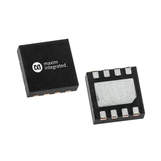
Available in Tiny, 1.22mm x 0.92mm, 6-bump WLP
and 8-pin TDFN
Ordering Information appears at end of data sheet.
�MAX40108
1V, Low-Power, Precision Operational Amplifier
TABLE OF CONTENTS
General Description. . . . . . . . . . . . . . . . . . . . . . . . . . . . . . . . . . . . . . . . . . . . . . . . . . . . . . . . . . . . . . . . . . . . . . . . . . . . . . 1
Applications . . . . . . . . . . . . . . . . . . . . . . . . . . . . . . . . . . . . . . . . . . . . . . . . . . . . . . . . . . . . . . . . . . . . . . . . . . . . . . . . . . . . 1
Benefits and Features . . . . . . . . . . . . . . . . . . . . . . . . . . . . . . . . . . . . . . . . . . . . . . . . . . . . . . . . . . . . . . . . . . . . . . . . . . . . 1
Typical Application Circuit . . . . . . . . . . . . . . . . . . . . . . . . . . . . . . . . . . . . . . . . . . . . . . . . . . . . . . . . . . . . . . . . . . . . . . . . . 1
Absolute Maximum Ratings. . . . . . . . . . . . . . . . . . . . . . . . . . . . . . . . . . . . . . . . . . . . . . . . . . . . . . . . . . . . . . . . . . . . . . . . 3
Package Information . . . . . . . . . . . . . . . . . . . . . . . . . . . . . . . . . . . . . . . . . . . . . . . . . . . . . . . . . . . . . . . . . . . . . . . . . . . . . 3
WLP . . . . . . . . . . . . . . . . . . . . . . . . . . . . . . . . . . . . . . . . . . . . . . . . . . . . . . . . . . . . . . . . . . . . . . . . . . . . . . . . . . . . . . . 3
TDFN . . . . . . . . . . . . . . . . . . . . . . . . . . . . . . . . . . . . . . . . . . . . . . . . . . . . . . . . . . . . . . . . . . . . . . . . . . . . . . . . . . . . . . 3
Electrical Characteristics . . . . . . . . . . . . . . . . . . . . . . . . . . . . . . . . . . . . . . . . . . . . . . . . . . . . . . . . . . . . . . . . . . . . . . . . . 3
Typical Operating Characteristics . . . . . . . . . . . . . . . . . . . . . . . . . . . . . . . . . . . . . . . . . . . . . . . . . . . . . . . . . . . . . . . . . . 6
Pin Configurations . . . . . . . . . . . . . . . . . . . . . . . . . . . . . . . . . . . . . . . . . . . . . . . . . . . . . . . . . . . . . . . . . . . . . . . . . . . . . . . 9
WLP . . . . . . . . . . . . . . . . . . . . . . . . . . . . . . . . . . . . . . . . . . . . . . . . . . . . . . . . . . . . . . . . . . . . . . . . . . . . . . . . . . . . . . . 9
TDFN . . . . . . . . . . . . . . . . . . . . . . . . . . . . . . . . . . . . . . . . . . . . . . . . . . . . . . . . . . . . . . . . . . . . . . . . . . . . . . . . . . . . . . 9
Pin Description . . . . . . . . . . . . . . . . . . . . . . . . . . . . . . . . . . . . . . . . . . . . . . . . . . . . . . . . . . . . . . . . . . . . . . . . . . . . . . . . . 9
Detailed Description . . . . . . . . . . . . . . . . . . . . . . . . . . . . . . . . . . . . . . . . . . . . . . . . . . . . . . . . . . . . . . . . . . . . . . . . . . . . 11
Auto-Zero . . . . . . . . . . . . . . . . . . . . . . . . . . . . . . . . . . . . . . . . . . . . . . . . . . . . . . . . . . . . . . . . . . . . . . . . . . . . . . . . . . 11
Shutdown Operation. . . . . . . . . . . . . . . . . . . . . . . . . . . . . . . . . . . . . . . . . . . . . . . . . . . . . . . . . . . . . . . . . . . . . . . . . . 11
Applications Information . . . . . . . . . . . . . . . . . . . . . . . . . . . . . . . . . . . . . . . . . . . . . . . . . . . . . . . . . . . . . . . . . . . . . . . . . 12
Overview . . . . . . . . . . . . . . . . . . . . . . . . . . . . . . . . . . . . . . . . . . . . . . . . . . . . . . . . . . . . . . . . . . . . . . . . . . . . . . . . . . 12
Power-Up Settling Time . . . . . . . . . . . . . . . . . . . . . . . . . . . . . . . . . . . . . . . . . . . . . . . . . . . . . . . . . . . . . . . . . . . . . . . 12
Capacitive-Load Stability . . . . . . . . . . . . . . . . . . . . . . . . . . . . . . . . . . . . . . . . . . . . . . . . . . . . . . . . . . . . . . . . . . . . . . 12
Power Supplies and Layout . . . . . . . . . . . . . . . . . . . . . . . . . . . . . . . . . . . . . . . . . . . . . . . . . . . . . . . . . . . . . . . . . . . . 12
Ordering Information . . . . . . . . . . . . . . . . . . . . . . . . . . . . . . . . . . . . . . . . . . . . . . . . . . . . . . . . . . . . . . . . . . . . . . . . . . . . 12
Revision History . . . . . . . . . . . . . . . . . . . . . . . . . . . . . . . . . . . . . . . . . . . . . . . . . . . . . . . . . . . . . . . . . . . . . . . . . . . . . . . 13
www.maximintegrated.com
19-100763
Maxim Integrated | 2
�MAX40108
1V, Low-Power, Precision Operational Amplifier
Absolute Maximum Ratings
VDD to GND.............................................................. -0.3V to +4V
IN+ to IN- ...................................................... -0.3V to VDD + 0.3V
OUT to GND ................................................. -0.3V to VDD + 0.3V
IN+, IN- to GND ........................................... -0.3V to VDD + 0.3V
Continuous Current into Any Input/Output Pin .................... 10mA
Output Short-Circuit Duration to Either VDD or GND ..Continuous
Continuous Power Dissipation (Derate 10.51mW/°C above
+70°C)..........................................................................840.78mW
Operating Temperature Range ...........................-40°C to +125°C
Junction Temperature ....................................................... +150°C
Stresses beyond those listed under “Absolute Maximum Ratings” may cause permanent damage to the device. These are stress ratings only, and functional operation of the
device at these or any other conditions beyond those indicated in the operational sections of the specifications is not implied. Exposure to absolute maximum rating conditions for
extended periods may affect device reliability.
Package Information
WLP
Package Code
N60M1+1
Outline Number
21-100427
Land Pattern Number
Refer to Application Note 1891
Thermal Resistance, Four-Layer Board:
Junction to Ambient (θJA)
95.15°C/W
Junction to Case (θJC)
56°C/W
TDFN
Package Code
T822+3C
Outline Number
21-0168
Land Pattern Number
90-0065
Thermal Resistance, Four-Layer Board:
Junction to Ambient (θJA)
85.3°C/W
Junction to Case (θJC)
8.9°C/W
For the latest package outline information and land patterns (footprints), go to www.maximintegrated.com/packages. Note that a “+”, “#”, or “-” in the package code indicates
RoHS status only. Package drawings may show a different suffix character, but the drawing pertains to the package regardless of RoHS status.
Package thermal resistances were obtained using the method described in JEDEC specification JESD51-7, using a four-layer board. For detailed information on package thermal
considerations, refer to www.maximintegrated.com/thermal-tutorial.
Electrical Characteristics
(VDD = +1.5V, GND = 0, VCM = VDD/2, RLOAD = 10kΩ to VDD/2, VSHDN = VDD, TA = -40°C ≤ TA ≤ +125°C unless otherwise noted.
Typical values are at +25°C.(Note 1))
PARAMETER
SYMBOL
CONDITIONS
MIN
TYP
MAX
1
10
UNITS
DC SPECIFICATIONS
Input Offset Voltage
Input Offset Voltage Drift
Input Bias Current
Input Offset Current
Input Common-Mode
Range
www.maximintegrated.com
VOS
0°C ≤ TA ≤ +85°C
-40°C ≤ TA ≤ +125°C
25
∆VOS
IB (Note 2)
25
-40°C ≤ TA ≤ +85°C
55
-40°C ≤ TA ≤ +125°C
VCM
nV/°C
200
400
IOS
110
Guaranteed by CMRR test
19-100763
-0.1
μV
pA
pA
VDD +
0.1
V
Maxim Integrated | 3
�MAX40108
1V, Low-Power, Precision Operational Amplifier
Electrical Characteristics (continued)
(VDD = +1.5V, GND = 0, VCM = VDD/2, RLOAD = 10kΩ to VDD/2, VSHDN = VDD, TA = -40°C ≤ TA ≤ +125°C unless otherwise noted.
Typical values are at +25°C.(Note 1))
PARAMETER
SYMBOL
Common-Mode
Rejection Ratio
CMRR
Power-Supply Rejection
Ratio
PSRR
Open-Loop Gain
AOL
Output Voltage Swing
High
VOH
Output Voltage Swing
Low
VOL
Short Circuit Current
ISC
CONDITIONS
−0.1V ≤ VCM ≤ VDD + 0.1V
(150mV - GND) ≤ VOUT ≤ (VDD 150mV), RLOAD = 10kΩ to VDD/2
VDD - VOUT
VOUT
MIN
TYP
MAX
107
135
dB
116
140
dB
106
130
dB
RLOAD = 10kΩ to
VDD/2
25
No load
15
RLOAD = 10kΩ to
VDD/2
25
No load
5
25
UNITS
mV
mV
mA
AC SPECIFICATIONS
Gain Bandwidth Product
GBW
168
kHz
Slew Rate
SR
0.08
V/μs
Input Voltage Noise
Density
VN
f = 1kHz, unity gain
117
nV/√Hz
Input Voltage Noise
Density
VN
f = 1kHz, gain = 10
90
nV/√Hz
0.1Hz to 10Hz
2.5
µVP-P
Input Voltage Noise
Input Current Noise
Density
IN
f = 1kHz
100
fA/√Hz
Phase Margin
PM
CLOAD = 10pF
60
°
50
pF
Capacitive Loading
Stability
POWER SUPPLY
Supply Voltage
VDD
Supply Current
IDD
Power-Up Time
tON
Shutdown Supply
Current
ISHDN
Turn-On Time
tONSD
Guaranteed by PSRR, -40°C < TA <
+125°C
0.9
25.5
3.6
V
42
µA
VDD = 0V to 3V step, AV = 1V/V
250
µs
-40ºC ≤ TA ≤ +85ºC
320
1600
-40°C ≤ TA ≤ +125°C
320
3000
VDD = 3.3V, VSHDN = 0V to 3.3V step in


 工商网监
湘ICP备2023018690号
工商网监
湘ICP备2023018690号
