19-3511; Rev 3; 11/07
KIT
ATION
EVALU
LE
B
A
IL
A
AV
32-Tap, Nonvolatile, I2C, Linear, Digital
Potentiometers
The MAX5432–MAX5435 nonvolatile, linear-taper, digital potentiometers perform the function of a mechanical
potentiometer, but replace the mechanics with a simple
2-wire serial interface. Each device performs the same
function as a discrete potentiometer or a variable resistor and has 32 tap points.
The MAX5432–MAX5435 feature an internal, nonvolatile,
electrically erasable programmable read-only memory
(EEPROM) that returns the wiper to its previously stored
position at power-up. The fast-mode I 2C-compatible
serial interface allows communication at data rates up to
400kbps, minimizing board space and reducing interconnection complexity. Each device is available with
multiple factory-preset I2C addresses (see the Ordering
Information/Selector Guide).
Use the MAX5432–MAX5435 in applications requiring
digitally controlled resistors. Two resistance values are
available (50kΩ and 100kΩ) in a voltage-divider or variable resistor configuration. The nominal resistor temperature coefficient is 35ppm/°C end-to-end, and only
5ppm/°C ratiometric, making the devices ideal for
applications requiring a low-temperature-coefficient
variable resistor such as low-drift, programmable-gain
amplifier circuit configurations.
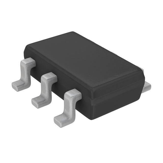
The MAX5432/MAX5433 are available in a 3mm x 3mm
8-pin TDFN package and the MAX5434/MAX5435 are
available in a 6-pin thin SOT23 package. The MAX5432–
MAX5435 are specified over the extended (-40°C to
+85°C) temperature range.
Applications
Features
♦ Tiny 3mm x 3mm 8-Pin TDFN and 6-Pin Thin
SOT23 Packages
♦ Power-On Recall of Wiper Position from
Nonvolatile Memory
♦ 35ppm/°C End-to-End Resistance Temperature
Coefficient
♦ 5ppm/°C Ratiometric Temperature Coefficient
♦ 50kΩ/100kΩ Resistor Values
♦ Fast 400kbps I2C-Compatible Serial Interface
♦ 500nA (typ) Static Supply Current
♦ +2.7V to +5.25V Single-Supply Operation
♦ 32 Tap Positions
♦ ±0.15 LSB INL (typ), ±0.15 LSB DNL (typ)
Pin Configurations
TOP VIEW
+
+
H 1
8 W
VDD 1
6
L
SDA 2
7 L
GND 2
5
W
4
SDA
GND 3
SCL 4
6 A0
MAX5432
MAX5433
SCL 3
5 VDD
MAX5434
MAX5435
SOT23
Mechanical Potentiometer Replacement
Low-Drift Programmable-Gain Amplifiers
Volume Control
Liquid-Crystal Display (LCD) Screen Adjustment
TDFN
Ordering Information/Selector Guide
PART
PIN-PACKAGE
TOP MARK
I2C ADDRESS
Ω)
R (kΩ
PKG CODE
MAX5432LETA+
8 TDFN-EP*
ANG
010100A0**
50
T833-1
MAX5432META+
8 TDFN-EP*
ANI
010110A0**
50
T833-1
MAX5433LETA+
8 TDFN-EP*
ANF
010100A0**
100
T833-1
MAX5433META+
8 TDFN-EP*
ANH
010110A0**
100
T833-1
MAX5434LEZT+T
6 Thin SOT23-6
AABX
0101000
50
Z6-1
*EP = Exposed pad.
**A0 represents the logic state of input A0 of the device in the TDFN package.
+Denotes a lead-free package.
T = Tape and reel.
Note: All devices are specified over the -40°C to +85°C operating temperature range.
Ordering Information/Selector Guide continued at end of data sheet.
________________________________________________________________ Maxim Integrated Products
For pricing, delivery, and ordering information, please contact Maxim Direct at 1-888-629-4642,
or visit Maxim’s website at www.maxim-ic.com.
1
MAX5432–MAX5435
General Description
�MAX5432–MAX5435
32-Tap, Nonvolatile, I2C, Linear, Digital
Potentiometers
ABSOLUTE MAXIMUM RATINGS
VDD to GND ...........................................................-0.3V to +6.0V
SDA, SCL to GND..................................................-0.3V to +6.0V
A0, H, L, and W to GND .............................-0.3V to (VDD + 0.3V)
Maximum Continuous Current into H, L, and W
MAX5432/MAX5434.....................................................±1.3mA
MAX5433/MAX5435.....................................................±0.6mA
Input/Output Latchup Immunity........................................±50mA
Continuous Power Dissipation (TA = +70°C)
6-Pin Thin SOT23 (derate 9.1mW/°C above +70°C) ....727mW
8-Pin TDFN (derate 18.2mW/°C above +70°C) ......1454.5mW
Operating Temperature Range ...........................-40°C to +85°C
Junction Temperature ......................................................+150°C
Storage Temperature Range .............................-60°C to +150°C
Lead Temperature (soldering, 10s) .................................+300°C
Stresses beyond those listed under “Absolute Maximum Ratings” may cause permanent damage to the device. These are stress ratings only, and functional
operation of the device at these or any other conditions beyond those indicated in the operational sections of the specifications is not implied. Exposure to
absolute maximum rating conditions for extended periods may affect device reliability.
ELECTRICAL CHARACTERISTICS
(VDD = +2.7V to +5.25V, VH = VDD, VL = GND, TA = -40°C to +85°C, unless otherwise noted. Typical values are at VDD = +5V, TA =
+25°C.) (Note 1)
PARAMETER
SYMBOL
CONDITIONS
MIN
TYP
MAX
UNITS
DC PERFORMANCE
Resolution
32
End-to-End Resistance
RH-L
End-to-End Resistance
Temperature Coefficient
TCR
37.5
50
62.5
MAX5433/MAX5435
75
100
125
Ratiometric Resistance
Temperature Coefficient
Variable resistor (Note 2)
Integral Nonlinearity
INL
Voltage-divider,
MAX5432/MAX5433 (Note 3)
Variable resistor (Note 2)
Differential Nonlinearity
DNL
Voltage-divider,
MAX5432/MAX5433 (Note 3)
Full-Scale Error (Note 4)
Zero-Scale Error (Note 5)
Wiper Resistance
Taps
MAX5432/MAX5434
35
ppm/°C
5
ppm/°C
VDD = 5V
±0.15
±0.5
VDD = 3V
±0.15
±0.5
VDD = 5V
±0.15
±0.5
VDD = 3V
±0.15
±0.5
VDD = 5V
±0.15
±0.5
VDD = 3V
±0.15
±0.5
VDD = 5V
±0.15
±0.5
VDD = 3V
±0.15
±0.5
MAX5432, 50kΩ
-0.5
MAX5433, 100kΩ
-0.5
MAX5432, 50kΩ
+0.5
MAX5433, 100kΩ
+0.5
RW
MAX5432/MAX5433 (Note 6)
Input High Voltage
VIH
(Note 7)
Input Low Voltage
VIL
(Note 7)
kΩ
610
1200
LSB
LSB
LSB
LSB
Ω
DIGITAL INPUTS
Input Leakage Current
Input Capacitance
2
0.7 x
VDD
V
0.3 x
VDD
ILEAK
±1
5
_______________________________________________________________________________________
V
µA
pF
�32-Tap, Nonvolatile, I2C, Linear, Digital
Potentiometers
(VDD = +2.7V to +5.25V, VH = VDD, VL = GND, TA = -40°C to +85°C, unless otherwise noted. Typical values are at VDD = +5V, TA =
+25°C.) (Note 1)
PARAMETER
SYMBOL
CONDITIONS
MIN
TYP
MAX
UNITS
DYNAMIC CHARACTERISTICS
-3dB Bandwidth (Note 8)
Wiper Settling Time (Note 9)
MAX5432/MAX5434
500
MAX5433/MAX5435
250
MAX5432/MAX5434
0.5
MAX5433/MAX5435
1.0
kHz
µs
NONVOLATILE MEMORY RELIABILITY
Data Retention
Endurance
TA = +85°C
50
TA = +25°C
200,000
TA = +85°C
50,000
Years
Stores
POWER SUPPLY
Power-Supply Voltage
VDD
Standby Current
IDD
Programming Current
2.70
5.25
V
Digital inputs = VDD or GND, TA = +25°C
0.5
2
µA
During nonvolatile write; digital inputs =
VDD or GND (Note 10)
200
900
µA
TIMING CHARACTERISTICS
(VDD = +2.7V to +5.25V, VH = VDD, VL = GND, TA = -40°C to +85°C, unless otherwise noted. Typical values are at VDD = +5V, TA =
+25°C.) (Figures 1 and 2) (Note 11)
PARAMETER
SCL Clock Frequency
SYMBOL
CONDITIONS
MIN
TYP
fSCL
MAX
UNITS
400
kHz
Setup Time for START Condition
tSU-STA
0.6
µs
Hold Time for START Condition
tHD-STA
0.6
µs
tHIGH
0.6
µs
CLK High Time
CLK Low Time
tLOW
1.3
µs
Data Setup Time
tSU-DAT
100
ns
Data Hold Time
tHD-DAT
0
0.9
µs
SDA, SCL Rise Time
tR
300
ns
SDA, SCL Fall Time
tF
300
ns
Setup Time for STOP Condition
tSU-STO
0.6
µs
Bus Free Time Between STOP
and START Condition
tBUF
1.3
µs
Pulse Width of Spike Suppressed
tSP
Capacitive Load for Each Bus
Line
CB
Nonvolatile Store Time
(Note 12)
Idle time required after a nonvolatile
memory write (Note 13)
50
ns
400
pF
12
ms
Note 1: All devices are production tested at TA = +25°C and are guaranteed by design and characterization for -40°C < TA < +85°C.
_______________________________________________________________________________________
3
MAX5432–MAX5435
ELECTRICAL CHARACTERISTICS (continued)
�TIMING CHARACTERISTICS (continued)
(VDD = +2.7V to +5.25V, VH = VDD, VL = GND, TA = -40°C to +85°C, unless otherwise noted. Typical values are at VDD = +5V, TA =
+25°C.) (Figures 1 and 2) (Note 1)
Note 2: The DNL and INL are measured with the potentiometer configured as a variable resistor. For the 3-terminal potentiometers
(MAX5432/MAX5433), H is unconnected and L = GND. At VDD = 5V, W is driven with a source current of 80µA for the 50kΩ
configuration, and 40µA for the 100kΩ configuration. At VDD = 3V, W is driven with a source current of 40µA for the 50kΩ
configuration, and 20µA for the 100kΩ configuration.
Note 3: The DNL and INL are measured with the potentiometer configured as a voltage-divider with H = VDD and L = GND
(MAX5432/MAX5433 only). The wiper terminal is unloaded and measured with an ideal voltmeter.
Note 4: Full-scale error is defined as
VW - VH
.
⎛ VH ⎞
⎜
⎟
⎝ 31 ⎠
Note 5: Zero-scale error is defined as
VW - VL
.
⎛ VH ⎞
⎜
⎟
⎝ 31 ⎠
Note 6: The wiper resistance is the worst value measured by injecting the currents given in Note 2 into W with L = GND.
RW = (VW - VH) / IW.
Note 7: The device draws current in excess of the specified supply current when the digital inputs are driven with voltages between
(VDD - 0.5V) and (GND + 0.5V). See the Supply Current vs. Digital Input Voltage graph in the Typical Operating Characteristics.
Note 8: Wiper is at midscale with a 10pF capacitive load. Potentiometer set to midscale, L = GND, an AC source is applied to H,
and the output is measured as 3dB lower than the DC W/H value in dB.
Note 9: This is measured from the STOP pulse to the time it takes the output to reach 50% of the output step size (divider mode). It
is measured with a maximum external capacitive load of 10pF.
Note 10: The programming current exists only during NV writes (12ms typ).
Note 11: Digital timing is guaranteed by design and characterization, and is not production tested.
Note 12: An appropriate bus pullup resistance must be selected depending on board capacitance. Refer to the I2C-bus specification document linked to this web address: www.semiconductors.philips.com/acrobat/literature/9398/39340011.pdf
Note 13: The idle time begins from the initiation of the stop pulse.
Typical Operating Characteristics
(VDD = +5V, TA = +25°C, unless otherwise noted.)
0.9
VDD = 5V
0.6
VDD = 3V
0.3
0.8
0.6
0.4
0.2
0
-15
10
35
TEMPERATURE (°C)
60
85
1000
VDD = 5V
100
10
VDD = 3V
1
0.1
0
-40
4
DIGITAL INPUTS = GND OR VDD
SUPPLY CURRENT (µA)
1.2
1.0
MAX5432–35 toc02
DIGITAL INPUTS = GND OR VDD
SUPPLY CURRENT (µA)
MAX5432–35 toc01
1.5
SUPPLY CURRENT
vs. DIGITAL INPUT VOLTAGE
SUPPLY CURRENT
vs. SUPPLY VOLTAGE
MAX5432–35 toc03
STANDBY SUPPLY CURRENT
vs. TEMPERATURE
SUPPLY CURRENT (µA)
MAX5432–MAX5435
32-Tap, Nonvolatile, I2C, Linear, Digital
Potentiometers
2.5
3.0
3.5
4.0
4.5
SUPPLY VOLTAGE (V)
5.0
5.5
0
1
2
3
DIGITAL INPUT VOLTAGE (V)
_______________________________________________________________________________________
4
5
�32-Tap, Nonvolatile, I2C, Linear, Digital
Potentiometers
END-TO-END RESISTANCE % CHANGE
vs. TEMPERATURE
0.5
0
-0.5
MAX5432–35 toc06
1.0
MAX5432-35 toc05
50kΩ
100kΩ
END-TO-END RESISTANCE % CHANGE
MAX5432–35 toc04
1.0
END-TO-END RESISTANCE CHANGE ( %)
TAP-TO-TAP SWITCHING TRANSIENT
(0 TO MIDSCALE, CL = 10pF)
END-TO-END RESISTANCE % CHANGE
vs. TEMPERATURE
0.5
SDA
2V/div
0
VW
1V/div
-0.5
50kΩ
-1.0
-40
-15
10
35
60
-1.0
85
-40
-15
TEMPERATURE (°C)
10
35
60
1µs/div
85
TEMPERATURE (°C)
TAP-TO-TAP SWITCHING TRANSIENT
(0 TO MIDSCALE, CL = 10pF)
MIDSCALE WIPER TRANSIENT
AT POWER-ON
WIPER TRANSIENT AT POWER-ON
MAX5432–35 toc08
MAX5432–35 toc07
MAX5432–35 toc09
VDD
2V/div
SDA
2V/div
VDD
2V/div
VW
1V/div
VW
1V/div
50kΩ
100kΩ
1µs/div
10µs/div
MIDSCALE WIPER RESPONSE
vs. FREQUENCY
(MAX5432)
MIDSCALE WIPER RESPONSE
vs. FREQUENCY (MAX5433)
GAIN (dB)
GAIN (dB)
-9
CW = 33pF
-9
CW = 33pF
-12
-12
-15
-15
VDD = 3V
600
RESISTANCE (Ω)
-6
-6
700
MAX5432–35 toc12
CW = 10pF
WIPER RESISTANCE vs. TAP POSITION
(MAX5432)
MAX5432–35 toc11
-3
CW = 10pF
-3
100kΩ
10µs/div
0
MAX5432 toc10
0
VW
1V/div
500
400
300
200
100
-18
-18
0.1
1
10
FREQUENCY (kHz)
100
1000
0
0.1
1
10
FREQUENCY (kHz)
100
1000
0
4
8
12
16
20
24
28
31
TAP POSITION
_______________________________________________________________________________________
5
MAX5432–MAX5435
Typical Operating Characteristics (continued)
(VDD = +5V, TA = +25°C, unless otherwise noted.)
�Typical Operating Characteristics (continued)
(VDD = +5V, TA = +25°C, unless otherwise noted.)
WIPER RESISTANCE vs. TAP POSITION
(MAX5432)
400
300
300
500
400
300
200
200
200
100
100
100
0
0
8
12
16
20
24
0
28 31
4
8
16
20
24
28
0
31
0
30
0.5
VARIABLE-RESISTOR MODE
MAX5432/MAX5434
0.4
0.3
RESISTANCE DNL (LSB)
MAX5432–35 toc16
100kΩ
60
50
40
0.2
0.1
0
-0.1
-0.2
0.1
0
-0.1
-0.2
-0.4
0
16
20
TAP POSITION
24
28 31
28 31
0.2
-0.5
12
24
0.3
10
8
20
VARIABLE-RESISTOR MODE
MAX5432/MAX5434
0.4
-0.3
4
16
RESISTANCE INL vs. TAP POSITION
-0.4
50kΩ
12
0.5
-0.3
0
8
TAP POSITION
RESISTANCE DNL vs. TAP POSITION
W-TO-L RESISTANCE vs. TAP POSITION
120
110
100
20
4
TAP POSITION
TAP POSITION
90
80
70
12
RESISTANCE INL (LSB)
4
MAX5432–35 toc17
0
6
VDD = 5V
600
500
400
MAX5432-35 toc15
600
RESISTANCE (Ω)
500
VDD = 5V
RESISTANCE (Ω)
600
700
MAX5432–35 toc14
VDD = 3V
RESISTANCE (Ω)
700
MAX5432-35 toc13
700
WIPER RESISTANCE vs. TAP POSITION
(MAX5433)
MAX5432–35 toc18
WIPER RESISTANCE vs. TAP POSITION
(MAX5433)
W-TO-L RESISTANCE (kΩ)
MAX5432–MAX5435
32-Tap, Nonvolatile, I2C, Linear, Digital
Potentiometers
-0.5
0
4
8
12
16
20
TAP POSITION
24
28 31
0
4
8
12
16
20
TAP POSITION
_______________________________________________________________________________________
24
28 31
�32-Tap, Nonvolatile, I2C, Linear, Digital
Potentiometers
0.1
0
-0.1
-0.2
0.2
0.1
0
-0.1
-0.2
0.2
0.1
0
-0.1
-0.2
-0.3
-0.3
-0.4
-0.4
-0.4
-0.5
-0.5
4
8
12
16
20
24
28 31
-0.5
0
4
8
TAP POSITION
RESISTANCE INL vs. TAP POSITION
16
20
24
28 31
0
0.1
0
-0.1
-0.2
VOLTAGE-DIVIDER MODE
MAX5433
0.4
0.3
0.2
0.1
0
-0.1
-0.2
0
-0.1
-0.2
-0.4
-0.5
20
TAP POSITION
24
28 31
28 31
0.1
-0.3
16
24
0.2
-0.4
12
20
0.3
-0.4
8
16
VOLTAGE-DIVIDER MODE
MAX5433
0.4
-0.3
-0.5
12
RESISTANCE INL vs. TAP POSITION
-0.3
4
8
0.5
RESISTANCE INL (LSB)
0.2
0.5
RESISTANCE DNL (LSB)
0.3
0
4
TAP POSITION
RESISTANCE DNL vs. TAP POSITION
MAX5432-35 toc22
VARIABLE-RESISTOR MODE
MAX5433/MAX5435
0.4
12
TAP POSITION
0.5
MAX5432-35 toc21
0.3
-0.3
0
RESISTANCE INL (LSB)
MAX5432–35 toc20
0.3
VARIABLE-RESISTOR MODE
MAX5433/MAX5435
0.4
MAX5432-35 toc24
0.2
RESISTANCE DNL vs. TAP POSITION
0.5
MAX5432-35 toc23
RESISTANCE DNL (LSB)
0.3
VOLTAGE-DIVIDER MODE
MAX5432
0.4
RESISTANCE INL (LSB)
MAX5432–35 toc19
VOLTAGE-DIVIDER MODE
MAX5432
0.4
RESISTANCE INL vs. TAP POSITION
0.5
RESISTANCE DNL (LSB)
RESISTANCE DNL vs. TAP POSITION
0.5
-0.5
0
4
8
12
16
20
TAP POSITION
24
28 31
0
4
8
12
16
20
24
28 31
TAP POSITION
_______________________________________________________________________________________
7
MAX5432–MAX5435
Typical Operating Characteristics (continued)
(VDD = +5V, TA = +25°C, unless otherwise noted.)
�32-Tap, Nonvolatile, I2C, Linear, Digital
Potentiometers
MAX5432–MAX5435
Pin Description
PIN
FUNCTION
NAME
TDFN
THIN SOT23
1
—
H
2
4
SDA
3
2
GND
Ground
4
3
SCL
I2C-Compatible Interface Clock Input
5
1
VDD
Power-Supply Input. Bypass with a 0.1µF capacitor from VDD to GND.
6
—
A0
7
6
L
Low Terminal
8
5
W
Wiper Terminal
EP
—
EP
Exposed Pad. Internally connected to GND.
High Terminal
I2C-Compatible Interface Data Input
Address Input. Sets the I2C address. Connect to VDD or GND. Do not leave A0 floating.
Detailed Description
The MAX5432–MAX5435 contain a resistor array with
31 resistive elements. The MAX5432/MAX5434 provide
a total end-to-end resistance of 50kΩ, and the
MAX5433/MAX5435 provide an end-to-end resistance
of 100kΩ.
The MAX5432/MAX5433 allow access to the high, low,
and wiper terminals for a standard voltage-divider configuration. Connect H, L, and W in any desired configuration as long as their voltages fall between GND and
V DD. The MAX5434/MAX5435 are variable resistors
with H internally connected to the wiper.
A simple 2-wire I2C-compatible serial interface moves
the wiper among the 32 tap points. Eight data bits, an
address byte, and a control byte program the wiper
position. A nonvolatile memory stores and recalls the
wiper position in the nonvolatile memory upon power-up.
The nonvolatile memory is guaranteed for 200,000 wiper
store cycles and 50 years for wiper data retention.
Digital Interface
The MAX5432–MAX5435 feature an internal, nonvolatile
EEPROM that returns the wiper to its previously stored
position at power-up. The shift register decodes the
control and address bits, routing the data to the proper
memory registers. Write data to the volatile memory
register to immediately update the wiper position, or
write data to the nonvolatile register for storage. Writing
to the nonvolatile register takes a minimum of 12ms.
The volatile register retains data as long as the device
is enabled and powered. Removing power clears the
volatile register. The nonvolatile register retains data
even after power is removed. Upon power-up, the
8
power-on reset circuitry and internal oscillator control
the transfer of data from the nonvolatile register to the
volatile register.
Serial Addressing
The MAX5432–MAX5435 operate as a slave that sends
and receives data through an I2C- and SMBus™-compatible 2-wire interface. The interface uses a serial data
access (SDA) line and a serial clock line (SCL) to
achieve bidirectional communication between
master(s) and slave(s). A master, typically a microcontroller, initiates all data transfers to and from the
MAX5432–MAX5435, and generates the SCL clock that
synchronizes the data transfer (Figure 1).
SDA operates as both an input and an open-drain output. SDA requires a pullup resistor, typically 4.7kΩ.
SCL only operates as an input. SCL requires a pullup
resistor (4.7kΩ typ) if there are multiple masters on the
2-wire interface, or if the master in a single-master system has an open-drain SCL output.
Each transmission consists of a START (S) condition
(Figure 3) sent by a master, followed by the
MAX5432–MAX5435 7-bit slave address plus the 8th bit
(Figure 4), 1 command byte (Figure 7) and 1 data byte,
and finally a STOP (P) condition (Figure 3).
Start and Stop Conditions
Both SCL and SDA remain high when the interface is
not busy. A master signals the beginning of a transmission with a START (S) condition by transitioning SDA
from high to low while SCL is high. When the master
has finished communicating with the slave, it issues a
STOP (P) condition by transitioning the SDA from low to
SMBus is a trademark of Intel Corporation.
_______________________________________________________________________________________
�32-Tap, Nonvolatile, I2C, Linear, Digital
Potentiometers
MAX5432–MAX5435
tF
tR
SDA
tSU-DAT
tHD-DAT
tLOW
tBUF
tHD-STA
tSU-STA
tSU-STO
SCL
tHIGH
tHD-STA
tR
tF
S
Sr
A
P
S
PARAMETERS ARE MEASURED FROM 30% TO 70%.
Figure 1. I2C Serial-Interface Timing Diagram
high while SCL is high. The bus is then free for another
transmission (Figure 3).
Bit Transfer
One data bit is transferred during each clock pulse.
The data on the SDA line must remain stable while SCL
is high (Figure 5).
Acknowledge
The acknowledge bit is a clocked 9th bit that the recipient uses to handshake receipt of each byte of data
(Figure 6). Each byte transferred effectively requires 9
bits. The master generates the 9th clock pulse, and the
recipient pulls down SDA during the acknowledge
clock pulse, so the SDA line is stable low during the
high period of the clock pulse. When the master transmits to the MAX5432–MAX5435, the devices generate
the acknowledge bit because the MAX5432–MAX5435
are the recipients.
Slave Address
The MAX5432–MAX5435 have a 7-bit-long slave
address (Figure 4). The 8th bit following the 7-bit slave
address is the NOP/W bit. Set the NOP/W bit low for a
write command and high for a no-operation command.
Table 1a shows four possible slave addresses for the
MAX5432/MAX5433 and Table 1b shows three possible
slave addresses for the MAX5434/MAX5435. The first 4
bits (MSBs) of the slave addresses are always 0101.
Bits A2 and A1 are factory programmed for the
MAX5432/MAX5433 (Table 1a). Connect the A0 input
(MAX5432/MAX5433 only) to either GND or V DD to
select one of two I2C device addresses. Each device
must have a unique address to share the bus. A maximum of four MAX5432/MAX5433 devices can share the
same bus. Bits A2, A1, and A0 are factory programmed
for the MAX5434/MAX5435 (Table 1b).
Table 1a. Address Codes
(MAX5432/MAX5433 Only)
ADDRESS BYTE
PART
SUFFIX
A6
A5
A4
A3
A2
A1
A0
NOP/W
L
0
1
0
1
0
0
0
NOP/W
L
0
1
0
1
0
0
1
NOP/W
M
0
1
0
1
1
0
0
NOP/W
M
0
1
0
1
1
0
1
NOP/W
Table 1b. Address Codes
(MAX5434/MAX5435 Only)
ADDRESS BYTE
PART
SUFFIX
A6
A5
A4
A3
A2
A1
A0
NOP/W
L
0
1
0
1
0
0
0
NOP/W
M
0
1
0
1
1
0
0
NOP/W
N*
0
1
0
1
0
1
0
NOP/W
*MAX5434 only.
Message Format for Writing
A write to the MAX5432–MAX5435 consists of the transmission of the device’s slave address with the 8th bit set
to zero, followed by at least 1 byte of information. The
1st byte of information is the command byte. The bytes
received after the command byte are the data bytes.
The 1st data byte goes into the internal register of the
MAX5432–MAX5435 as selected by the command byte
(Figure 8).
_______________________________________________________________________________________
9
�VDD
IOL = 3mA
SDA
VOUT
SDA
SCL
400pF
IOH = 0mA
Figure 2. Load Circuit
SDA
S
P
START
CONDITION
STOP
CONDITION
Figure 3. Start and Stop Conditions
0
1
0
1
0*
0*
A0
MSB
NOP/W
ACK
LSB
SCL
*SEE THE Ordering Information/Selector Guide FOR OTHER ADDRESS OPTIONS.
Figure 4. Slave Address
Command Byte
Use the command byte to select the destination of the
wiper data (nonvolatile or volatile memory registers)
and swap data between nonvolatile and volatile memory registers (see Table 2).
Command Descriptions
VREG: The data byte writes to the volatile memory register and the wiper position updates with the data in the
volatile memory register.
NVREG: The data byte writes to the nonvolatile memory
register. The wiper position is unchanged.
Data Byte
The MAX5432–MAX5435 use the first 5 bits (MSBs,
D7–D3) of the data byte to set the position of the wiper.
The last 3 bits (D2, D1, and D0) are don’t care bits (see
Table 2).
NVREGxVREG: Data transfers from the nonvolatile
memory register to the volatile memory register (wiper
position updates).
VREGxNVREG: Data transfers from the volatile memory
register into the nonvolatile memory register.
Table 2. Command Byte Summary
ADDRESS BYTE
1
2
3
4
5
6
COMMAND BTYE
7
8
DATA BYTE
9
10 11 12 13 14 15 16 17 18 19 20 21 22 23 24 25 26 27
A
C
K
A
C7 C6 C5 C4 C3 C2 C1 C0 C
K
D7 D6 D5 D4 D3 D2 D1 D0
VREG
0
1
0
1
A2 A1 A0
N
O
P/
W
0
0
0
0
1
0
0
0
1
D7 D6 D5 D4 D3
X
X
X
NVREG
0
1
0
1
A2 A1 A0
0
0
0
1
0
0
0
0
1
D7 D6 D5 D4 D3
X
X
X
NVREGxVREG
0
1
0
1
A2 A1 A0
0
0
1
1
0
0
0
0
1
D7 D6 D5 D4 D3
X
X
X
VREGxNVREG
0
1
0
1
A2 A1 A0
0
0
1
0
1
0
0
0
1
D7 D6 D5 D4 D3
X
X
X
SCL CYCLE
NUMBER
A6 A5 A4 A3 A2 A1 A0
X = Don’t care.
10
______________________________________________________________________________________
A
C
K
STOP
REGISTER
START
MAX5432–MAX5435
32-Tap, Nonvolatile, I2C, Linear, Digital
Potentiometers
�32-Tap, Nonvolatile, I2C, Linear, Digital
Potentiometers
SDA
MAX5432–MAX5435
CLOCK PULSE FOR
ACKNOWLEDGMENT
START
CONDITION
SCL
1
2
8
9
NOT ACKNOWLEDGE
SCL
DATA STABLE,
DATA VALID
SDA
CHANGE OF
DATA ALLOWED
ACKNOWLEDGE
Figure 6. Acknowledge
Figure 5. Bit Transfer
COMMAND BYTE IS STORED ON
RECEIPT OF STOP CONDITION
SLAVE
ADDRESS
S
D15
ACKNOWLEDGE FROM
MAX5432–MAX5435
0
D14
D13
A
D11
D12
D10
D9
D8
A
COMMAND BYTE
P
ACKNOWLEDGE FROM
MAX5432–MAX5435
NOP/W
Figure 7. Command Byte Received
ACKNOWLEDGE FROM
MAX5432–MAX5435
ACKNOWLEDGE FROM
MAX5432–MAX5435
HOW COMMAND BYTE AND DATA BYTE MAP
INTO MAX5432–MAX5435's REGISTERS
ACKNOWLEDGE FROM
MAX5432–MAX5435
S
D15 D14 D13 D12 D11 D10
0
SLAVE ADDRESS
A
COMMAND BYTE
D9
D8
D7
A
D6
D5
D4
D3
DATA BYTE
X
X
X
A
P
1
BYTE
NOP/W
Figure 8. Command and Single Data Byte Received
Nonvolatile Memory
The internal EEPROM consists of a 5-bit nonvolatile
register that retains the value written to it before the
device is powered down. The nonvolatile register is
programmed with the zeros at the factory. Wait a minimum of 12ms after writing to NVREG before sending
another command.
with the data stored in the nonvolatile memory register.
This initialization period takes 20µs.
Standby
The MAX5432–MAX5435 feature a low-power standby
mode. When the device is not being programmed, it
goes into standby mode and current consumption is
typically 0.5µA.
Power-Up
Upon power-up, the MAX5432–MAX5435 load the data
stored in the nonvolatile memory register into the
volatile memory register, updating the wiper position
______________________________________________________________________________________
11
�MAX5432–MAX5435
32-Tap, Nonvolatile, I2C, Linear, Digital
Potentiometers
5V
5V
H
30V
30V
W
MAX5432
MAX5433
VOUT
L
VOUT
H
MAX5432–
MAX5435
W
L
Figure 9. Positive LCD Bias Control Using a Voltage-Divider
Figure 10. Positive LCD Bias Control Using a Variable Resistor
+5V
W
VIN
L
H
VIN
R3
C
VOUT
V0 REF
OUT
H
R1
MAX6160
R1
ADJ
W
GND
H
MAX5432–
MAX5435
R2
W
L
MAX5432
MAX5433
R2
L
V0 = 1.23V
50kΩ
FOR THE MAX5432
R2(kΩ)
V0 = 1.23V
100kΩ
FOR THE MAX5433
R2(kΩ)
Figure 12. Adjustable Voltage Reference
Figure 11. Programmable Filter
Applications Information
Use the MAX5432–MAX5435 in applications requiring
digitally controlled adjustable resistance, such as LCD
contrast control (where voltage biasing adjusts the display contrast), or for programmable filters with
adjustable gain and/or cutoff frequency.
Positive LCD Bias Control
Figures 9 and 10 show an application where the voltage-divider or variable resistor is used to make an
adjustable, positive LCD bias voltage. The op-amp provides buffering and gain to the resistor-divider network
made by the potentiometer (Figure 9) or to a fixed
resistor and a variable resistor (Figure 10).
R2, and the cutoff frequency is adjusted by R3. Use the
following equations to calculate the gain (G) and the
3dB cutoff frequency (fC).
R1
R2
1
fC =
2π × R 3 × C
G = 1+
Adjustable Voltage Reference
Figure 12 shows the MAX5432/MAX5433 used as the
feedback resistors in an adjustable voltage reference
application. Independently adjust the output voltages of
the MAX6160 from 1.23V to (VIN - 0.2V) by changing
the wiper position of the MAX5432/MAX5433.
Programmable Filter
Figure 11 shows the configuration for a 1st-order programmable filter. The gain of the filter is adjusted by
12
______________________________________________________________________________________
�32-Tap, Nonvolatile, I2C, Linear, Digital
Potentiometers
H
VDD
GND
SDA
SCL
5-BIT
SHIFT
REGISTER
5-BIT
LATCH
5
5
32POSITION
DECODER
32
W
L
POR
I2C
INTERFACE
5-BIT
NV
MEMORY
MAX5432
MAX5433
A0
MAX5434/MAX5435 Functional Diagram
VDD
GND
SDA
SCL
5-BIT
SHIFT
REGISTER
I2C
INTERFACE
5-BIT
LATCH
5
5
32POSITION
DECODER
32
W
L
POR
5-BIT
NV
MEMORY
MAX5434
MAX5435
______________________________________________________________________________________
13
MAX5432–MAX5435
MAX5432/MAX5433 Functional Diagram
�MAX5432–MAX5435
32-Tap, Nonvolatile, I2C, Linear, Digital
Potentiometers
Ordering Information/Selector Guide (continued)
PART
MAX5434MEZT+T
PIN-PACKAGE
TOP MARK
I2C ADDRESS
Ω)
R (kΩ
PKG CODE
6 Thin SOT23-6
AABY
0101100
50
Z6-1
Z6-1
MAX5434NEZT+T
6 Thin SOT23-6
AABS
0101010
50
MAX5435LEZT+T
6 Thin SOT23-6
AABW
0101000
100
Z6-1
MAX5435MEZT+T
6 Thin SOT23-6
AABV
0101100
100
Z6-1
*EP = Exposed pad.
**A0 represents the logic state of input A0 of the device in the TDFN package.
+Denotes a lead-free package.
T = Tape and reel.
Note: All devices are specified over the -40°C to +85°C operating temperature range.
Chip Information
TRANSISTOR COUNT: 7817
PROCESS: BiCMOS
14
______________________________________________________________________________________
�32-Tap, Nonvolatile, I2C, Linear, Digital
Potentiometers
6, 8, &10L, DFN THIN.EPS
______________________________________________________________________________________
15
MAX5432–MAX5435
Package Information
(The package drawing(s) in this data sheet may not reflect the most current specifications. For the latest package outline information,
go to www.maxim-ic.com/packages.)
�MAX5432–MAX5435
32-Tap, Nonvolatile, I2C, Linear, Digital
Potentiometers
Package Information (continued)
(The package drawing(s) in this data sheet may not reflect the most current specifications. For the latest package outline information,
go to www.maxim-ic.com/packages.)
16
COMMON DIMENSIONS
PACKAGE VARIATIONS
SYMBOL
MIN.
MAX.
PKG. CODE
N
D2
E2
e
JEDEC SPEC
b
[(N/2)-1] x e
A
0.70
0.80
T633-2
6
1.50±0.10
2.30±0.10
0.95 BSC
MO229 / WEEA
0.40±0.05
1.90 REF
D
2.90
3.10
T833-2
8
1.50±0.10
2.30±0.10
0.65 BSC
MO229 / WEEC
0.30±0.05
1.95 REF
E
2.90
3.10
T833-3
8
1.50±0.10
2.30±0.10
0.65 BSC
MO229 / WEEC
0.30±0.05
1.95 REF
A1
0.00
0.05
T1033-1
10
1.50±0.10
2.30±0.10
0.50 BSC
MO229 / WEED-3
0.25±0.05
2.00 REF
L
0.20
0.40
T1033-2
10
1.50±0.10
2.30±0.10
0.50 BSC
MO229 / WEED-3
0.25±0.05
2.00 REF
k
0.25 MIN.
T1433-1
14
1.70±0.10
2.30±0.10
0.40 BSC
----
0.20±0.05
2.40 REF
A2
0.20 REF.
T1433-2
14
1.70±0.10
2.30±0.10
0.40 BSC
----
0.20±0.05
2.40 REF
______________________________________________________________________________________
�32-Tap, Nonvolatile, I2C, Linear, Digital
Potentiometers
6L THIN SOT23.EPS
______________________________________________________________________________________
17
MAX5432–MAX5435
Package Information (continued)
(The package drawing(s) in this data sheet may not reflect the most current specifications. For the latest package outline information,
go to www.maxim-ic.com/packages.)
�MAX5432–MAX5435
32-Tap, Nonvolatile, I2C, Linear, Digital
Potentiometers
Package Information (continued)
(The package drawing(s) in this data sheet may not reflect the most current specifications. For the latest package outline information,
go to www.maxim-ic.com/packages.)
18
______________________________________________________________________________________
�32-Tap, Nonvolatile, I2C, Linear, Digital
Potentiometers
REVISION
NUMBER
REVISION
DATE
3
11/07
DESCRIPTION
Eliminated address options, added lead-free option, updated information in Table 1b
PAGES
CHANGED
1, 9, 14
Maxim cannot assume responsibility for use of any circuitry other than circuitry entirely embodied in a Maxim product. No circuit patent licenses are
implied. Maxim reserves the right to change the circuitry and specifications without notice at any time.
Maxim Integrated Products, 120 San Gabriel Drive, Sunnyvale, CA 94086 408-737-7600 ____________________ 19
© 2007 Maxim Integrated Products
is a registered trademark of Maxim Integrated Products, Inc.
MAX5432–MAX5435
Revision History
�


 工商网监
湘ICP备2023018690号
工商网监
湘ICP备2023018690号
