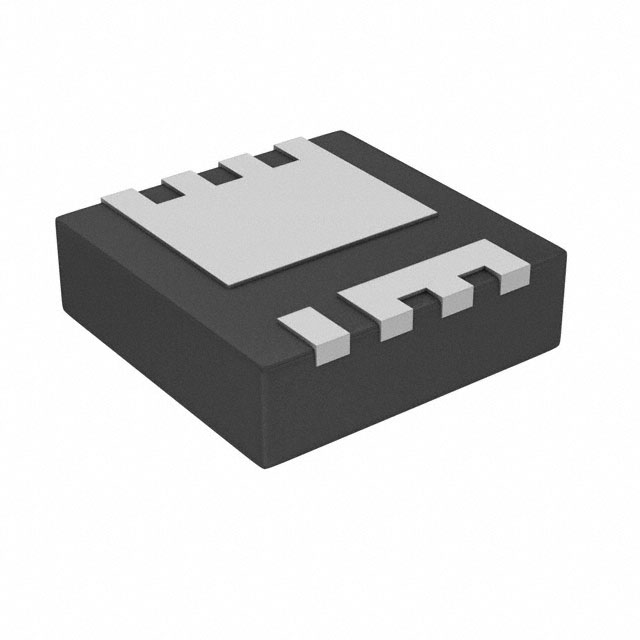
BSZ011NE2LS5I
MOSFET
OptiMOSTM5�Power-Transistor,�25�V
TSDSON-8�FL
(enlarged source interconnection)
Features
•�Optimized�for�high�performance�buck�converters
•�Monolithic�integrated�Schottky-like�diode
•�Very�low�on-resistance�RDS(on)�@�VGS=4.5V
•�100%�avalanche�tested
•�N-channel
•�Pb-free�lead�plating;�RoHS�compliant
•�Halogen-free�according�to�IEC61249-2-21
Product�validation
Fully�qualified�according�to�JEDEC�for�Industrial�Applications
Table�1�����Key�Performance�Parameters
S1
8D
S2
7D
Parameter
Value
Unit
S3
6D
VDS
25
V
G4
5D
RDS(on),max
1.1
mΩ
ID
202
A
Qoss
29
nC
QG(0V..4.5V)
17
nC
Type�/�Ordering�Code
Package
Marking
Related�Links
BSZ011NE2LS5I
PG-TSDSON-8 FL
11NE25I
-
Final Data Sheet
1
Rev.�2.1,��2020-10-23
�OptiMOSTM5�Power-Transistor,�25�V
BSZ011NE2LS5I
Table�of�Contents
Description . . . . . . . . . . . . . . . . . . . . . . . . . . . . . . . . . . . . . . . . . . . . . . . . . . . . . . . . . . . . . . . . . . . . . . . . . . . . . 1
Maximum ratings . . . . . . . . . . . . . . . . . . . . . . . . . . . . . . . . . . . . . . . . . . . . . . . . . . . . . . . . . . . . . . . . . . . . . . . . 3
Thermal characteristics . . . . . . . . . . . . . . . . . . . . . . . . . . . . . . . . . . . . . . . . . . . . . . . . . . . . . . . . . . . . . . . . . . . . 3
Electrical characteristics . . . . . . . . . . . . . . . . . . . . . . . . . . . . . . . . . . . . . . . . . . . . . . . . . . . . . . . . . . . . . . . . . . . 4
Electrical characteristics diagrams . . . . . . . . . . . . . . . . . . . . . . . . . . . . . . . . . . . . . . . . . . . . . . . . . . . . . . . . . . . 6
Package Outlines . . . . . . . . . . . . . . . . . . . . . . . . . . . . . . . . . . . . . . . . . . . . . . . . . . . . . . . . . . . . . . . . . . . . . . . 10
Revision History . . . . . . . . . . . . . . . . . . . . . . . . . . . . . . . . . . . . . . . . . . . . . . . . . . . . . . . . . . . . . . . . . . . . . . . . 11
Trademarks . . . . . . . . . . . . . . . . . . . . . . . . . . . . . . . . . . . . . . . . . . . . . . . . . . . . . . . . . . . . . . . . . . . . . . . . . . . 11
Disclaimer . . . . . . . . . . . . . . . . . . . . . . . . . . . . . . . . . . . . . . . . . . . . . . . . . . . . . . . . . . . . . . . . . . . . . . . . . . . . 11
Final Data Sheet
2
Rev.�2.1,��2020-10-23
�OptiMOSTM5�Power-Transistor,�25�V
BSZ011NE2LS5I
1�����Maximum�ratings
at�TA=25�°C,�unless�otherwise�specified
Table�2�����Maximum�ratings
Parameter
Symbol
Values
Unit
Note�/�Test�Condition
202
128
173
109
35
A
VGS=10�V,�TC=25�°C
VGS=10�V,�TC=100�°C
VGS=4.5�V,�TC=25�°C
VGS=4.5�V,�TC=100�°C
VGS=10�V,�TA=25�°C,
RTHJA=60�°C/W2)
-
808
A
TC=25�°C
-
-
119
mJ
ID=20�A,�RGS=25�Ω
VGS
-16
-
16
V
-
Power dissipation
Ptot
-
-
69
2.1
W
TC=25�°C
TA=25�°C,�RTHJA=60�°C/W2)
Operating and storage temperature
Tj,�Tstg
-55
-
150
°C
IEC climatic category; DIN IEC 68-1:
55/150/56
Unit
Note�/�Test�Condition
Min.
Typ.
Max.
ID
-
-
ID,pulse
-
Avalanche energy, single pulse
EAS
Gate source voltage
Continuous drain current1)
Pulsed drain current3)
4)
2�����Thermal�characteristics
Table�3�����Thermal�characteristics
Parameter
Symbol
Thermal resistance, junction - case,
bottom
Values
Min.
Typ.
Max.
RthJC
-
-
1.8
°C/W -
Thermal resistance, junction - case,
top
RthJC
-
-
20
°C/W -
Device on PCB,
6 cm² cooling area
RthJA
-
-
60
°C/W -
1)
Rating refers to the product only with datasheet specified absolute maximum values, maintaining case temperature
at 25°C. For higher case temperature please refer to Diagram 2. De-rating will be required based on the actual
environmental conditions.
2)
Device on 40 mm x 40 mm x 1.5 mm epoxy PCB FR4 with 6 cm2 (one layer, 70 µm thick) copper area for drain
connection. PCB is vertical in still air.
3)
See Diagram 3 for more detailed information
4)
See Diagram 13 for more detailed information
Final Data Sheet
3
Rev.�2.1,��2020-10-23
�OptiMOSTM5�Power-Transistor,�25�V
BSZ011NE2LS5I
3�����Electrical�characteristics
at�Tj=25�°C,�unless�otherwise�specified
Table�4�����Static�characteristics
Parameter
Symbol
Drain-source breakdown voltage
V(BR)DSS
Breakdown voltage temperature
coefficient
Values
Unit
Note�/�Test�Condition
-
V
VGS=0�V,�ID=10�mA
15
-
mV/°C ID=10�mA,�referenced�to�25�°C
1.2
-
2
V
VDS=VGS,�ID=250�µA
IDSS
-
0.9
0.5
-
mA
VDS=20�V,�VGS=0�V,�Tj=25�°C
VDS=20�V,�VGS=0�V,�Tj=125�°C
Gate-source leakage current
IGSS
-
10
100
nA
VGS=20�V,�VDS=0�V
Drain-source on-state resistance
RDS(on)
-
0.82
1.1
1.1
1.5
mΩ
VGS=10�V,�ID=20�A
VGS=4.5�V,�ID=20�A
Gate resistance
RG
-
0.7
1.2
Ω
-
Transconductance
gfs
80
160
-
S
|VDS|≥2|ID|RDS(on)max,�ID=20�A
Unit
Note�/�Test�Condition
Min.
Typ.
Max.
25
-
dV(BR)DSS�/dTj -
Gate threshold voltage
VGS(th)
Zero gate voltage drain current
Table�5�����Dynamic�characteristics
Parameter
Symbol
Values
Min.
Typ.
Max.
Ciss
-
2500
3400
pF
VGS=0�V,�VDS=12�V,�f=1�MHz
Output capacitance
Coss
-
1200
1600
pF
VGS=0�V,�VDS=12�V,�f=1�MHz
Reverse transfer capacitance
Crss
-
92
-
pF
VGS=0�V,�VDS=12�V,�f=1�MHz
Turn-on delay time
td(on)
-
5
-
ns
VDD=12�V,�VGS=10�V,�ID=20�A,
RG,ext=1.6�Ω
Rise time
tr
-
4
-
ns
VDD=12�V,�VGS=10�V,�ID=20�A,
RG,ext=1.6�Ω
Turn-off delay time
td(off)
-
26
-
ns
VDD=12�V,�VGS=10�V,�ID=20�A,
RG,ext=1.6�Ω
Fall time
tf
-
3
-
ns
VDD=12�V,�VGS=10�V,�ID=20�A,
RG,ext=1.6�Ω
Input capacitance1)
1)
1)
Defined by design. Not subject to production test.
Final Data Sheet
4
Rev.�2.1,��2020-10-23
�OptiMOSTM5�Power-Transistor,�25�V
BSZ011NE2LS5I
Table�6�����Gate�charge�characteristics1)�
Parameter
Symbol
Gate to source charge
Values
Unit
Note�/�Test�Condition
-
nC
VDD=12�V,�ID=20�A,�VGS=0�to�4.5�V
3.5
-
nC
VDD=12�V,�ID=20�A,�VGS=0�to�4.5�V
-
3.5
-
nC
VDD=12�V,�ID=20�A,�VGS=0�to�4.5�V
Qsw
-
5.7
-
nC
VDD=12�V,�ID=20�A,�VGS=0�to�4.5�V
Gate charge total
Qg
-
17
23
nC
VDD=12�V,�ID=20�A,�VGS=0�to�4.5�V
Gate plateau voltage
Vplateau
-
2.3
-
V
VDD=12�V,�ID=20�A,�VGS=0�to�4.5�V
Gate charge total
Qg
-
37
50
nC
VDD=12�V,�ID=20�A,�VGS=0�to�10�V
Gate charge total, sync. FET
Qg(sync)
-
16
-
nC
VDS=0.1�V,�VGS=0�to�4.5�V
Qoss
-
29
38
nC
VDD=12�V,�VGS=0�V
Unit
Note�/�Test�Condition
Min.
Typ.
Max.
Qgs
-
5.6
Gate charge at threshold
Qg(th)
-
Gate to drain charge
Qgd
Switching charge
2)
2)
2)
Output charge
Table�7�����Reverse�diode
Parameter
Symbol
Diode continuous forward current
Values
Min.
Typ.
Max.
IS
-
-
107
A
TC=25�°C
Diode pulse current
IS,pulse
-
-
808
A
TC=25�°C
Diode forward voltage
VSD
-
0.50
0.65
V
VGS=0�V,�IF=11�A,�Tj=25�°C
Reverse recovery time
trr
-
19
-
ns
VR=20�V,�IF=20�A,�diF/dt=400�A/µs
Reverse recovery charge
Qrr
-
20
-
nC
VR=20�V,�IF=20�A,�diF/dt=400�A/µs
1)
2)
See ″Gate charge waveforms″ for parameter definition
Defined by design. Not subject to production test.
Final Data Sheet
5
Rev.�2.1,��2020-10-23
�OptiMOSTM5�Power-Transistor,�25�V
BSZ011NE2LS5I
4�����Electrical�characteristics�diagrams
Diagram�1:�Power�dissipation
Diagram�2:�Drain�current
70
250
60
200
150
40
ID�[A]
Ptot�[W]
50
30
100
20
50
10
0
0
20
40
60
80
100
120
140
0
160
0
20
40
60
TC�[°C]
80
100
120
140
160
TC�[°C]
Ptot=f(TC)
ID=f(TC);�VGS≥10�V
Diagram�3:�Safe�operating�area
Diagram�4:�Max.�transient�thermal�impedance
3
101
10
single pulse
0.01
0.02
0.05
0.1
0.2
0.5
1 µs
10 µs
102
100 µs
100
ZthJC�[K/W]
ID�[A]
101
1 ms
DC
10 ms
100
10-1
10-1
10-2
10-1
100
101
102
10-2
10-5
10-4
VDS�[V]
10-2
10-1
100
tp�[s]
ID=f(VDS);�TC=25�°C;�D=0;�parameter:�tp
Final Data Sheet
10-3
ZthJC=f(tp);�parameter:�D=tp/T
6
Rev.�2.1,��2020-10-23
�OptiMOSTM5�Power-Transistor,�25�V
BSZ011NE2LS5I
Diagram�5:�Typ.�output�characteristics
160
140
Diagram�6:�Typ.�drain-source�on�resistance
2.5
2.8 V
10 V
4.5 V
3V
2.0
3V
1.5
3.3 V
120
ID�[A]
3.3 V
80
2.5 V
60
RDS(on)��[mΩ]
100
4.5 V
1.0
10 V
40
0.5
20
0
0.0
0.5
1.0
1.5
2.0
2.5
0.0
3.0
0
10
20
VDS�[V]
30
40
ID�[A]
ID=f(VDS),�Tj=25�°C;�parameter:�VGS
RDS(on)=f(ID),�Tj=25�°C;�parameter:�VGS
Diagram�7:�Typ.�transfer�characteristics
Diagram�8:�Typ.�drain-source�on�resistance
160
2.5
140
2.0
120
RDS(on)��[mΩ]
ID�[A]
100
80
60
1.5
150 °C
1.0
25 °C
40
0.5
20
150 °C
25 °C
0
0.0
0.5
1.0
1.5
2.0
2.5
3.0
3.5
4.0
VGS�[V]
0
2
4
6
8
10
VGS�[V]
ID=f(VGS),�|VDS|>2|ID|RDS(on)max;�parameter:�Tj
Final Data Sheet
0.0
RDS(on)=f(VGS),�ID=20�A;�parameter:�Tj
7
Rev.�2.1,��2020-10-23
�OptiMOSTM5�Power-Transistor,�25�V
BSZ011NE2LS5I
Diagram�10:�Typ.�gate�threshold�voltage
1.6
2.00
1.4
1.75
1.2
1.50
1.0
1.25
VGS(th)�[V]
RDS(on)�(normalized�to�25�°C)
Diagram�9:�Normalized�drain-source�on�resistance
0.8
1.00
0.6
0.75
0.4
0.50
0.2
0.25
0.0
-80
-40
0
40
80
120
0.00
-80
160
-40
0
40
Tj�[°C]
80
120
160
Tj�[°C]
RDS(on)=f(Tj),�ID=20�A,�VGS=10�V
VGS(th)=f(Tj),�VGS=VDS,�ID=10�mA
Diagram�11:�Typ.�capacitances
Diagram�12:�Forward�characteristics�of�reverse�diode
4
103
10
-55°C, typ
25°C, typ
100°C, typ
150°C, typ
Ciss
103
102
IF�[A]
C�[pF]
Coss
102
101
Crss
101
0
5
10
15
20
25
100
0.0
0.2
VDS�[V]
0.6
0.8
1.0
VSD�[V]
C=f(VDS);�VGS=0�V;�f=1�MHz
Final Data Sheet
0.4
IF=f(VSD);�parameter:�Tj
8
Rev.�2.1,��2020-10-23
�OptiMOSTM5�Power-Transistor,�25�V
BSZ011NE2LS5I
Diagram�13:�Avalanche�characteristics
Diagram�14:�Typ.�gate�charge
2
10
10
5V
12 V
20 V
8
101
25 °C
VGS�[V]
IAV�[A]
6
100 °C
4
125 °C
0
10
2
10-1
100
101
102
103
tAV�[µs]
0
0
5
10
15
20
25
30
35
40
Qgate�[nC]
IAS=f(tAV);�RGS=25�Ω;�parameter:�Tj,start
VGS=f(Qgate),�ID=20�A�pulsed,�Tj=25�°C;�parameter:�VDD
Diagram�15:�Typ.�drain-source�leakage�current
Diagram Gate charge waveforms
-3
10
125 °C
IDSS�[A]
10-4
100 °C
75 °C
10-5
25 °C
-6
10
0
5
10
15
20
VDS�[V]
IDSS=f(VDS),�VGS=0�V;�parameter:�Tj
Final Data Sheet
9
Rev.�2.1,��2020-10-23
�OptiMOSTM5�Power-Transistor,�25�V
BSZ011NE2LS5I
5�����Package�Outlines
TSDSON-8-25/-26
j
DIM
A
b
b1
b2
D=D1
D2
D3
D4
E
E4
E6
e
N
L
L1
L2
aaa
F1
F2
F3
F4
F5
F6
F7
F8
F9
MILLIMETERS
MIN
0.90
0.24
0.10
0.24
3.20
2.19
1.54
0.21
3.20
2.01
0.10
0.30
0.40
0.50
MAX
1.10
0.44
0.30
0.44
3.40
2.39
1.74
0.41
3.40
2.21
0.30
0.65 (BSC)
8
0.51
0.70
0.70
0.25
3.90
2.29
0.31
0.34
0.80
1.00
2.51
1.64
0.50
m
INCHES
MIN
0.035
0.009
0.004
0.009
0.126
0.086
0.061
0.008
0.126
0.079
0.004
0.012
0.016
0.020
MAX
0.043
0.017
0.012
0.017
0.134
0.094
0.069
0.016
0.134
0.087
0.012
0.026 (BSC)
8
0.020
0.028
0.028
0.010
0.154
0.090
0.012
0.013
0.031
0.039
0.099
0.065
0.020
DOCUMENT NO.
Z8B00158553
SCALE
0
2.5
0
2.5
5mm
EUROPEAN PROJECTION
ISSUE DATE
27-12-2010
REVISION
02
Figure�1�����Outline�PG-TSDSON-8�FL,�dimensions�in�mm/inches
Final Data Sheet
10
Rev.�2.1,��2020-10-23
�OptiMOSTM5�Power-Transistor,�25�V
BSZ011NE2LS5I
Revision�History
BSZ011NE2LS5I
Revision:�2020-10-23,�Rev.�2.1
Previous Revision
Revision
Date
Subjects (major changes since last revision)
2.0
2019-02-04
Release of final version
2.1
2020-10-23
Update current rating
Trademarks
All�referenced�product�or�service�names�and�trademarks�are�the�property�of�their�respective�owners.
We�Listen�to�Your�Comments
Any�information�within�this�document�that�you�feel�is�wrong,�unclear�or�missing�at�all?�Your�feedback�will�help�us�to�continuously
improve�the�quality�of�this�document.�Please�send�your�proposal�(including�a�reference�to�this�document)�to:
erratum@infineon.com
Published�by
Infineon�Technologies�AG
81726�München,�Germany
©�2020�Infineon�Technologies�AG
All�Rights�Reserved.
Legal�Disclaimer
The�information�given�in�this�document�shall�in�no�event�be�regarded�as�a�guarantee�of�conditions�or�characteristics�
(“Beschaffenheitsgarantie”)�.
With�respect�to�any�examples,�hints�or�any�typical�values�stated�herein�and/or�any�information�regarding�the�application�of�the
product,�Infineon�Technologies�hereby�disclaims�any�and�all�warranties�and�liabilities�of�any�kind,�including�without�limitation
warranties�of�non-infringement�of�intellectual�property�rights�of�any�third�party.
In�addition,�any�information�given�in�this�document�is�subject�to�customer’s�compliance�with�its�obligations�stated�in�this
document�and�any�applicable�legal�requirements,�norms�and�standards�concerning�customer’s�products�and�any�use�of�the
product�of�Infineon�Technologies�in�customer’s�applications.
The�data�contained�in�this�document�is�exclusively�intended�for�technically�trained�staff.�It�is�the�responsibility�of�customer’s
technical�departments�to�evaluate�the�suitability�of�the�product�for�the�intended�application�and�the�completeness�of�the�product
information�given�in�this�document�with�respect�to�such�application.
Information
For�further�information�on�technology,�delivery�terms�and�conditions�and�prices�please�contact�your�nearest�Infineon
Technologies�Office�(www.infineon.com).
Warnings
Due�to�technical�requirements,�components�may�contain�dangerous�substances.�For�information�on�the�types�in�question,
please�contact�the�nearest�Infineon�Technologies�Office.
The�Infineon�Technologies�component�described�in�this�Data�Sheet�may�be�used�in�life-support�devices�or�systems�and/or
automotive,�aviation�and�aerospace�applications�or�systems�only�with�the�express�written�approval�of�Infineon�Technologies,�if�a
failure�of�such�components�can�reasonably�be�expected�to�cause�the�failure�of�that�life-support,�automotive,�aviation�and
aerospace�device�or�system�or�to�affect�the�safety�or�effectiveness�of�that�device�or�system.�Life�support�devices�or�systems�are
intended�to�be�implanted�in�the�human�body�or�to�support�and/or�maintain�and�sustain�and/or�protect�human�life.�If�they�fail,�it�is
reasonable�to�assume�that�the�health�of�the�user�or�other�persons�may�be�endangered.
Final Data Sheet
11
Rev.�2.1,��2020-10-23
�