AN2019-25
CoolSiC™ MOSFET motor drives evaluation
board for 7.5 kW
Eval-M5-E1B1245N-SiC
About this document
Scope and purpose
This application note provides an overview of the evaluation board Eval-M5-E1B1245N-SiC including its main
features, key data, pin assignments and mechanical dimensions.
Eval-M5-E1B1245N-SiC is a complete evaluation board including a 3-phase SiC power module for motor drive
applications. In combination with control boards equipped with the M5 32-pin interface connector such as the
XMC DriveCard 4400, it features and demonstrates Infineon’s CoolSiC™ MOSFETs in motor drives.
The evaluation board Eval-M5-E1B1245N-SiC was developed to support customers during their first steps
designing applications with the sixpack power module FS45MR12W1M1_B11. The module has a rated blocking
voltage of 1200 V at a typical on-state resistance of 45 mOhm. It is optimized for motor drive applications with a
very high-frequency switching operation.
Intended audience
This application note is intended for power electronic engineers evaluating the use of CoolSiC™ devices in drives
applications.
Application Note
www.infineon.com
Please read the Important Notice and Warnings at the end of this document
�CoolSiC™ MOSFET Motor Drives Evaluation Board for 7.5 kW
Eval-M5-E1B1245N-SiC
Table of Contents
Table of Contents
About this document ....................................................................................................................... 1
Table of Contents ........................................................................................................................... 2
1
Safety Precautions ......................................................................................................... 3
2
Introduction.................................................................................................................. 4
3
3.1
3.2
3.3
Design Features ............................................................................................................. 5
Functional Groups ................................................................................................................................... 7
Pin Assignment ........................................................................................................................................ 9
Analogue Measurement Adjustment .................................................................................................... 12
4
4.1
4.2
4.3
4.4
4.5
4.6
4.7
4.8
4.9
4.10
4.11
4.12
Schematics and Layout.................................................................................................. 13
Overview ................................................................................................................................................ 13
Input Circuit ........................................................................................................................................... 13
EMI Filter ................................................................................................................................................ 14
Auxiliary Supply ..................................................................................................................................... 15
Power Stage........................................................................................................................................... 16
Driver Circuit .......................................................................................................................................... 17
Thermistor Output ................................................................................................................................ 19
Current Measurement ........................................................................................................................... 20
Voltage Measurement ........................................................................................................................... 20
Digital to Analogue Converter ............................................................................................................... 22
Overcurrent / Short Circuit Protection ................................................................................................. 23
PCB Layout ............................................................................................................................................ 24
5
Bill of Material .............................................................................................................. 26
6
6.1
6.2
Measurements .............................................................................................................. 33
Thermal measurements ........................................................................................................................ 34
EMI measurements ................................................................................................................................ 35
7
References ................................................................................................................... 37
Revision History ............................................................................................................................ 38
Application Note - AN2019-25
2
�CoolSiC™ MOSFET Motor Drives Evaluation Board for 7.5 kW
Eval-M5-E1B1245N-SiC
Table of Contents
1
Table 1
Safety precautions
Precautions
Caution: The DC link potential of the Eval-M5-E1B1245N-SiC system is connected to the grid
input. When measuring voltage waveforms by oscilloscope, high-voltage differential probes
must be used. Failure to do so may result in personal injury or death. Darkened display LEDs are
not an indication that capacitors have discharged to safe voltage levels.
Caution: The Eval-M5-E1B1245N-SiC system contains DC bus capacitors which take time to
discharge after removal of the main supply. Before working on the drive system, wait five
minutes for capacitors to discharge to safe voltage levels. Failure to do so may result in personal
injury or death. Darkened display LEDs are not an indication that capacitors have discharged
to safe voltage levels.
Caution: Only personnel familiar with the drive and ancillary machinery should plan or perform
installation, start-up and subsequent maintenance of the system. Failure to comply may result
in personal injury and/or equipment damage.
Caution: The surfaces of the drive may become hot, which may cause injury.
Caution: The Eval-M5-E1B1245N-SiC system contains parts and subassemblies sensitive to
electrostatic discharge (ESD). Electrostatic control precautions are required when installing,
testing, servicing or repairing the assembly. Component damage may result if ESD control
procedures are not observed. If you are not familiar with electrostatic control procedures, refer
to applicable ESD protection handbooks and guidelines.
Caution: A drive, incorrectly applied or installed, can result in component damage or in the
reduction of product lifetime. Wiring or application errors such as undersized motors, provision
of incorrect or insufficient AC supply, or excessive ambient temperature may result in system
malfunction.
Caution: Remove or disconnect power from the drive before you disconnect or reconnect wires
or perform service. Wait five minutes after removing power to discharge the bus capacitors. Do
not attempt to service the drive until the bus capacitors have discharged to zero. Failure to do
so may result in personal injury or death.
Caution: The Eval-M5-E1B1245N-SiC system is shipped with packing materials that need to be
removed prior to installation. Failure to remove all packing materials which are unnecessary
for system installation may result in overheating or abnormal operating conditions.
Application Note - AN2019-25
3
�CoolSiC™ MOSFET Motor Drives Evaluation Board for 7.5 kW
Eval-M5-E1B1245N-SiC
Table of Contents
2
Introduction
The Eval-M5-E1B1245N-SiC evaluation board is part of the iMOTION™ Modular Application Design Kit for motor
drives (iMOTION™ MADK).
The MADK platform is intended for use at various power stages with different control boards. These boards can
easily be interfaced via the iMOTION™ MADK-M5 32-pin interface connector to control boards such as the XMC
DriveCard 4400 or XMC DriveCard 1300.
This evaluation board is designed as an easy-to-use power stage based on Infineon's 3-phase power modules.
The board is equipped with shunts in the phase output enabling the implementation of sensorless control. It
provides a three-phase AC connector, EMI filter, rectifier and a 3-phase output for connecting the motor. The
power stage also contains isolated current, voltage and temperature sensing circuits.
The Eval-M5-E1B1245N-SiC evaluation board is available via regular Infineon distribution partners as well as on
Infineon's website. The features of this board are described in the design feature chapter of this document. The
remaining paragraphs provide information enabling customers to copy, modify and qualify the design for
production according to their own specific requirements.
Environmental conditions were considered in the design of the Eval-M5-E1B1245N-SiC. The design was tested as
described in this document, but not qualified in terms of safety requirements, manufacturing and operation over
the entire operating temperature range or lifetime. The boards provided by Infineon are subject to functional
testing only.
Evaluation boards are not subject to the same procedures as regular products regarding Returned Material
Analysis (RMA), Process Change Notification (PCN) and Product Discontinuation (PD). Evaluation boards are
intended to be used under laboratory conditions and by trained specialists only.
FS45MR12W1M1_B11 Sixpack Power Module
L1
L2
L3
Fuses,
Varistors
&
EMI Filter
Fan
Connector
Voltage
Sensor
+
Power
Supply
+
Bitstream
Current
Sensors
Elektrolytic
and
Film
capacitors
+5 V
Bitstream
DA
Converter
Precharge
Circuit
Short-circuit
Protection
DA
Converter
MOSFET
Driver
+5 V
PWM
-5 V +15 V
Driver
Power Supply
-15 V
DCBsense
+5 V
Temperature
Measurement
VTH
Drive Card Connector
Figure 1
M
Overload and
Overtemperature
Protection
/FAULT
The block diagram of the Eval-M5-E1B1245N-SiC
The block diagram of the Eval-M5-E1B1245N-SiC is depicted in Figure 1. This evaluation board includes an EMI
filter, a line rectifier with a soft power-up circuit, an auxiliary power supply to provide 5 V, and the silicon carbide
sixpack power module FS45MR12W1M1_B11. All measuring and control signals are available on a 32-pin drive
card interface connector. The hardware circuit relative to overtemperature and overcurrent protection is also
included in this power board.
The signal part of the evaluation board is fully separated from the power part by a basic insulation. Whereas the
power components are connected to the mains, the signal part is earthed by the input connector. The design can
be easily upgraded to a safe electrical insulation by replacing the present MOSFET drivers and the auxiliary power
supply transformer (T650, TR200, TR201) by parts with an appropriate safety approval.
Application Note - AN2019-25
4
�CoolSiC™ MOSFET Motor Drives Evaluation Board for 7.5 kW
Eval-M5-E1B1245N-SiC
Design features
3
Design features
Eval-M5-E1B1245N-SiC is an evaluation board for motor drive applications comprising the silicon carbide sixpack
power module FS45MR12W1M1_B11. Combined in a kit with one of the available MADK control board options, it
demonstrates Infineon’s silicon carbide power-module technology.
Main features:
EasyPACK™ 1B 1200 V / 45 mΩ sixpack module with CoolSiC™ MOSFET
Lead-free terminal plating; RoHS compliant
Low inductive design
Integrated NTC temperature sensor
The evaluation board characteristics are:
Input voltage 340~480 VAC
Maximum 7.5 kW motor power output
On-board EMI filter
Basic insulation between power and signal part
Isolated current sensing with -ADC
Isolated sensing of dc-link voltage by -ADC
Thermistor output
Overload and short-circuit hardware protection
Overtemperature hardware protection
All six switches turn off during protection
Rugged gate driver technology with stability against transient and negative voltage
Auxiliary power supply with 5 V
Measurement test points compatible with standard oscilloscope probes
PCB is 259 mm x 204 mm and has four layers of 35 μm copper each
RoHS compliant
Application Note - AN2019-25
5
�CoolSiC™ MOSFET Motor Drives Evaluation Board for 7.5 kW
Eval-M5-E1B1245N-SiC
Design features
Table 2
Eval-M5-E1B1245N-SiC board specifications
Parameters
Values
Conditions / Comments
Input
Voltage
340 – 480 Vrms
Current
16 Arms
Input 400 VAC, Ta = 25 °C
Power (3 phases) maximal
with mains line choke
7.5 kW
Input 400 VAC, fPWM = 18 kHz, Ta = 25°C, Th = 70°C,
forced convection cooling
Power (3 phases)
without mains line choke
6 kW
Input 400 VAC, fPWM = 18 kHz, Ta = 25°C, Th = 70°C,
forced convection cooling, limited by input current
Current per leg at fnom
16 Arms
Input 400 VAC, fPWM = 18 kHz, Ta = 25°C, Th = 70°C,
forced convection cooling
Current per leg at fmax
8 Arms
Input 400 VAC, fPWM = 100 kHz, Ta = 25°C, Th = 70°C,
forced convection cooling
Output
DC bus voltage
Typical DC bus voltage
530 V – 670 V
Brown-in Aux supply
480 V
Brown-out Aux supply
300 V
Maximum DC bus voltage
690 V
Minimum required voltage to use the internal low
voltage power supply
Switching frequency
Nominal switching frequency
fnom
18 kHz
Maximal switching frequency
100 kHz
fmax
Current feedback
Analogue output
18.41 mV/A
Digital output
3.3 V
bitstream @ 20 MHz
DC link voltage feedback
Analogue output
1.257 mV/V
Digital output
3.3 V
bitstream @ 20 MHz
Output current trip level
32 Apeak
Disables driver stage for 30 ms
Temperature trip level
100 °C
Disables driver stage for 30 ms
+5 V
±2%
Used for primary side of MOSFET drivers and for
the controller board
+6 V
± 10 %
Used for analogue circuits
-5 V
± 10 %
Used for analogue circuits
-15 V
±5%
Used for driver supply
Protection
On board power supply
Application Note - AN2019-25
6
�CoolSiC™ MOSFET Motor Drives Evaluation Board for 7.5 kW
Eval-M5-E1B1245N-SiC
Design features
Parameters
Values
Conditions / Comments
From 0 to 50 °C
Non-condensing, maximum RH of 95 %
Material
FR4, 1.6 mm thickness
4 layers, 35 µm copper thickness
Dimensions
259 mm x 204 mm
System environment
Ambient temperature
PCB characteristics
3.1
Functional groups
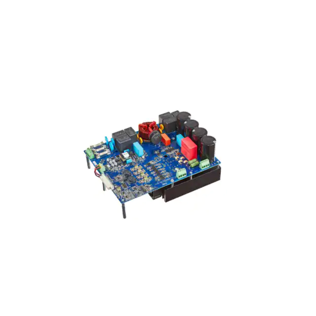
The next two figures illustrate the functional groups on the top and bottom side of the evaluation board. The
functional groups are explained in Table 3.
Figure 2
Top view of the Eval-M5-E1B1245N-SiC
Application Note - AN2019-25
7
�CoolSiC™ MOSFET Motor Drives Evaluation Board for 7.5 kW
Eval-M5-E1B1245N-SiC
Design features
Figure 3
Table 3
Side view of the Eval-M5-E1B1245N-SiC
Functional groups of Eval-M5-E1B1245N-SiC
Nr.
Functional groups
1
AC input connector with fuses
2
Varistors for overvoltage protection
3
EMI filter
4
Rectifier with precharge relay and precharge NTC resistors
5
DC-bus capacitors, balancing resistors and DC-bus connector
6
Power module FS45MR12W1M1_B11 with phase current shunts
7
High-side MOSFET drivers with -DACs for shunt sensors
8
Low-pass filter of -signals and overcurrent comparators
9
Connector for controller
10
Isolated power supply for MOSFET drivers
11
DC-bus voltage measurement with -DAC
12
Low-side MOSFET drivers
13
Flyback converter for auxiliary supply
14
Overcurrent detection and measuring shunt
15
Rectifier mounted on heatsink
16
Power module mounted on heatsink
17
Heatsink with fans
Application Note - AN2019-25
8
�CoolSiC™ MOSFET Motor Drives Evaluation Board for 7.5 kW
Eval-M5-E1B1245N-SiC
Design features
3.2
Pin assignment
General information about the connectors of the Eval-M5-E1B1245N-SiC evaluation board is reported.
Table 4 includes the details of the AC input connector X1.
Table 4
X1 – AC line connector
No.
Pin
Details
1
Line phase 1
2
Line phase 2
3
Line phase 3
4
EARTH
Table 5 provides the details of the motor side connector X2.
Table 5
X2 – Motor side connector
No.
Pin
Details
1
EARTH
Connect to X1/4 via heatsink
No connection without heatsink!
2
U
Connect to motor phase W
3
V
Connect to motor phase V
4
W
Connect to motor phase U
Table 6 provides the pin assignments of driver board connector X10. This connector is the interface to the
controller board.
Table 6
X10 – Power board connector
No.
Pin
Details
A1
-
-
A2
-
-
A3
-
-
A4
-
-
A5
-
-
A6
-
-
A7
-
-
A8
-
-
A9
-
-
A10
I_W
Phase W current sense output, scale 76.56 mV/A, offset 2.5 V
A11
I_V
Phase V current sense output, scale 76.56 mV/A, offset 2.5 V
A12
I_U
Phase U current sense output, scale 76.56 mV/A, offset 2.5 V
A13
-
-
A14
-
-
A15
-
-
A16
GND
Ground
Application Note - AN2019-25
9
�CoolSiC™ MOSFET Motor Drives Evaluation Board for 7.5 kW
Eval-M5-E1B1245N-SiC
Design features
No.
Pin
Details
B1
/ENABLE
/ENABLE signal – if high drivers are disabled
B2
/FAULT
/FAULT signal – active low when overcurrent or overtemperature is detected
B3
PWMWH
3.3 V compatible logic input for high-side gate driver-Phase W
B4
PWMWL
3.3 V compatible logic input for low-side gate driver-Phase W
B5
PWMVH
3.3 V compatible logic input for high-side gate driver-Phase V
B6
PWMVL
3.3 V compatible logic input for low-side gate driver-Phase V
B7
PWMUH
3.3 V compatible logic input for high-side gate driver-Phase U
B8
PWMUL
3.3 V compatible logic input for low-side gate driver-Phase U
B9
-
-
B10
-
-
B11
-
-
B12
-
-
B13
DCBsense
DC bus voltage sense output, scale 5 mV/V (1/200)
B14
VTH
Thermistor voltage output, 100°C = 0.448 V
B15
-
-
B16
VCC
On board 5 V supply, max. 120 mA
Table 7 denotes the details of the fan connector X4. The connector is provided for two fans with a nominal voltage
of 12 V cooling the heatsink. The maximum output current is limited to 180 mA. The connector is connected via
two series resistors to a supply of 15 V. Consequently, it is possible to drive most fans with a nominal voltage of
12 V in the power range of 0.6 W to 1 W in their allowed voltage range.
Table 7
X4 – DC bus connector
S. No. Pin
Details
1
Fan1-
Connected via 8.2 Ω resistor to -15 V, max. 180 mA
2
Fan1*
Connected via 8.2 Ω resistor to GND, max. 180 mA
3
Fan2-
Connected to Fan1-
4
Fan2+
Connected to Fan1+
Table 8 includes the details of the DC bus connector X6.
Table 8
X6 – DC bus connector
S. No.
Pin
Details
1
DC+
Connected to positive side of DC-bus capacitor
2
DC M
3
DC- M
Connected to midpoint of DC-bus capacitor
Do not connect load at this point!
4
DC-
Connected to negative side of DC-bus capacitor
Application Note - AN2019-25
10
�CoolSiC™ MOSFET Motor Drives Evaluation Board for 7.5 kW
Eval-M5-E1B1245N-SiC
Design features
The following table provides the details of the X7 digital measurement connector.
Table 9
X7 – measurement connector
S. No.
Pin
Details
1
Clock_Iu
20 MHz clock output, signal level 5 V
2
GND
3
DS_Iu
4
GND
5
Clock_Iv
6
GND
7
DS_Iv
8
GND
9
Clock_Iw
10
GND
11
DS_Iw
12
GND
13
Clock_Vdc
14
GND
15
DS_Vdc
16
GND
Application Note - AN2019-25
modulated output of current measurement, phase U,
signal level 5 V,
50% positive equals 0 A, 89.06% positive equals +25 A, 10.94% positive
equals -25 A
20 MHz clock output, signal level 5 V
modulated output of current measurement, phase V,
signal level 5 V,
50% positive equals 0 A, 89.06% positive equals +25 A, 10.94% positive
equals -25 A
20 MHz clock output, signal level 5 V
modulated output of current measurement, phase W,
signal level 5 V,
50% positive equals 0 A, 89.06% positive equals +25 A, 10.94% positive
equals -25 A
20 MHz clock output, signal level 5 V
modulated output of DC link voltage measurement,
signal level 5 V,
50% positive equals 0 V, 89.06% positive equals 851 V
11
�CoolSiC™ MOSFET Motor Drives Evaluation Board for 7.5 kW
Eval-M5-E1B1245N-SiC
Design features
3.3
Analogue measurement adjustment
In order to achieve a precise measurement of the output currents and a symmetric overcurrent detection, the
offset voltage of the analogue signals must be adjusted. All relevant parts for the adjustment of the offset voltage
are shown in Figure 4.
Figure 4
Relevant parts for offset adjustments
The DC-bus voltage measurement has only a small deviation; consequently, there is no offset compensation
necessary.
To adjust the current offset, simply vary R554 at no load until either the software readings of the currents are zero
or the voltages at the currents’ test points reach almost 2.5 V. Due to component tolerances, an exact adjustment
of all three currents to zero at the same time will not be possible.
Additional information about the circuit itself can be found in the chapter “Digital to analogue converter”.
Application Note - AN2019-25
12
�CoolSiC™ MOSFET Motor Drives Evaluation Board for 7.5 kW
Eval-M5-E1B1245N-SiC
Schematics and layout
4
Schematics and layout
4.1
Overview
An overview of the board’s schematics is given in Figure 5. Basically, the schematic can be divided into four
subcategories: the input circuit of the converter, the auxiliary supply, the power stage and the measurements.
The external controller board has to be connected to the evaluation board by the X10 driver board connector.
The logical ground is connected to earth by the resistors R12 to R14.
Figure 5
4.2
Overview and driver board connector
Input circuit
The input circuit is shown in Figure 6. It is equipped with two NTC resistors which limit the inrush current. The
resistors are bypassed after the start of the auxiliary supply and a constant delay time. The DC-bus consists of
four electrolytic capacitors and one film capacitor as well as four ceramic capacitors for the high-frequency ripple
currents. The electrolytic capacitors are series-connected and balanced with two resistors.
Application Note - AN2019-25
13
�CoolSiC™ MOSFET Motor Drives Evaluation Board for 7.5 kW
Eval-M5-E1B1245N-SiC
Schematics and layout
Figure 6
4.3
Mains input and precharge circuit
EMI filter
The Eval-M5-E1B1245N-SiC is equipped with an EMI filter circuit to present a complete solution. Please note that
the board is not qualified for connection to public grids. A laboratory power supply, an isolation transformer or
any other isolation device is required. The circuit is depicted in Figure 7.
Figure 7
EMI filter
The EMI filter is designed to minimize high-frequency emissions to the connected grid. Lower harmonics of the
grid current are not suppressed. An additional mains line choke must be used to fulfil harmonic standards. In
addition, a mains line choke reduces the crest factor of the input current. Hence, an external choke allows higher
rms input currents leading to a higher output power. Without an additional mains line choke, an output power
of approx. 6 kW can be achieved at 400 V line voltage.
However, the conducted EMI emission strongly depends on several operating conditions like the connected
motor, used switching frequency, etc. Consequently, the implemented filter does not necessarily meet the
required standard. If necessary, a Vacuumschmelze W 424-53 ring core, or similar, with three turns, can be added
to the supply lines as a common mode choke to further reduce the conducted EMI.
Application Note - AN2019-25
14
�CoolSiC™ MOSFET Motor Drives Evaluation Board for 7.5 kW
Eval-M5-E1B1245N-SiC
Schematics and layout
4.4
Auxiliary supply
All supply voltages are generated by a flyback converter, supplied from the DC-bus. It starts operation at a bus
voltage of 477 Vdc, which corresponds to approximately 340 Vac input voltage. The supply circuit is implemented
with an Infineon ICE5QSAG control IC. The supply voltages are isolated from the DC-bus potential by a basic
insulation. The complete schematic is shown in Figure 8.
Figure 8
Auxiliary supply
The flyback converter generates three voltages. The auxiliary winding on the primary side of the transformer
generates an unregulated 17.6 V supply for the control IC itself. On the transformer’s secondary side, two output
voltages are generated: a regulated 15 V and indirect regulated +6 V. The 15 V supply voltage is mainly used for
the MOSFET driver supply circuit. From this voltage, a -5 V supply voltage is derived by a linear regulator used for
the negative supply for the analogue circuitry of the board. The positive analogue supply is directly connected to
the +6 V supply. This voltage rail is also used to generate the +5 V for the controller and overcurrent threshold
generations.
If the Eval-M5-E1B1245N-SiC is to be used with low DC-bus voltages below the start-up threshold of the flyback
converter, it is possible to supply it with an external power supply. Therefore the test points TP651, TP656 and
TP661 can be used. These test points are labelled with their corresponding voltage on the PCB. The points are
depicted in Figure 9.
Application Note - AN2019-25
15
�CoolSiC™ MOSFET Motor Drives Evaluation Board for 7.5 kW
Eval-M5-E1B1245N-SiC
Schematics and layout
Figure 9
4.5
Major power supply test points
Power stage
The schematic of the power stage is shown in Figure 10. The three-phase legs of the sixpack power module
FS45R12M1W1_B11 are connected to one film capacitor and four ceramic capacitors. Two of the ceramic
capacitors are connected directly to the power module in front of the current measuring shunt. For the film
capacitors, two alternate packages can be mounted. Both high-frequency capacitor types are placed as close as
possible to the power module to minimize overvoltage at switching. Only two of the ceramic capacitors are
connected in front of the shunt to limit short-circuit energy. The DC-bus is led through to the X6 connector.
The current measuring shunt is used to detect output short-circuits. An overcurrent protection circuit is used to
monitor the shunt voltage and to disable all switches in overcurrent condition.
At each phase the output current is measured by a shunt resistor. The shunt voltages are measured by galvanic
isolated -DACs. Their supply is derived from an additional voltage level of the top-side driver supply circuit.
The voltage of the DC-bus is measured by a voltage divider and the same isolated -DAC supplied from an
additional driver voltage of the low-side driver supply. The functionalities of these blocks are explained below.
The NTC of the power module is used for generating a temperature-related measuring voltage Vth.
Figure 10
Power stage
Application Note - AN2019-25
16
�CoolSiC™ MOSFET Motor Drives Evaluation Board for 7.5 kW
Eval-M5-E1B1245N-SiC
Schematics and layout
4.6
Driver circuit
Each of the six MOSFETS is driven by Infineon’s MOSFET EiceDRIVER 1EDI20H12AH without any special circuitry
at the output. The positive input is protected by an additional glitch filter and a pull-down resistor. All negative
inputs are connected together and are used for a global /ENABLE signal. The circuit which is used for each phase
leg is shown in Figure 11.
Figure 11
Driver circuit for one-phase leg
Figure 12
Driver power supply
Application Note - AN2019-25
17
�CoolSiC™ MOSFET Motor Drives Evaluation Board for 7.5 kW
Eval-M5-E1B1245N-SiC
Schematics and layout
The rectifier circuit generates three voltage levels for each driver: a regulated negative voltage for safely turning
off the power MOSFET, +15 V for turning on the power MOSFET, and additionally +5 V for the additional current
and voltage measurement. The circuit is shown in Figure 13.
Figure 13
Rectifier circuit of driver power supply
The regulated negative voltage can be adjusted in eight steps by placing jumpers on the X8 pin header. This
adjustment must be done for each rectifier circuit separately. By placing the jumpers in this way, the feedback
resistor of the negative voltage regulator is changed. Consequently, its output voltage can be adjusted. The
selectable voltages are shown in Table 10.
Additionally, it is possible to use real 0 V turn-off voltage if R10 is removed and TP1 is connected to TP5. Be careful
when adjusting the negative voltage! Load conditions might occur which could lead to the undesired turn-on of
the power switches.
The jumpers must not be changed under switching conditions.
Table 10
X8 pin header negative gate voltage selection
Jumper setting
Negative gate voltage
-5.6 V
-4.9 V
-4.2 V
-3.5 V
-2.8 V
Application Note - AN2019-25
18
�CoolSiC™ MOSFET Motor Drives Evaluation Board for 7.5 kW
Eval-M5-E1B1245N-SiC
Schematics and layout
Jumper setting
Negative gate voltage
-2.0 V
-1.3 V
-0.6 V
4.7
Thermistor output
The temperature of the power module is measured with the module-integrated NTC resistor. The NTC resistor is
connected to 5 V via a series resistor of 10 kΩ. The resulting NTC voltage is fed to the control board via an amplifier
with a voltage gain of two. If necessary, the signal level can be changed by exchanging the resistors R617, R620,
R621 and R623. The evaluation circuit is depicted in Figure 14.
Figure 14
Evaluation circuit for NTC measurement
The dependency of the generated output voltage vs. the power module temperature is shown in Figure 15.
Application Note - AN2019-25
19
�CoolSiC™ MOSFET Motor Drives Evaluation Board for 7.5 kW
Eval-M5-E1B1245N-SiC
Schematics and layout
Figure 15
4.8
Power module temperature output
Current measurement
The three-phase currents are measured by shunt resistors. Each shunt voltage is measured by a galvanically
isolated -modulator. The modulator generates a -modulated bitstream output with a clock frequency of
20 MHz. The circuit can be seen in Figure 16. The modulator is supplied via the +5 V output from the rectifier
circuit.
Figure 16
4.9
Phase-current measurement
Voltage measurement
Similar to the current measurement, the DC-bus voltage is measured via a voltage divider and the galvanically
isolated -modulator. The circuit can be seen in Figure 17.
Application Note - AN2019-25
20
�CoolSiC™ MOSFET Motor Drives Evaluation Board for 7.5 kW
Eval-M5-E1B1245N-SiC
Schematics and layout
Figure 17
DC-bus voltage measurement
Application Note - AN2019-25
21
�CoolSiC™ MOSFET Motor Drives Evaluation Board for 7.5 kW
Eval-M5-E1B1245N-SiC
Schematics and layout
4.10
Digital-to-analogue converter
The evaluation board contains four discrete digital-to-analogue converters to generate analogue signals from
the digital -modulated bit streams. The analogue signals are used for the on-board protection as well as for
the external controller. The conversion is done by second-order low pass filters with approximately 6.5 kHz
bandwidth. The circuit is shown in Figure 18. At zero input, the -converter generates a bitstream with 50% duty
cycle. For offset adjustment, the reference voltage of the low pass filters can be adjusted via the R5564
potentiometer for all three currents.
The four -modulated bitstreams can be measured directly at the X7 pin headers.
Figure 18
Measurement digital-to-analogue conversion
The Eval-M5-E1B1245N-SiC evaluation board is equipped with an overcurrent and overtemperature protection.
If an overcurrent or overtemperature event is detected, the /FAULT signal is pulled low and the MOSFET drivers
are simultaneously disabled for around 30 ms. The circuit is depicted in Figure 19.
Application Note - AN2019-25
22
�CoolSiC™ MOSFET Motor Drives Evaluation Board for 7.5 kW
Eval-M5-E1B1245N-SiC
Schematics and layout
Figure 19
Protection circuit and temperature measurement
The overcurrent detection is provided with six ultra-low forward-voltage drop diodes (D600 … D605) which
rectify the peak current of each phase. The peak positive value and the peak negative value are compared with a
threshold value. If one value is exceeded, the /FAULT signal is triggered.
The overtemperature detection directly monitors the NTC voltage. A voltage below 0.224 V triggers the /FAULT
signal. This threshold corresponds to a measured temperature of 100°C.
4.11
Overcurrent / Short-circuit protection
The circuit which monitors the voltage across a 3 mΩ shunt placed in the DC-path of the power module is
shown in Figure 20. A low-side driver with an overcurrent protection feature is used here. The driver stage itself
is unused. The Infineon 1ED44176N01F has 0.5 V overcurrent trigger threshold. This leads to a nominal current
threshold of 167 A.
Figure 20
Short-circuit protection
Application Note - AN2019-25
23
�CoolSiC™ MOSFET Motor Drives Evaluation Board for 7.5 kW
Eval-M5-E1B1245N-SiC
Schematics and layout
A low pass filter (R61/C63) is placed at the OCP pin of the IC. Its time constant of 484 ns is required to block high
voltage spikes at fast current rises due to the parasitic inductance of the measuring shunt and its connection.
If an overcurrent is detected, the EN/FAULT pin of the driver is pulled low and the LED of the connected
optocoupler turns on. Hence, the isolated side of the optocoupler turns low and the /FAULT signal is pulled low.
Consequently, all MOSFET drivers are turned off. The overall time delay from overcurrent to MOSFET gate low is
approximately 1 µs.
The circuit is supplied via the low-side gate driver supply. This supply is referenced to the source of the low-side
MOSFETs which is in front of the shunt. Consequently, the supply of the OCP protection is decoupled with a diode
(D61) and buffered with a capacitor (C64). This leads to a voltage drop of approximately 1 V in overcurrent
condition, however, this is still sufficient to supply the circuit.
4.12
PCB layout
The layout of this board is especially designed for evaluation purposes. Consequently, it has several test points
and is not necessarily suited for continuous operation at full load. The PCB has four electrical layers with 35 µm
copper. The size is 204 mm x 259 mm. The PCB thickness is 1.6 mm. For more details on the layout design and
the latest Gerber-files, contact our technical support team.
Figure 21 and Figure 22. show the top and bottom assembly of the evaluation board, respectively.
Figure 21
Top assembly print of the Eval-M5-E1B1245N-SiC evaluation board
Application Note - AN2019-25
24
�CoolSiC™ MOSFET Motor Drives Evaluation Board for 7.5 kW
Eval-M5-E1B1245N-SiC
Schematics and layout
Figure 22
Bottom assembly print of the Eval-M5-E1B1245N-SiC evaluation board
Application Note - AN2019-25
25
�CoolSiC™ MOSFET Motor Drives Evaluation Board for 7.5 kW
Eval-M5-E1B1245N-SiC
Bill of material
5
Bill of material
Table 11
No.
Bill of material
Qty. Part description
Designator
Part number
Manufacturer
1
11
SCREW M3: ZYK ISK / 6mm /
ST8,8 vz bp
SCREW1, SCREW2,
SCREW3, SCREW4,
SCREW5, SCREW6,
SCREW7, SCREW8,
SCREW9, SCREW10,
SCREW11
2
1
SCREW M4: ZYK ISK / 10mm /
ST8,8 vz bp
SCREW16
3
4
SCREW M4: ZYK ISK / 25mm /
ST8,8 vz bp
SCREW12, SCREW13,
SCREW14, SCREW15
4
2
SCREW M5: ZYK ISK / 20mm /
ST8,8 vz bp
SCREW17, SCREW18
5
2
WASHER: 4,3mm / ST vz bp
WASHER1, WASHER2
6
1
WASHER: 5,3mm / ST vz bp
WASHER3
7
2
SCREW LOCK: M4 / Tellerform
gerippt / ST vn
BOLTLOCK1,
BOLTLOCK2
8
1
SCREW LOCK: M5 / Tellerform
gerippt / ST vn
BOLTLOCK3
05.13.121
ETTINGER GmbH
Disrelec
9
11
SPACER BOLT: M3 / M3 / 12mm /
STvz / SW 5,5mm / Freistich
SPACER1, SPACER2,
SPACER3, SPACER4,
SPACER5, SPACER6,
SPACER7, SPACER8,
SPACER9, SPACER10,
SPACER11
10
4
SPACER BOLT: M3 / M3 / 40mm /
STvz / SW 6mm
SPACER12, SPACER13,
SPACER14, SPACER15
DISTIN3060S-40
11
1
DIODE ZENER: BZV55-C18
D62
BZV55-C18
12
1
DIODE ZENER: BZV55-B22
D653
BZV55-B22
13
2
DIODE ZENER: BZX84-C5V6
D655, D658
BZX84-C5V6
BAT165
14
27
DIODE SCHOTTKY: BAT165
D60, D61, D100, D101,
D200, D400, D657,
R1.D1, R1.D2, R1.D3,
R1.D4, R1.D6, R2.D1,
R2.D2, R2.D3, R2.D4,
R2.D6, R3.D1, R3.D2,
R3.D3, R3.D4, R3.D6,
R4.D1, R4.D2, R4.D3,
R4.D4, R4.D6
15
6
DIODE SCHOTTKY: BAT60A
D600, D601, D602, D603, BAT60AE6327HT
D604, D605
SA1
Application Note - AN2019-25
26
Infineon
Infineon
�CoolSiC™ MOSFET Motor Drives Evaluation Board for 7.5 kW
Eval-M5-E1B1245N-SiC
Bill of material
No.
Qty. Part description
Designator
Part number
16
4
DIODE STANDARD: 1N4148WS
R1.D5, R2.D5, R3.D5,
R4.D5
1N4148WS
17
2
DIODE STANDARD: EGL34D-E3
D652, D656
EGL34D-E3
Vishay
18
1
DIODE STANDARD: CMR1U-13M
D651
CMR1U-13M
Central
Semiconductor
Corp.
19
2
DIODE STANDARD: MURS320T3G
D650, D654
MURS320T3G
ON
Semiconductor
20
1
RECT BRIDGE: SBR2512W
GL400
SBR2512W
Multicomp
21
4
IC ADC: AMC1303M0520
CU.IC300, CV.IC300,
CW.IC300, IC350
AMC1303M0520
Texas
Instruments
22
3
IC OPAMP: LM7322MA
U550, U551, U552
LM7322MA
Texas
Instruments
23
1
IC OPAMP: LM7321MF
U602
LM7321MF
Texas
Instruments
24
1
IC DRIVER: IR2085
U200
IR2085S
International
Rectifier
25
6
IC DRIVER: 1EDI20H12AH
U.U150, U.U151, V.U150,
1EDI20H12AH
V.U151, W.U150, W.U151
Infineon
26
1
IC DRIVER: 1ED44176N01F
U61
1ED44176N01F
Infineon
27
1
IC VOLT REG: TL431AFDT
U653
TL431AFDT
NXP
28
1
IC PWM REG: ICE5QSAG
U652
ICE5QSAG
Infineon
29
1
IC VOLT REG: IFX1117ME V
U650
IFX1117ME V
Infineon
30
4
IC VOLT REG:
IFX20001MBV50HTSA1
R1.U1, R2.U1, R3.U1,
R4.U1
IFX20001MBV50H
Infineon
TSA1
31
4
IC VOLT REG: TPS72301DBVTG4
R1.U3, R2.U3, R3.U3,
R4.U3
TPS72301DBVTG Texas
4
Instruments
32
2
IC COMPARATOR: LM393D
U600, U601
LM393D
Texas
Instruments
33
1
IC LOGIC: 74HCT7541D
U20
74HCT7541D
NXP
34
1
IC OPTOCOUPLE: SFH6156-4T
U651
SFH6156-4T
Vishay
35
1
IC OPTOCOUPLE: TLP2748
U60
TLP2748
Toshiba
36
7
LED: SMD / 0805 / gn
LED10, LED650, LED651,
R1.LED1, R2.LED1,
SMD-G0805-02
R3.LED1, R4.LED1
Sloan AG
37
3
TRANS NPN: BC847C
Q10, Q100, Q400
BC847C
Infineon
38
1
TRANS PNP: BC857C
Q651
BC857C
Infineon
39
2
MOSFET: BSL302SN
Q200, Q201
BSL302SN
Infineon
40
1
MOSFET: 2SK4177
Q650
2SK4177
ON
Semiconductor
41
1
MOSFET-MODULE Easy 1b
M50
FS45MR12W1M1_
Infineon
B11
Application Note - AN2019-25
27
Manufacturer
�CoolSiC™ MOSFET Motor Drives Evaluation Board for 7.5 kW
Eval-M5-E1B1245N-SiC
Bill of material
No.
Qty. Part description
Designator
42
6
RES SMD 0805: 0R0 / 1% / 0,125W
R11, R555, R556, R611,
R617, R653
43
1
RES SMD 0805: 2R2 / 1% / 0,125W R200
44
4
RES SMD 0805: 3R3 / 1% / 0,125W
45
24
R62, R101, R201, R203,
R357, R667, U.R150,
U.R151, U.R152, U.R156,
U.R157, U.R158, V.R150,
RES SMD 0805: 10R / 1% / 0,125W V.R151, V.R152, V.R156,
V.R157, V.R158, W.R150,
W.R151, W.R152,
W.R156, W.R157,
W.R158
46
1
RES SMD 0805: 20R / 1% / 0,125W R356
47
6
CU.R301, CU.R303,
RES SMD 0805: 22R / 1% / 0,125W CV.R301, CV.R303,
CW.R301, CW.R303
48
2
RES SMD 0805: 27R / 1% / 0,125W R662, R663
49
11
RES SMD 0805: 100R / 1% /
0,125W
R500, R501, R502, R503,
R601, R602, R603, R604,
R605, R606, R618
50
1
RES SMD 0805: 680R / 1% /
0,125W
R614
51
6
RES SMD 0805: 1k0 / 1% / 0,125W
R16, R100, R204, R607,
R609, R622
52
2
RES SMD 0805: 1k2 / 1% / 0,125W R674, R676
53
2
RES SMD 0805: 1k3 / 1% / 0,125W R610, R624
54
1
RES SMD 0805: 2k2 / 1% / 0,125W R60
55
2
RES SMD 0805: 2k7 / 1% / 0,125W R15, R677
56
2
RES SMD 0805: 3k3 / 1% / 0,125W R405, R669
57
2
RES SMD 0805: 4k7 / 1% / 0,125W R17, R61
58
3
RES SMD 0805: 5k6 / 1% / 0,125W R567, R572, R652
59
1
RES SMD 0805: 6k8 / 1% / 0,125W R678
60
1
RES SMD 0805: 8k2 / 1% / 0,125W R670
61
13
R102, R613, R615, R619,
R621, R623, R680,
RES SMD 0805: 10k / 1% / 0,125W
U.R153, U.R159, V.R153,
V.R159, W.R153, W.R159
62
2
RES SMD 0805: 13k / 1% / 0,125W R570, R571
63
1
RES SMD 0805: 15k / 1% / 0,125W R666
64
1
RES SMD 0805: 22k / 1% / 0,125W R616
Application Note - AN2019-25
Part number
Manufacturer
R1.R4, R2.R4, R3.R4,
R4.R4
28
�CoolSiC™ MOSFET Motor Drives Evaluation Board for 7.5 kW
Eval-M5-E1B1245N-SiC
Bill of material
No.
Qty. Part description
Designator
Part number
Manufacturer
65
6
RES SMD 0805: 27k / 1% / 0,125W
R550, R551, R558, R559,
R562, R563
66
5
RES SMD 0805: 33k / 1% / 0,125W
R1.R2, R2.R2, R3.R2,
R4.R2, R661
67
1
RES SMD 0805: 39k / 1% / 0,125W R573
68
1
RES SMD 0805: 47k / 1% / 0,125W R675
69
3
RES SMD 0805: 56k / 1% / 0,125W R552, R560, R564
70
1
RES SMD 0805: 68k / 1% / 0,125W R202
71
1
RES SMD 0805: 220k / 1% /
0,125W
R612
72
6
RES SMD 0805: 10k / 0,1% /
0,125W
R553, R557, R565, R569,
R600, R608
73
1
RES SMD 0805: 14k / 0,1% /
0,125W
R668
74
9
RES SMD 0805: 0R15 / 1% /
0,125W
R1.R1, R1.R10, R2.R1,
R2.R10, R3.R1, R3.R10,
R4.R1, R4.R10, R205
75
2
RES SMD 1206: 22R / 1% / 0,25W
R658, R664
76
1
RES SMD 1206: 82R / 1% / 0,25W
R404
77
3
RES SMD 1206: 1k0 / 1% / 0,25W
R681, R682, R683
78
1
RES SMD 1206: 2k2 / 1% / 0,25W
R679
79
1
RES SMD Melf: 2R2 / 1% / 0,4W
R673
80
2
RES THT: PO591-0 5T 56K
R400, R401
PO591-0 5T 56K
VITROHM
81
3
VARISTOR: 510V RMS 20MM MOVR453, R454, R455
20D821K
MOV-20D821K
Bourns
82
2
RES NTC: SL32 5R020
R402, R403
SL32 5R020
Ametherm
83
1
RES VAR: 1k / 250mW / SMD
R554
23BR1KLFTR
BI Technologies
84
5
RES SMD 2512: 68k / 1% / 1W
R350, R351, R352, R353,
R354
85
3
RES SMD 2512: 0R0 / 1W
R12, R13, R14
86
2
RES SMD 2512: 8R2 / 1% / 3W
R684, R685
35228R2JT
TE Connectivity
87
2
RES SMD 2512: 10k / 1% / 1W
R651, R655
88
3
RES SMD 2512: 220k / 1% / 2W
R450, R451, R452
89
3
RES SMD 2512: 0R002 / 1% / 3W
CU.R302, CV.R302,
CW.R302
CRE2512-FZR002E-3
Bourns
90
4
RES SMD 0603: 8k2 / 1% / 0,1W
R1.R5, R2.R5, R3.R5,
R4.R5
RES SMD 0603: 10k / 1% / 0,1W
R1.R3, R1.R7, R1.R8,
R1.R9, R2.R3, R2.R7,
R2.R8, R2.R9, R3.R3,
R3.R7, R3.R8, R3.R9,
R4.R3, R4.R7, R4.R8,
91
22
Application Note - AN2019-25
29
�CoolSiC™ MOSFET Motor Drives Evaluation Board for 7.5 kW
Eval-M5-E1B1245N-SiC
Bill of material
No.
Qty. Part description
Designator
R4.R9, R20, R21, R22,
R23, R24, R25
92
4
RES SMD 0603: 20k / 1% / 0,1W
R1.R6, R2.R6, R3.R6,
R4.R6
93
3
RES SMD 2010: 10M / 1% / 0,75W
R650, R654, R659
94
3
RES SMD 2010: 3M3 / 5% / 0,75W
R656, R660, R665
95
1
RES SMD: 0R003 / 1% / 5W
R50
96
1
CAP CER 0805: 47p / 50V / X7R
C100
97
8
CAP CER 0805: 100p / 50V / X7R
C206, C666, U.C150,
U.C155, V.C150, V.C155,
W.C150, W.C155
98
5
CAP CER 0805: 220p / 50V / X7R
C63, C550, C552, C556,
C558
99
6
CAP CER 0805: 470p / 50V / X7R
C600, C601, C602, C606,
C607, C608
100
3
CAP CER 0805: 680p / 50V / X7R
C551, C555, C557
101
4
CAP CER 0805: 1n / 50V / X7R
C207, C665, C671, C678
102
1
CAP CER 0805: 2n2 / 50V / X7R
C561
103
4
CAP CER 0805: 4n7 / 50V / X7R
C354, CU.C304, CV.C304,
CW.C304
104
1
CAP CER 0805: 6n8 / 50V / X7R
C676
105
4
CAP CER 0805: 10n / 50V / X7R
C500, C501, C502, C503
106
30
CAP CER 0805: 100n / 50V / X7R
C20, C60, C61, C200,
C351, C353, C563, C564,
C565, C603, C604, C605,
C610, C611, C612, C613,
C662, C670, CU.C301,
CU.C303, CV.C301,
CV.C303, CW.C301,
CW.C303, U.C152,
U.C157, V.C152, V.C157,
W.C152, W.C157
107
1
CAP CER 0805: 680n / 50V / X7R
C672
108
1
CAP CER 0805: 1u / 50V / X7R
C62
109
2
CAP CER 0805: 2u2 / 50V / X7R
C554, C559
CAP CER 0805: 4u7 / 35V / X5R
C64, C201, C202, C203,
C204, C205, C350, C352,
C405, C406, C562, C609,
C654, C658, C661, C668,
C669, C674, C675,
CU.C300, CU.C302,
CV.C300, CV.C302,
CW.C300, CW.C302,
110
57
Application Note - AN2019-25
30
Part number
Manufacturer
CSS2H-3920K3L00F
Bourns
�CoolSiC™ MOSFET Motor Drives Evaluation Board for 7.5 kW
Eval-M5-E1B1245N-SiC
Bill of material
No.
Qty. Part description
Designator
Part number
R1.C1, R1.C2, R1.C3,
R1.C4, R1.C5, R2.C1,
R2.C2, R2.C3, R2.C4,
R2.C5, R3.C1, R3.C2,
R3.C3, R3.C4, R3.C5,
R4.C1, R4.C2, R4.C3,
R4.C4, R4.C5, U.C151,
U.C153, U.C156, U.C158,
V.C151, V.C153, V.C156,
V.C158, W.C151,
W.C153, W.C156,
W.C158
Manufacturer
111
1
CAP CER 0805: 18p / 50V / X7R
C659
112
2
CAP CER 1206: 470p / 200V / X7R
C651, C655
113
6
CAP CER: VY1472M61Y5UC63V0
CY450, CY451, CY452,
CY453, CY454, CY455
VY1472M61Y5UC
63V0
114
4
CAP CER: 47n / 1,5kV / X7R
C50, C51, C54, C55
2220SC473KAT1A AVX
115
1
CAP FILM: B32021A3102M
C664
B32021A3102M28
TDK
9
116
1
CAP FILM: B32021A3222M189
C650
B32021A3222M18
TDK
9
117
6
CAP FILM: 1u / 480V / X1
CX450, CX451, CX452,
CX453, CX454, CX455
F339X151048KKI
2B0
Vishay
118
1
CAP FILM: MKP 20u 800VDC DCLink 4Pin
C52
DCP4L052007GD
4K*SD
WIMA
119
2
CAP FILM: B32674D1105K000
C402, C677
B32674D1105K00
TDK
0
120
1
CAP ALUM: NACZ100M50V6,3X6,3 C660
121
6
CAP ALUM: 16SVPF180M
C652, C653, C656, C657,
16SVPF180M
C667, C673
122
4
CAP ALUM: 1200u/400V
C400, C401, C403, C404
Vishay
NACZ100M50V6.3
NIC Components
X6.3
Panasonic
B43630A9128M00
TDK
0
123
16
CAP CER 0603: 2u2 / 16V / X5R
R1.C8, R1.C9, R1.C10,
R1.C11, R2.C8, R2.C9,
R2.C10, R2.C11, R3.C8,
R3.C9, R3.C10, R3.C11,
R4.C8, R4.C9, R4.C10,
R4.C11
124
1
IND CM MODE: 744227
L200
744227
Würth Elektronik
125
2
IND CM MODE: 744221
L650, L651
744221
Würth Elektronik
126
1
IND CM MODE: T60405-S6123X317
L452
T60405-S6123X317
VACUUMSCHMEL
ZE
127
2
TRANSFORMER: T60403-F5046X007
TR200, TR201
T60403-F5046X007
VACUUMSCHMEL
ZE
Application Note - AN2019-25
31
�CoolSiC™ MOSFET Motor Drives Evaluation Board for 7.5 kW
Eval-M5-E1B1245N-SiC
Bill of material
No.
Qty. Part description
Designator
Part number
Manufacturer
128
3
FUSE: D6,3x32mm / 16A
F400, F401, F402
129
6
FUSE CLIP: 6,3mm
X401, X402, X403, X404,
X405, X406
80.400.001
Schurter
130
1
RELAY: RTS3L012
K400
1-1415898-9
TE Connectivity /
Schrack
131
1
CON MULTIPOLE: 2x16
X10
09 27 232 6801
Harting
132
5
CON: pinheader 2x3
R1.X8, R2.X8, R3.X8,
R4.X8, X11
826632-3
TE Connectivity
133
1
CON: pin header 2x8
X7
TSM-108-01-T-DV Samtec
134
3
CON TERM BLOCK: MKDS 3/ 45,08
X1, X2, X6
1712805
PHOENIX
CONTACT
135
1
CON TERM BLOCK: SPTA 1,5/ 43,81
X4
1751493
PHOENIX
CONTACT
136
2
FAN: EB40201S2-0000-999
FAN1, FAN2
EB40201S2-0000Sunon
999
137
1
TRANSFORMER: Flyback
T650
ÜP615694
Pikatron GmbH
138
1
HEATSINK: FISCHER_SK 85/150
HS1
SK 85/150 SA
Fischer
Elektronik
Application Note - AN2019-25
32
�CoolSiC™ MOSFET Motor Drives Evaluation Board for 7.5 kW
Eval-M5-E1B1245N-SiC
Measurements
6
Measurements
The following chapter provides some typical measurements made with the Eval-M5-E1B1245N-SiC evaluation
board. The board is supplied by a 400 V grid and is connected at the output to a symmetrical RL-load illustrated
in Figure 23.
Iac1
L
R
Iac2
L
R
Iac3
L
R
UR
Figure 23
Test load
The value of the inductance is 1.5 mH and the value of the resistor is 23 Ohm. With a nominal output current of
16 ARMS, the output power is about 5.9 kW. The switching frequency was set to 18 kHz. The following screenshot
shows the related measurement.
Figure 24
Measurement waveforms with test load
The output phase current (green) and the resistor voltage (red) are almost sinusoidal, whereas the input line
current (blue) shows the typical waveform of a capacitor charging current. Due to its high crest factor, the rmsvalue is as high as 15 A, even at only 6 kW input power. The yellow signal shows the rectified DC-bus voltage of
about 562 V.
Application Note - AN2019-25
33
�CoolSiC™ MOSFET Motor Drives Evaluation Board for 7.5 kW
Eval-M5-E1B1245N-SiC
Measurements
6.1
Thermal measurements
After the board was powered for over an hour at the above-mentioned load conditions, the following thermal
images were made. At the same time, the NTC temperature was measured with TModul ≈ 92 °C.
Figure 25
Thermal image of evaluation board at 18 kHz switching frequency
Figure 26
Thermal image of input area
Figure 27
Thermal image of power module area
Application Note - AN2019-25
34
�CoolSiC™ MOSFET Motor Drives Evaluation Board for 7.5 kW
Eval-M5-E1B1245N-SiC
Measurements
Figure 28
Thermal image of power module and rectifier (side view)
To evaluate the thermal behavior of the Eval-M5-E1B1245N-SiC evaluation board at 100 kHz switching frequency,
the current was reduced until the same module temperature of TModul ≈ 92 °C was measured. This point was
reached at 8 ARMS output current. Figure 29 shows the thermal image at this operating point.
Figure 29
6.2
Thermal image of evaluation board at 100 kHz switching frequency
EMI measurements
The conducted EMI emission of the evaluation board was measured according DIN EN 55011, connected to the
grid via a 32 A – LISN. In Figure 30, the emission and the threshold limits for industrial use (DIN EN 55011, class A,
group 1, ≤ 20 kVA) can be found. As one can see, the limits have almost been reached.
Application Note - AN2019-25
35
�CoolSiC™ MOSFET Motor Drives Evaluation Board for 7.5 kW
Eval-M5-E1B1245N-SiC
Measurements
Figure 30
Conducted EMI emission
The emissions can be damped under the limits by using a small external common mode choke. The next figure
shows the result using a Vacuumschmelze W 424-53 choke with three turns.
Figure 31
Conducted EMI emission with small external common mode choke
Application Note - AN2019-25
36
�CoolSiC™ MOSFET Motor Drives Evaluation Board for 7.5 kW
Eval-M5-E1B1245N-SiC
References
7
References
[1] Datasheet Infineon FS45MR12W1M1_B11
[2] Datasheet of Infineon Eice-Driver 1EDI20H12AH
[3] Datasheet of Texas Instruments isolated ΔΣ-Modulator AMC1303M2520
Application Note - AN2019-25
37
�CoolSiC™ MOSFET Motor Drives Evaluation Board for 7.5 kW
Eval-M5-E1B1245N-SiC
References
Revision History
Major changes since the last revision
Page or Reference
Description of change
1.0
Initial version
Application Note - AN2019-25
38
�Trademarks
All referenced product or service names and trademarks are the property of their respective owners.
Edition
ifx1owners.
Published by
Infineon Technologies AG
81726 Munich, Germany
© 2019 Infineon Technologies AG.
All Rights Reserved.
Do you have a question about this
document?
Email: erratum@infineon.com
Document reference
AppNote Number - AN2019-25
IMPORTANT NOTICE
The information contained in this application note is
given as a hint for the implementation of the product
only and shall in no event be regarded as a
description or warranty of a certain functionality,
condition or quality of the product. Before
implementation of the product, the recipient of this
application note must verify any function and other
technical information given herein in the real
application. Infineon Technologies hereby disclaims
any and all warranties and liabilities of any kind
(including without limitation warranties of noninfringement of intellectual property rights of any
third party) with respect to any and all information
given in this application note.
The data contained in this document is exclusively
intended for technically trained staff. It is the
responsibility of customer’s technical departments
to evaluate the suitability of the product for the
intended application and the completeness of the
product information given in this document with
respect to such application.
For further information on the product, technology,
delivery terms and conditions and prices please
contact your nearest Infineon Technologies office
(www.infineon.com).
WARNINGS
Due to technical requirements products may contain
dangerous substances. For information on the types
in question please contact your nearest Infineon
Technologies office.
Except as otherwise explicitly approved by Infineon
Technologies in a written document signed by
authorized
representatives
of
Infineon
Technologies, Infineon Technologies’ products may
not be used in any applications where a failure of the
product or any consequences of the use thereof can
reasonably be expected to result in personal injury.
�


 工商网监
湘ICP备2023018690号
工商网监
湘ICP备2023018690号
