PD -95037B
IRF7103PbF
l
l
l
l
l
l
l
l
Adavanced Process Technology
Ultra Low On-Resistance
Dual N-Channel MOSFET
Surface Mount
Available in Tape & Reel
Dynamic dv/dt Rating
Fast Switching
Lead-Free
HEXFET® Power MOSFET
S1
1
8
D1
G1
2
7
D1
S2
3
6
D2
G2
4
5
D2
VDSS = 50V
RDS(on) = 0.130Ω
ID = 3.0A
Top View
Description
The SO-8 has been modified through a customized
leadframe for enhanced thermal characteristics and
dual-die capability making it ideal in a variety of power
applications. With these improvements, multiple
devices can be used in an application with dramatically
reduced board space. The package is designed for
vapor phase, infra red, or wave soldering techniques.
Power dissipation of greater than 0.8W is possible in
a typical PCB mount application.
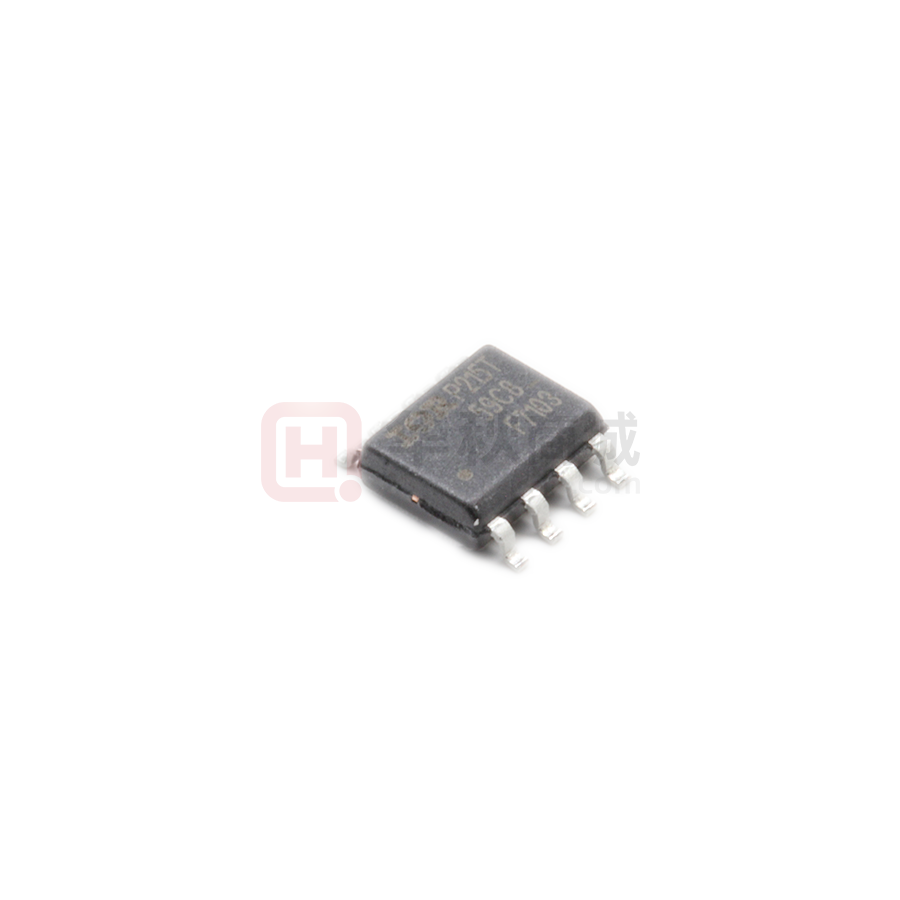
SO-8
Absolute Maximum Ratings
Parameter
ID @ TA = 25°C
ID @ TA = 70°C
IDM
PD @TA = 25°C
VGS
dv/dt
TJ, TSTG
Max.
Continuous Drain Current, VGS @ 10V
Continuous Drain Current, VGS @ 10V
Pulsed Drain Current
Power Dissipation
Linear Derating Factor
Gate-to-Source Voltage
Peak Diode Recovery dv/dt
Junction and Storage Temperature Range
Units
3.0
2.3
10
2.0
0.016
± 20
4.5
-55 to + 150
A
W
W/°C
V
V/nS
°C
Thermal Resistance Ratings
Parameter
RθJA
Maximum Junction-to-Ambient
Min.
Typ.
Max.
62.5
Units
°C/W
02/09/10
�IRF7103PbF
Electrical Characteristics @ TJ = 25°C (unless otherwise specified)
∆V(BR)DSS/∆TJ
Parameter
Drain-to-Source Breakdown Voltage
Breakdown Voltage Temp. Coefficient
Qg
Q gs
Qgd
td(on)
tr
td(off)
tf
Gate-to-Source Forward Leakage
Gate-to-Source Reverse Leakage
Total Gate Charge
Gate-to-Source Charge
Gate-to-Drain ("Miller") Charge
Turn-On Delay Time
Rise Time
Turn-Off Delay Time
Fall Time
Min.
50
1.0
Typ.
0.049
0.11
0.16
3.8
12
1.2
3.5
9.0
8.0
45
25
RDS(ON)
Static Drain-to-Source On-Resistance
VGS(th)
g fs
Gate Threshold Voltage
Forward Transconductance
IDSS
Drain-to-Source Leakage Current
LD
Internal Drain Inductance
4.0
LS
Internal Source Inductance
6.0
Ciss
Coss
Crss
Input Capacitance
Output Capacitance
Reverse Transfer Capacitance
290
140
37
V(BR)DSS
IGSS
Max. Units
Conditions
V
VGS = 0V, ID = 250µA
V/°C Reference to 25°C, ID = 1mA
0.13
VGS = 10V, ID = 3.0A
Ω
0.20
VGS = 4.5V, ID = 1.5A
3.0
V
VDS = VGS, ID = 250µA
S
VDS = 15V, ID = 3.0A
2.0
VDS = 40V, VGS = 0V
µA
25
VDS = 40V, VGS = 0V, T J = 55 °C
100
VGS = 20V
nA
-100
VGS = - 20V
30
ID = 2.0A
nC VDS = 25V
VGS = 10V
20
VDD = 25V
20
ID = 1.0A
ns
70
RG = 6.0Ω
50
RD = 25Ω
D
nH
pF
Between lead,6mm(0.25in.)
from package and center
of die contact
VGS = 0V
VDS = 25V
= 1.0MHz
G
Source-Drain Ratings and Characteristics
IS
I SM
V SD
t rr
Q rr
ton
Parameter
Continuous Source Current
(Body Diode)
Pulsed Source Current
(Body Diode)
Diode Forward Voltage
Reverse Recovery Time
Reverse RecoveryCharge
Forward Turn-On Time
Min. Typ. Max. Units
Conditions
D
MOSFET symbol
2.0
showing the
A
G
integral reverse
12
p-n junction diode.
S
1.2
V
TJ = 25°C, IS = 1.5A, V GS = 0V
70 100
ns
TJ = 25°C, IF = 1.5A
110 170
nC di/dt = 100A/µs
Intrinsic turn-on time is negligible (turn-on is dominated by LS+LD)
Notes:
Repetitive rating; pulse width limited by
Pulse width ≤ 300µs; duty cycle ≤ 2%.
ISD ≤ 1.8A, di/dt ≤ 90A/µs, VDD ≤ V(BR)DSS,
Surface mounted on FR-4 board, t ≤ 10sec.
max. junction temperature.
TJ ≤ 150°C
S
�IRF7103PbF
�C,
IRF7103PbF
�IRF7103PbF
V DS
VGS
RD
D.U.T.
RG
+
- VDD
10V
Pulse Width ≤ 1 µs
Duty Factor ≤ 0.1 %
Fig 10a. Switching Time Test Circuit
VDS
90%
TA, Ambient Temperature (°C)
10%
VGS
Fig 9. Maximum Drain Current Vs.
Ambient Temperature
td(on)
tr
t d(off)
tf
Fig 10b. Switching Time Waveforms
Thermal Response (Z thJA )
100
D = 0.50
0.20
10
0.10
0.05
0.02
1
0.1
0.0001
PDM
0.01
t1
SINGLE PULSE
(THERMAL RESPONSE)
t2
Notes:
1. Duty factor D = t 1 / t 2
2. Peak T J = P DM x Z thJA + TA
0.001
0.01
0.1
1
10
t1, Rectangular Pulse Duration (sec)
Fig 11. Maximum Effective Transient Thermal Impedance, Junction-to-Ambient
100
�IRF7103PbF
Current Regulator
Same Type as D.U.T.
QG
10V
QGS
50KΩ
.2µF
12V
.3µF
QGD
VG
D.U.T.
+
V
- DS
VGS
3mA
Charge
IG
ID
Current Sampling Resistors
Fig 12a. Basic Gate Charge Waveform
Fig 12b. Gate Charge Test Circuit
�IRF7103PbF
Peak Diode Recovery dv/dt Test Circuit
+
D.U.T
Circuit Layout Considerations
• Low Stray Inductance
• Ground Plane
• Low Leakage Inductance
Current Transformer
+
-
-
+
RG
•
•
•
•
Driver Gate Drive
P.W.
+
dv/dt controlled by R G
Driver same type as D.U.T.
ISD controlled by Duty Factor "D"
D.U.T. - Device Under Test
Period
D=
-
VDD
P.W.
Period
VGS=10V
D.U.T. ISD Waveform
Reverse
Recovery
Current
Body Diode Forward
Current
di/dt
D.U.T. VDS Waveform
Diode Recovery
dv/dt
Re-Applied
Voltage
Body Diode
VDD
Forward Drop
Inductor Curent
Ripple ≤ 5%
* VGS = 5V for Logic Level Devices
Fig 13. For N-Channel HEXFETS
ISD
*
�IRF7103PbF
SO-8 Package Outline(Mosfet & Fetky)
Dimensions are shown in milimeters (inches)
'
,1&+(6
0,1
0$;
$ ����� �����
$� ����� �����
E ����
����
F ����� �����
' ����
�����
( ����� �����
H
������%$6,&
H � ������%$6,&
+ ����� �����
. ����� �����
/ ����
����
��
\
��
',0
%
�
$
�
�
�
�
�
�
�
�
�
+
�����>����@�
(
$
�; H
H�
�;�E
�����>����@�
$
0,//,0(7(56
0,1
0$;
����
����
����
����
����
����
����
����
����
����
����
����
������%$6,&
�������%$6,&
����
����
����
����
����
����
��
��
.�[���
&
$�
\
�����>����@�
�;�F
�;�/
�
& $ %
)22735,17
�;������>����@
127(6�
����',0(16,21,1*� �72/(5$1&,1*�3(5�$60(�,1&+(6@�
����287/,1(�&21)2506�72�-('(&�287/,1(�06����$$�
����',0(16,21�'2(6�127�,1&/8'(�02/'�3527586,216�
�����02/'�3527586,216�127�72�(;&(('������>����@�
����',0(16,21�'2(6�127�,1&/8'(�02/'�3527586,216�
�����02/'�3527586,216�127�72�(;&(('������>����@�
����',0(16,21�,6�7+(�/(1*7+�2)�/($'�)25�62/'(5,1*�72
�����$�68%675$7(�
�����>����@
�;������>����@
SO-8 Part Marking Information
(;$03/(��7+,6�,6�$1�,5)������026)(7�
,17(51$7,21$/
5(&7,),(5
/2*2
;;;;
)����
�;������>����@
'$7(�&2'(��


 工商网监
湘ICP备2023018690号
工商网监
湘ICP备2023018690号
