IRFH7914PbF
HEXFET® Power MOSFET
Applications
l
l
Control MOSFET of Sync-Buck Converters
used for Notebook Processor Power
Control MOSFET for Isolated DC-DC
VDSS
30V
RDS(on) max
Qg
8.7mΩ@VGS = 10V 8.3nC
Converters in Networking Systems
Benefits
l
l
l
l
l
l
l
l
Very low RDS(ON) at 4.5V VGS
Low Gate Charge
Fully Characterized Avalanche Voltage and
Current
100% Tested for RG
Lead-Free (Qualified up to 260°C Reflow)
RoHS compliant (Halogen Free)
Low Thermal Resistance
Large Source Lead for more reliable Soldering
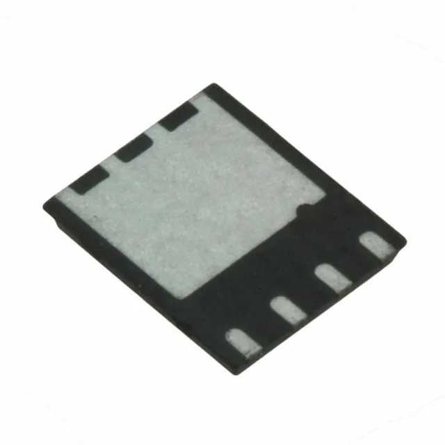
PQFN 5X6 mm
Absolute Maximum Ratings
Max.
Units
VDS
Drain-to-Source Voltage
Parameter
30
V
VGS
± 20
ID @ TA = 25°C
Gate-to-Source Voltage
Continuous Drain Current, VGS @ 10V
ID @ TA = 70°C
Continuous Drain Current, VGS @ 10V
12
ID @ TC = 25°C
Continuous Drain Current, VGS @ 10V
35
IDM
Pulsed Drain Current
110
PD @TA = 25°C
Power Dissipation
PD @TA = 70°C
Power Dissipation
TJ
Linear Derating Factor
Operating Junction and
TSTG
Storage Temperature Range
g
g
15
c
A
W
3.1
2.0
g
W/°C
°C
0.025
-55 to + 150
Thermal Resistance
Parameter
f
RθJC
Junction-to-Case
RθJA
Junction-to-Ambient
g
Typ.
Max.
Units
–––
7.2
°C/W
–––
40
Notes through
are on page 9
1
www.irf.com © 2013 International Rectifier
August 16, 2013
�IRFH7914PbF
Static @ TJ = 25°C (unless otherwise specified)
Parameter
Min. Typ. Max. Units
BVDSS
Drain-to-Source Breakdown Voltage
∆ΒVDSS/∆TJ
RDS(on)
30
–––
–––
Breakdown Voltage Temp. Coefficient
–––
0.022
–––
Static Drain-to-Source On-Resistance
–––
7.5
8.7
–––
11.2
13
V
V/°C Reference to 25°C, ID = 1mA
mΩ
VGS(th)
Gate Threshold Voltage
1.35
1.8
2.35
V
∆VGS(th)
Gate Threshold Voltage Coefficient
–––
-6.08
–––
mV/°C
IDSS
Drain-to-Source Leakage Current
–––
–––
1.0
–––
–––
150
IGSS
Gate-to-Source Forward Leakage
–––
–––
100
Gate-to-Source Reverse Leakage
–––
–––
-100
Forward Transconductance
77
–––
–––
gfs
Qg
Conditions
VGS = 0V, ID = 250µA
µA
nA
S
Total Gate Charge
–––
8.3
12
Qgs1
Pre-Vth Gate-to-Source Charge
–––
2.1
–––
Qgs2
Post-Vth Gate-to-Source Charge
–––
1.0
–––
Qgd
Gate-to-Drain Charge
–––
2.8
–––
Qgodr
Gate Charge Overdrive
Switch Charge (Qgs2 + Qgd)
–––
2.4
–––
Qsw
–––
3.8
–––
Qoss
Output Charge
–––
4.8
–––
nC
RG
td(on)
Gate Resistance
Turn-On Delay Time
–––
–––
1.3
11
2.2
–––
Ω
tr
Rise Time
–––
11
–––
td(off)
Turn-Off Delay Time
–––
12
–––
tf
Fall Time
–––
4.6
–––
Ciss
Input Capacitance
–––
1160
–––
Coss
Output Capacitance
–––
220
–––
Crss
Reverse Transfer Capacitance
–––
100
–––
VGS = 10V, ID = 14A
VGS = 4.5V, ID = 11A
e
e
VDS = VGS, ID = 25µA
VDS = 24V, VGS = 0V
VDS = 24V, VGS = 0V, TJ = 125°C
VGS = 20V
VGS = -20V
VDS = 15V, ID = 11A
VDS = 15V
nC
VGS = 4.5V
ID = 11A
See Fig.17 & 18
VDS = 16V, VGS = 0V
VDD = 15V, VGS = 4.5V
ns
ID = 11A
RG=1.8Ω
See Fig.15
VGS = 0V
pF
VDS = 15V
ƒ = 1.0MHz
Avalanche Characteristics
EAS
Parameter
Single Pulse Avalanche Energy
IAR
Avalanche Current
c
d
Typ.
Max.
Units
–––
17
mJ
–––
11
A
Diode Characteristics
Parameter
IS
Continuous Source Current
ISM
(Body Diode)
Pulsed Source Current
Min. Typ. Max. Units
–––
–––
3.9
A
–––
110
VSD
(Body Diode)
Diode Forward Voltage
–––
–––
–––
1.0
V
trr
Reverse Recovery Time
–––
14
21
ns
Qrr
Reverse Recovery Charge
–––
9.5
14
nC
ton
Forward Turn-On Time
�c
2
Conditions
MOSFET symbol
showing the
integral reverse
D
G
p-n junction diode.
TJ = 25°C, IS = 11A, VGS = 0V
S
e
TJ = 25°C, IF = 11A, VDD = 15V
di/dt = 200A/µs
e�
Intrinsic turn-on time is negligible (turn-on is dominated by LS+LD)
www.irf.com © 2013 International Rectifier
August 16, 2013
�IRFH7914PbF
1000
1000
TOP
ID, Drain-to-Source Current (A)
Tj = 25°C
100
BOTTOM
VGS
10V
5.0V
4.5V
3.5V
3.0V
2.7V
2.5V
2.3V
≤60µs PULSE WIDTH
Tj = 150°C
ID, Drain-to-Source Current (A)
≤60µs PULSE WIDTH
TOP
100
10
1
BOTTOM
VGS
10V
5.0V
4.5V
3.5V
3.0V
2.7V
2.5V
2.3V
10
1
2.3V
2.3V
0.1
0.1
0.1
1
10
100
0.1
V DS, Drain-to-Source Voltage (V)
100
Fig 2. Typical Output Characteristics
1000
2.0
100
TJ = 150°C
10
T J = 25°C
1
VDS = 15V
≤60µs PULSE WIDTH
0.1
ID = 14A
VGS = 10V
1.5
(Normalized)
RDS(on) , Drain-to-Source On Resistance
ID, Drain-to-Source Current (A)
10
V DS, Drain-to-Source Voltage (V)
Fig 1. Typical Output Characteristics
1.0
0.5
1
2
3
4
5
6
VGS , Gate-to-Source Voltage (V)
Fig 3. Typical Transfer Characteristics
3
1
www.irf.com © 2013 International Rectifier
-60 -40 -20 0
20 40 60 80 100 120 140 160
T J , Junction Temperature (°C)
Fig 4. Normalized On-Resistance
vs. Temperature
August 16, 2013
�IRFH7914PbF
14.0
VGS = 0V,
f = 1 MHZ
Ciss = Cgs + Cgd, C ds SHORTED
Crss = Cgd
Ciss
1000
ID= 11A
VGS , Gate-to-Source Voltage (V)
C, Capacitance (pF)
10000
Coss = Cds + Cgd
Coss
Crss
100
12.0
VDS= 24V
VDS= 15V
10.0
8.0
6.0
4.0
2.0
10
0.0
1
10
100
0
2
4
VDS, Drain-to-Source Voltage (V)
1000
ID, Drain-to-Source Current (A)
1000
ISD, Reverse Drain Current (A)
8
10 12 14 16 18 20 22
Fig 6. Typical Gate Charge vs.
Gate-to-Source Voltage
Fig 5. Typical Capacitance vs.
Drain-to-Source Voltage
OPERATION IN THIS AREA
LIMITED BY R DS(on)
100
100
T J = 150°C
10
T J = 25°C
1
100µsec
1msec
10
DC
10msec
1
T A = 25°C
Tj = 150°C
Single Pulse
VGS = 0V
0.1
0.1
0.2
0.4
0.6
0.8
1.0
1.2
1.4
1.6
VSD, Source-to-Drain Voltage (V)
Fig 7. Typical Source-Drain Diode
Forward Voltage
4
6
Q G , Total Gate Charge (nC)
www.irf.com © 2013 International Rectifier
0
1
10
100
VDS, Drain-to-Source Voltage (V)
Fig 8. Maximum Safe Operating Area
August 16, 2013
�IRFH7914PbF
2.5
16
VGS(th) , Gate Threshold Voltage (V)
14
ID, Drain Current (A)
12
10
8
6
4
2
2.0
ID = 25µA
1.5
1.0
0.5
0
25
50
75
100
125
-75 -50 -25
150
0
25
50
75 100 125 150
T J , Temperature ( °C )
T A , Ambient Temperature (°C)
Fig 9. Maximum Drain Current vs.
Ambient Temperature
Fig 10. Threshold Voltage vs. Temperature
Thermal Response ( Z thJA ) °C/W
100
D = 0.50
10
0.20
0.10
0.05
1
τJ
0.02
0.01
R1
R1
τJ
τ1
R2
R2
R3
R3
R4
R4
τA
τ2
τ1
τ2
τ3
τ3
τ4
Ri (°C/W)
τi (sec)
2.0021
0.000245
τA
τ4
Ci= τi/Ri
Ci= τi/Ri
0.1
1E-005
0.0001
0.001
0.014521
15.5002
0.7719
16.4970
38.3
Notes:
1. Duty Factor D = t1/t2
2. Peak Tj = P dm x Zthja + T A
SINGLE PULSE
( THERMAL RESPONSE )
0.01
1E-006
6.0077
0.01
0.1
1
10
100
1000
t1 , Rectangular Pulse Duration (sec)
Fig 11. Maximum Effective Transient Thermal Impedance, Junction-to-Ambient
5
www.irf.com © 2013 International Rectifier
August 16, 2013
�25
80
ID = 14A
EAS , Single Pulse Avalanche Energy (mJ)
RDS(on), Drain-to -Source On Resistance (m Ω)
IRFH7914PbF
20
15
T J = 125°C
10
T J = 25°C
5
ID
3.1A
4.0A
BOTTOM 11A
70
TOP
60
50
40
30
20
10
0
0
2
4
6
8
10 12 14 16 18 20
25
50
75
Fig 12. On-Resistance vs. Gate Voltage
V DS
V GS
+
V
- DD
IAS
20V
RD
D.U.T.
RG
DRIVER
D.U.T
RG
150
Fig 13. Maximum Avalanche Energy
vs. Drain Current
15V
VDS
125
Starting T J , Junction Temperature (°C)
VGS, Gate -to -Source Voltage (V)
L
100
+
-V DD
V10V
GS
Pulse Width ≤ 1 µs
Duty Factor ≤ 0.1
A
0.01Ω
tp
Fig 14a. Unclamped Inductive Test Circuit
V(BR)DSS
tp
Fig 15a. Switching Time Test Circuit
VDS
90%
10%
VGS
td(on)
I AS
Fig 14b. Unclamped Inductive Waveforms
6
tr
td(off)
tf
Fig 15b. Switching Time Waveforms
www.irf.com © 2013 International Rectifier
August 16, 2013
�IRFH7914PbF
D.U.T
Driver Gate Drive
P.W.
+
-
-
-
D.U.T. ISD Waveform
Reverse
Recovery
Current
+
• dv/dt controlled by RG
• Driver same type as D.U.T.
• I SD controlled by Duty Factor "D"
• D.U.T. - Device Under Test
P.W.
Period
*
RG
D=
VGS=10V
Circuit Layout Considerations
• Low Stray Inductance
• Ground Plane
• Low Leakage Inductance
Current Transformer
+
Period
V DD
+
-
Body Diode Forward
Current
di/dt
D.U.T. VDS Waveform
Diode Recovery
dv/dt
Re-Applied
Voltage
Body Diode
VDD
Forward Drop
Inductor Curent
ISD
Ripple ≤ 5%
* VGS = 5V for Logic Level Devices
Fig 16. Peak Diode Recovery dv/dt Test Circuit for N-Channel
HEXFET® Power MOSFETs
Current Regulator
Same Type as D.U.T.
Id
Vds
Vgs
50KΩ
12V
.2µF
.3µF
D.U.T.
+
V
- DS
Vgs(th)
VGS
3mA
IG
ID
Qgs1 Qgs2
Qgd
Qgodr
Current Sampling Resistors
Fig 17. Gate Charge Test Circuit
7
www.irf.com © 2013 International Rectifier
Fig 18. Gate Charge Waveform
August 16, 2013
�IRFH7914PbF
PQFN 5x6 Option "E" Package Details
PQFN Part Marking
INTERNATIONAL
RECTIFIER LOGO
6
DATE CODE
ASSEMBLY SITE CODE
(Per SCOP 200-002)
XXXX
XYWWX
XXXXX
PART NUMBER
MARKING CODE
(Per Marking Spec.)
PIN 1
IDENTIFIER
LOT CODE
(Eng Mode - Min. last 4 digits of EATI #)
(Prod Mode - 4 digits SPN code)
TOP MARKING (LASER)
Note: For the most current drawing please refer to IR website at http://www.irf.com/package/
8
www.irf.com © 2013 International Rectifier
August 16, 2013
�IRFH7914PbF
PQFN Tape and Reel
Note: For the most current drawing please refer to IR website at http://www.irf.com/package/
Notes:
Repetitive rating; pulse width limited by max. junction temperature.
Starting TJ = 25°C, L = 0.27mH, RG = 25Ω, IAS = 11A.
Pulse width ≤ 400µs; duty cycle ≤ 2%.
Rthjc is guaranteed by design
When mounted on 1 inch square 2 oz copper pad on 1.5x1.5 in. board of FR-4 material.
Revision History
Date
08/08/2013
Comments
•�Updated the package drawing, on page 1.
•�Updated the package outline drawing, on page 8.
•�This drawing change is related to PCN "Hana-GTBF-GEM 5x6 PQFN
Public."
IR WORLD HEADQUARTERS: 101 N. Sepulveda Blvd., El Segundo, California 90245, USA
To contact International Rectifier, please visit http://www.irf.com/whoto-call/
9
www.irf.com © 2013 International Rectifier
August 16, 2013
�IMPORTANT NOTICE
The information given in this document shall in no
event be regarded as a guarantee of conditions or
characteristics (“Beschaffenheitsgarantie”) .
With respect to any examples, hints or any typical
values stated herein and/or any information
regarding the application of the product, Infineon
Technologies hereby disclaims any and all
warranties and liabilities of any kind, including
without limitation warranties of non-infringement
of intellectual property rights of any third party.
In addition, any information given in this document
is subject to customer’s compliance with its
obligations stated in this document and any
applicable legal requirements, norms and
standards concerning customer’s products and any
use of the product of Infineon Technologies in
customer’s applications.
The data contained in this document is exclusively
intended for technically trained staff. It is the
responsibility of customer’s technical departments
to evaluate the suitability of the product for the
intended application and the completeness of the
product information given in this document with
respect to such application.
For further information on the product, technology,
delivery terms and conditions and prices please
contact your nearest Infineon Technologies office
(www.infineon.com).
WARNINGS
Due to technical requirements products may
contain dangerous substances. For information on
the types in question please contact your nearest
Infineon Technologies office.
Except as otherwise explicitly approved by Infineon
Technologies in a written document signed by
authorized
representatives
of
Infineon
Technologies, Infineon Technologies’ products may
not be used in any applications where a failure of
the product or any consequences of the use thereof
can reasonably be expected to result in personal
injury.
�


 工商网监
湘ICP备2023018690号
工商网监
湘ICP备2023018690号
