IRG7PG35UPbF
IRG7PG35U-EPbF
INSULATED GATE BIPOLAR TRANSISTOR
Features
Low VCE (ON) trench IGBT technology
Low switching losses
Square RBSOA
100% of the parts tested for ILM
Positive VCE (ON) temperature co-efficient
Tight parameter distribution
Lead-free package
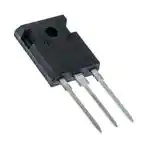
Package Type
IRG7PG35UPbF
IRG7PG35U-EPbF
TO-247AC
TO-247AD
TJ(MAX) = 175°C
G
E
VCE(ON) typ. = 1.9V@ IC = 20A
n-channel
C
C
G
E
GC
G
Gate
C
Collector
IRG7PG35UPbF
IRG7PG35U-EPbF
Max.
1000
55
35
60
80
±30
210
105
-55 to +175
Units
V
A
V
W
°C
300 (0.063 in.(1.6mm) from case)
10 lbf·in (1.1 N·m)
Thermal Resistance
© 2014 International Rectifier
E
Emitter
Orderable Part Number
25
25
Mounting Torque, 6-32 or M3 Screw
Parameter
RθJC (IGBT) Junction-to-Case (IGBT)
RθCS
Case-to-Sink (flat, greased surface)
RθJA
Junction-to-Ambient (typical socket mount)
E
IRG7PG35U-EPbF
TO-247AD
IRG7PG35UPbF
TO-247AC
Tube
Tube
Parameter
Collector-to-Emitter Voltage
VCES
IC @ TC = 25°C
Continuous Collector Current (Silicon Limited)
IC @ TC = 100°C Continuous Collector Current (Silicon Limited)
ICM
Pulse Collector Current, VGE = 15V
ILM
Clamped Inductive Load Current, VGE = 20V
VGE
Continuous Gate-to-Emitter Voltage
PD @ TC = 25°C Maximum Power Dissipation
PD @ TC = 100°C Maximum Power Dissipation
TJ
Operating Junction and
TSTG
Storage Temperature Range
Soldering Temperature, for 10 sec.
www.irf.com
C
Standard Pack
Form
Quantity
Absolute Maximum Ratings
1
VCES = 1000V
IC = 35A, TC = 100°C
Benefits
High efficiency in a wide range of applications
Suitable for a wide range of switching frequencies due to low
VCE(on) and low switching losses
Rugged transient performance for increased reliability
Excellent current sharing in parallel operation
Applications
U.P.S.
Welding
Solar Inverter
Induction heating
Base part number
C
Min.
–––
–––
–––
Typ.
–––
0.24
–––
Submit Datasheet Feedback
Max.
0.70
–––
40
Units
°C/W
April 14, 2014
�IRG7PG35UPbF/IRG7PG35U-EPbF
Electrical Characteristics @ TJ = 25°C (unless otherwise specified)
Parameter
Min.
Typ.
V(BR)CES
Collector-to-Emitter Breakdown Voltage
1000
—
—
1.2
V(BR)CES/TJ Temperature Coeff. of Breakdown Voltage
—
1.9
VCE(on)
Collector-to-Emitter Saturation Voltage
—
2.3
—
2.4
VGE(th)
Gate Threshold Voltage
3.0
—
—
-16
VGE(th)/TJ Gate Threshold Voltage temp coefficient.
gfe
Forward Transconductance
—
22
ICES
Collector-to-Emitter Leakage Current
—
2.0
—
2000
IGES
Gate-to-Emitter Leakage Current
—
—
Switching Characteristics @ TJ = 25°C (unless otherwise specified)
Parameter
Min.
Typ.
Qg
Total Gate Charge
—
85
Qge
Gate-to-Emitter Charge
—
15
Qgc
Gate-to-Collector Charge
—
35
Eon
Turn-On Switching Loss
—
1060
Eoff
Turn-Off Switching Loss
—
620
Etotal
Total Switching Loss
—
1680
td(on)
Turn-On delay time
—
30
tr
Rise time
—
15
td(off)
Turn-Off delay time
—
160
tf
Fall time
—
80
Eon
Turn-On Switching Loss
—
1880
Eoff
Turn-Off Switching Loss
—
1140
Etotal
Total Switching Loss
—
3020
td(on)
Turn-On delay time
—
25
tr
Rise time
—
20
td(off)
Turn-Off delay time
—
200
tf
Fall time
—
200
Cies
Input Capacitance
—
1940
Coes
Output Capacitance
—
60
Cres
Reverse Transfer Capacitance
—
40
RBSOA
Reverse Bias Safe Operating Area
Max. Units
Conditions
—
V
VGE = 0V, IC = 100µA
—
V/°C VGE = 0V, IC = 1.0mA (25°C-150°C)
2.2
IC = 20A, VGE = 15V, TJ = 25°C
—
V IC = 20A, VGE = 15V, TJ = 150°C
—
IC = 20A, VGE = 15V, TJ = 175°C
6.0
V
VCE = VGE, IC = 600µA
—
mV/°C VCE = VGE, IC = 600µA (25°C-150°C)
—
S
VCE = 50V, IC = 20A, PW = 30µs
100
µA
VGE = 0V, VCE = 1000V
—
VGE = 0V, VCE = 1000V, TJ = 175°C
±100
nA VGE = ±30V
Max. Units
Conditions
—
IC = 20A
nC VGE = 15V
—
VCC = 600V
—
—
µJ
IC = 20A, VCC = 600V, VGE = 15V
—
—
RG = 10, L = 200µH, TJ = 25°C
Energy losses include tail & diode
—
ns
reverse recovery
—
Diode clamp the same as
—
IRG7PH35UDPbF
—
—
µJ
IC = 20A, VCC = 600V, VGE = 15V
—
—
RG = 10, L = 200µH, TJ = 175°C
Energy losses include tail & diode
—
ns
reverse recovery
—
Diode clamp the same as
—
IRG7PH35UDPbF
—
—
VGE = 0V
pF VCC = 30V
—
f = 1.0Mhz
—
TJ = 175°C, IC = 80A
FULL SQUARE
VCC = 800V, Vp ≤ 1000V
Rg = 10, VGE = +20V to 0V
Notes:
VCC = 80% (VCES), VGE = 20V, RG = 10.
Pulse width limited by max. junction temperature.
Refer to AN-1086 for guidelines for measuring V(BR)CES safely.
R is measured at TJ of approximately 90°C.
2
www.irf.com
© 2014 International Rectifier
Submit Datasheet Feedback
April 14, 2014
�IRG7PG35UPbF/IRG7PG35U-EPbF
45
For both:
Duty cycle : 50%
Tj = 150°C
Tc = 100°C
Gate drive as specified
Power Dissipation = 70W
40
Load Current ( A )
35
30
25
20
Square Wave:
VCC
15
I
10
Diode as specified
5
0
0.1
1
10
100
f , Frequency ( kHz )
Fig. 1 - Typical Load Current vs. Frequency
(Load Current = IRMS of fundamental)
60
250
50
200
Ptot (W)
IC (A)
40
30
20
10
150
100
50
0
25
50
75
100
125
150
0
175
0
25
50
TC (°C)
75
100
125
150
175
TC (°C)
Fig. 3 - Power Dissipation vs.
Case Temperature
Fig. 2 - Maximum DC Collector Current vs.
Case Temperature
100
1000
10 µs
100
IC (A)
IC (A)
10
100 µs
1
10
1ms
DC
0.1
1
1
10
100
1000
10000
V CE (V)
Fig. 4 - Forward SOA
TC = 25°C, TJ ≤ 175°C; VGE = 15V
3
www.irf.com
© 2014 International Rectifier
10
100
1000
10000
VCE (V)
Fig. 5 - Reverse Bias SOA
TJ = 175°C; VGE = 20V
Submit Datasheet Feedback
April 14, 2014
�IRG7PG35UPbF/IRG7PG35U-EPbF
80
80
VGE = 18V
VGE = 15V
70
VGE = 12V
VGE = 10V
VGE = 8.0V
50
VGE = 18V
VGE = 15V
VGE = 12V
60
VGE = 10V
VGE = 8.0V
50
ICE (A)
60
ICE (A)
70
40
40
30
30
20
20
10
10
0
0
0
2
4
6
8
10
0
2
4
VCE (V)
8
VGE = 18V
VGE = 15V
VGE = 12V
VGE = 10V
VGE = 8.0V
60
50
7
6
VCE (V)
70
ICE (A)
10
Fig. 7 - Typ. IGBT Output Characteristics
TJ = 25°C; tp = 30µs
80
40
30
5
ICE = 10A
ICE = 20A
4
ICE = 40A
20
3
10
2
0
0
2
4
6
8
1
10
4
8
12
16
Fig. 9 - Typical VCE vs. VGE
TJ = -40°C
Fig. 8 - Typ. IGBT Output Characteristics
TJ = 175°C; tp = 30µs
8
7
7
6
6
ICE = 10A
5
5
ICE = 40A
VCE (V)
8
ICE = 10A
ICE = 20A
ICE = 40A
4
20
VGE (V)
VCE (V)
VCE (V)
8
VCE (V)
Fig. 6 - Typ. IGBT Output Characteristics
TJ = -40°C; tp = 30µs
ICE = 20A
4
3
3
2
2
1
1
5
10
15
20
VGE (V)
Fig. 10 - Typical VCE vs. VGE
TJ = 25°C
4
6
www.irf.com
© 2014 International Rectifier
5
10
15
20
VGE (V)
Fig. 11 - Typical VCE vs. VGE
TJ = 175°C
Submit Datasheet Feedback
April 14, 2014
�IRG7PG35UPbF/IRG7PG35U-EPbF
4000
70
3000
60
50
Energy (µJ)
IC, Collector-to-Emitter Current (A)
80
40
TJ = 175°C
30
EON
2000
EOFF
20
1000
TJ = 25°C
10
0
0
4
5
6
7
8
9
10
0
10
20
Fig. 12 - Typ. Transfer Characteristics
VCE = 50V; tp = 30µs
40
Fig. 13 - Typ. Energy Loss vs. IC
TJ = 175°C; L = 680µH; VCE = 600V, RG = 10; VGE = 15V
3500
1000
tdOFF
3000
EON
tF
100
2500
Energy (µJ)
Swiching Time (ns)
30
IC (A)
VGE, Gate-to-Emitter Voltage (V)
tdON
2000
EOFF
1500
10
tR
1000
500
1
0
10
20
30
0
40
IC (A)
Fig. 14 - Typ. Switching Time vs. IC
TJ = 175°C; L = 680µH; VCE = 600V, RG = 10; VGE = 15V
10000
20
40
60
80
100
RG ()
Fig. 15 - Typ. Energy Loss vs. RG
TJ = 175°C; L = 680µH; VCE = 600V, ICE = 20A; VGE = 15V
10000
1000
Capacitance (pF)
Swiching Time (ns)
Cies
tdOFF
tF
100
1000
100
Coes
tdON
tR
10
0
Cres
10
20
40
60
80
100
0
100
200
300
400
500
600
RG ()
VCE (V)
Fig. 16 - Typ. Switching Time vs. RG
TJ = 175°C; L = 680µH; VCE = 600V, ICE = 20A; VGE = 15V
Fig. 17 - Typ. Capacitance vs. VCE
VGE= 0V; f = 1MHz
5
www.irf.com
© 2014 International Rectifier
Submit Datasheet Feedback
April 14, 2014
�IRG7PG35UPbF/IRG7PG35U-EPbF
VGE(th), Gate Threshold Voltage (Normalized)
VGE, Gate-to-Emitter Voltage (V)
16
14
VCES = 600V
VCES = 400V
12
10
8
6
4
2
0
0
20
40
60
80
1.0
IC = 600µA
0.8
0.6
0.4
100
25
50
75
100
125
150
175
Q G, Total Gate Charge (nC)
TJ , Temperature (°C)
Fig. 18 - Typical Gate Charge vs. VGE
ICE = 20A
Fig. 19 - Typical Gate Threshold Voltage
(Normalized) vs. Junction Temperature
1
Thermal Response ( Z thJC )
D = 0.50
0.20
0.1
0.10
0.05
J
0.02
R1
R1
J
1
R3
R3
1
2
2
3
3
SINGLE PULSE
( THERMAL RESPONSE )
0.001
1E-006
1E-005
0.0001
R4
R4
C
Ci= iRi
Ci= iRi
0.01
0.01
R2
R2
4
4
C
Ri (°C/W)
i (sec)
0.017
0.000013
0.218
0.000141
0.299
0.002184
0.177
0.013107
Notes:
1. Duty Factor D = t1/t2
2. Peak Tj = P dm x Zthjc + Tc
0.001
0.01
0.1
t1 , Rectangular Pulse Duration (sec)
Fig. 20 - Maximum Transient Thermal Impedance, Junction-to-Case (IGBT)
6
www.irf.com
© 2014 International Rectifier
Submit Datasheet Feedback
April 14, 2014
�IRG7PG35UPbF/IRG7PG35U-EPbF
L
L
VCC
DUT
0
80 V +
DUT
-
1K
Vclamped
Rg
Fig.C.T.2 - RBSOA Circuit
Fig.C.T.1 - Gate Charge Circuit (turn-off)
C force
DIODE CLAMP
L
100K
D1
22K
C sense
DUT /
DRIVER
VCC
0.0075µ
G force
DUT
Rg
E sense
E force
Fig.C.T.3 - Switching Loss Circuit
7
www.irf.com
© 2014 International Rectifier
Fig.C.T.4 - BVCES Filter Circuit
Submit Datasheet Feedback
April 14, 2014
�IRG7PG35UPbF/IRG7PG35U-EPbF
tf
600
90% ICE
V C E (V)
500
400
300
200
5% ICE
0
-100
-0.5
Eoff Loss
0.5
35
700
30
600
25
500
20
400
15
5% VCE
100
800
200
5
100
0
0
-5
1.5
Fig. WF1 - Typ. Turn-off Loss Waveform
@ TJ = 175°C using Fig. CT.3
www.irf.com
© 2014 International Rectifier
80
70
tr
TEST CURRENT
60
50
40
90% test current
300
10
time(µs)
8
VCE (V)
700
40
I C E (A)
800
30
ICE (A)
20
10% test current
5% VCE
10
0
Eon Loss
-100
-0.5
-10
-0.3 -0.1
0.1
0.3
0.5
time (µs)
Fig. WF2 - Typ. Turn-on Loss Waveform
@ TJ = 175°C using Fig. CT.3
Submit Datasheet Feedback
April 14, 2014
�IRG7PG35UPbF/IRG7PG35U-EPbF
TO-247AC Package Outline
Dimensions are shown in millimeters (inches)
TO-247AC Part Marking Information
Notes: This part marking information applies to devices produced after 02/26/2001
EXAMPLE: THIS IS AN IRFPE30
WITH ASSEMBLY
LOT CODE 5657
ASSEMBLED ON WW 35, 2001
IN THE ASSEMBLY LINE "H"
Note: "P" in assembly line position
indicates "Lead-Free"
INTERNATIONAL
RECTIFIER
LOGO
PART NUMBER
IRFPE30
56
135H
57
ASSEMBLY
LOT CODE
DATE CODE
YEAR 1 = 2001
WEEK 35
LINE H
TO-247AC package is not recommended for Surface Mount Application.
Note: For the most current drawing please refer to IR website at http://www.irf.com/package/
9
www.irf.com
© 2014 International Rectifier
Submit Datasheet Feedback
April 14, 2014
�IRG7PG35UPbF/IRG7PG35U-EPbF
TO-247AD Package Outline
Dimensions are shown in millimeters (inches)
TO-247AD Part Marking Information
E X A M P L E : T H IS IS A N IR G P 3 0 B 1 2 0 K D - E
W IT H A S S E M B L Y
LO T C O D E 5657
ASSEM B LED O N W W 35, 2000
IN T H E A S S E M B L Y L IN E "H "
N o te : "P " in a s s e m b ly lin e p o s itio n
in d ic a te s "L e a d - F re e "
PART N U M BER
IN T E R N A T IO N A L
R E C T IF IE R
LO G O
56
035H
57
ASSEM B LY
LO T C O D E
D A TE C O D E
YE A R 0 = 2 0 0 0
W EEK 35
L IN E H
TO-247AD package is not recommended for Surface Mount Application.
Note: For the most current drawing please refer to IR website at http://www.irf.com/package/
10
www.irf.com
© 2014 International Rectifier
Submit Datasheet Feedback
April 14, 2014
�IRG7PG35UPbF/IRG7PG35U-EPbF
Qualification Information†
Industrial
Qualification Level
Moisture Sensitivity Level
TO-247AC
N/A
TO-247AD
Yes
RoHS Compliant
†
Qualification standards can be found at International Rectifier’s web site: http://www.irf.com/product-info/reliability/
††
Applicable version of JEDEC standard at the time of product release.
IR WORLD HEADQUARTERS: 101 N. Sepulveda Blvd., El Segundo, California 90245, USA
To contact International Rectifier, please visit http://www.irf.com/whoto-call/
11
www.irf.com
© 2014 International Rectifier
Submit Datasheet Feedback
April 14, 2014
�