物料型号:
- 名称:TLE 4250 G
- 订购代码:Q67006-A9351
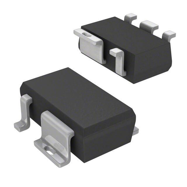
- 封装类型:SCT-595 (SMD)
器件简介:
- TLE 4250 G是一款低功耗电压跟踪器,设计用于汽车电子等恶劣条件下的传感器供电。
- 它具有过载、短路和反极性保护功能。
引脚分配:
- ADJ引脚:调整/使能输入;通过外部电阻或微控制器端口连接到参考电压;高电平激活输入。
- GND引脚:接地;内部连接到引脚5。
- I引脚:输入电压。
- Q引脚:输出电压;必须通过电容Co≥1μF,2≤ESR≤7进行阻断。
参数特性:
- 输出跟踪容差:≤±0.5%
- 输出电流:50 mA
- 工作范围:高达40 V
- 温度范围:-40°C至150°C
- 反向极性保护
- 过温保护
功能详解:
- 通过ADJ引脚跟踪高达40V的供电电压到参考电压。
- 输出能够驱动高达50mA的负载,并且在精度为0.5%的范围内跟随主电压调节器的输出。
- 可通过ADJ引脚将TLE 4250 G切换到待机模式,此时电流消耗极低,适合低功耗电池应用。
应用信息:
- 适用于汽车电子和传感器供电等应用。
封装信息:
- 封装类型为SCT-595,是一种非常小的SMD封装。