Features
Description
The FAN53501 is a step-dow n sw itching voltage
regulator that delivers a fixed 1.82 V from an input voltage
supply of 2.7 V to 5.5 V. Using a proprietary architecture
w ith synchronous rectification, the FAN53501 is capable
of delivering 600 mA at over 90% efficiency, w hile
maintaining a very high efficiency of over 80% at load
currents as low as 1 mA. The regulator operates at a
nominal fixed frequency of 3 MHz at full load, w hich
reduces the value of the external components to 1 µH for
the output inductor and 4.7 µF for the output capacitor.
3 MHz Fixed-Frequency Operation
16 µA Typical Quiescent Current
600 mA Output Current Capability
2.7 V to 5.5 V Input Voltage Range
1.82 V Fixed Output Voltage
Synchronous Operation
Pow er-Save Mode
Soft-Start Capability
Active Discharge During Shutdow n
Input Under-Voltage Lockout (UVLO)
Thermal Shutdow n and Overload Protection
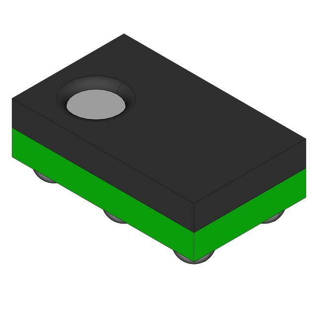
5-Bump - 1.00 x 1.37 mm WLCSP
The FAN53501 is available in a 5-bump Wafer-Level ChipScale Package (WLCSP).
Applications
At moderate and light loads, pulse frequency modulation is
used to operate the device in pow er-save mode w ith a
typical quiescent current of 16µA. Even w ith such a low
quiescent current, the part exhibits excellent transient
response during large load sw ings. At higher loads, the
system automatically sw itches to fixed-frequency control,
operating at 3 MHz. In shutdow n mode, the supply current
drops below 1 µA, reducing pow er consumption.
Cell Phones, Smart-Phones
Pocket PCs
WLAN DC-DC Converter Modules
PDA, DSC, PMP, and MP3 Players
Portable Hard Disk Drives
Ordering Information
Part Number
FAN53501UCX
Operating
Temperature Range
-40°C to 85°C
Package
5-Ball, Type-1, WL-CSP, 1x1.37mm, 0.5mm Pitch
Packing
Method
Tape and Reel
FAN53501AUCX
© 2010 Semiconductor Components Industries, LLC.
October-2017, Rev . 2
Publication Order Number:
FAN53501/D
FAN53501 — 3MHz, 600mA Step-Down DC-DC Converter in Wafer-Level Chip-Scale Packaging
FAN53501
3MHz, 600mA Step-Down DC-DC Converter in
Wafer-Level Chip-Scale Packaging
�4.7µF
VIN
CIN
VIN
A1
A3
B2
EN C1
GND
L1
SW
1µH
C3 FB
VOUT
4.7µF
C OUT
Figure 1. Typical Application, Show n w ith Bum ps Facing Dow n
Block Diagram
VIN
Current Limit
Bias
EN
+
1.8V
Reference
Modulator
Logic
SW
Driver
-
FB
3MHz OSC
Zero Crossing
Figure 2. Block Diagram
GND
Pin Configuration
VIN A1
A3 GND
B2
EN C1
GND A3
SW
SW
FB C3
C3 FB
Figure 3. Bum ps Facing Dow n
A1 VIN
B2
C1 EN
Figure 4. Bum ps Facing Up
Pin Definitions
Pin #
Name
Description
A1
V IN
Pow er Supply Input.
A3
GND
Ground Pin. Signal and pow er ground for the part.
C1
EN
Enable Pin. The device is in shutdow n mode w hen voltage to this pin is 1.2V. Do not leave this pin floating.
C3
FB
Feedback Analog Input. Connect directly to the output capacitor.
B2
SW
Sw itching Node . Connection to the internal PFET sw itch and NFET synchronous rectifier.
www.onsemi.com
2
FAN53501 — 3MHz, 600mA Step-Down DC-DC Converter in Wafer-Level Chip-Scale Packaging
Typical Application
�Stresses exceeding the absolute maximum ratings may damage the device. The device may not function or be operable
above the recommended operating conditions and stressing the parts to these levels is not recommended. In addition,
extended exposure to stresses above the recommended operating conditions may affect device reliability. The absolute
maximum ratings are stress ratings only.
Symbol
Min.
Max.
Unit
Input Voltage w ith Respect to GND
-0.3
6.0
V
Voltage on Any Other Pin w ith Respect to GND
-0.3
V IN
V
TJ
Junction Temperature
-40
+150
°C
TST G
Storage Temperature
-65
+150
°C
+260
°C
V IN
TL
Parameter
Lead Temperature (Soldering, 10 Seconds)
ESD
Electrostatic Discharge
Protection Level
Human Body Model, JESD22-A114
4.5
Charged Device Model, JESD22-C101
1.5
Machine Model, JESD22-A115
200
kV
V
Recommended Operating Conditions
The Recommended Operating Conditions table defines the conditions for actual device operation. Recommended
operating conditions are specified to ensure optimal performance to the datasheet specifications. ON Semiconductor
does not recommend exceeding them or designing to Absolute Maximum Ratings.
Symbol
Parameter
V CC
Supply Voltage Range
IOUT
Output Current
L
Min.
Typ.
Max.
Unit
2.7
5.5
V
0
600
mA
Inductor
0.7
1.0
3.0
µH
Input Capacitor
3.3
4.7
12.0
µF
Output Capacitor
3.3
4.7
12.0
µF
TA
Operating Ambient Temperature
-40
+85
°C
TJ
Operating Junction Temperature
-40
+125
°C
Max.
Units
CIN
COUT
Thermal Properties
Symbol
ΘJA
Parameter
Min.
Junction-to-Ambient Thermal Resistance
(1)
Typ.
180
°C/W
Note:
1. Junction-to-ambient thermal resistance is a function of application and board layout. This data is measured w ith fourlayer 1s2p boards in accordance to JESD51- JEDEC standard. Special attention must be paid not to exceed junction
temperature TJ(max) at a given ambient temperate TA .
www.onsemi.com
3
FAN53501 — 3MHz, 600mA Step-Down DC-DC Converter in Wafer-Level Chip-Scale Packaging
Absolute Maximum Ratings
�Minimum and maximum values are at V IN = 2.7 V to 5.5 V, TA = -40°C to +85°C, CIN = COUT = 4.7 µF, L = 1 µH, unless
otherw ise noted. Typical values are at TA = 25°C, V IN =3.6 V.
Symbol
Parameter
Conditions
Min.
Typ.
Max. Units
Pow er Supplies
IQ
I(SD)
Quiescent Current
Shutdow n Supply Current
V UVLO
Under-Voltage Lockout Threshold
V (ENH)
Enable HIGH-Level Input Voltage
V (ENL)
Enable LOW-Level Input Voltage
I(EN)
Enable Input Leakage Current
Device Not Sw itching, EN=V IN
16
Device Sw itching, EN=V IN
18
25
µA
0.05
1.00
µA
V IN = 3.6 V, EN = GND
µA
Rising Edge
1.8
2.1
Falling Edge
1.75
1.95
1.2
V
V
0.4
V
0.01
1.00
µA
2.5
3.0
3.5
MHz
ILOAD = 0 to 600 mA
1.775
1.820
1.865
V
CCM
1.784
1.820
1.856
V
300
µs
EN = V IN or GND
Oscillator
f 0SC
Oscillator Frequency
Regulation
VO
Output Voltage Accuracy
tSS
Soft-Start
EN = 0 -> 1
Output Driver
RDS(on)
PMOS On Resistance
V IN = V GS = 3.6 V
180
m
NMOS On Resistance
V IN = V GS = 3.6 V
170
m
(2)
ILIM
PMOS Peak Current Limit
Open-Loop
650
800
900
mA
RDIS
Output Discharge Resistance
EN = GND
700
TT SD
Thermal Shutdow n
CCM Only
150
°C
THYS
Thermal Shutdow n Hysteresis
20
°C
Note:
2. The Electrical Characteristics table reflects open-loop data. Refer to Operation Description and Typical Characteristic
for closed-loop data.
www.onsemi.com
4
FAN53501 — 3MHz, 600mA Step-Down DC-DC Converter in Wafer-Level Chip-Scale Packaging
Electrical Characteristics
�The FAN53501 is a step-dow n sw itching voltage
regulator that delivers a fixed 1.82 V from an input voltage
supply of 2.7 V to 5.5 V. Using a proprietary architecture
w ith synchronous rectification, the FAN53501 is capable
of delivering 600mA at over 90% efficiency, w hile
maintaining a light load efficiency of over 80% at load
currents as low as 1 mA. The regulator operates at a
nominal frequency of 3 MHz at full load, w hich reduces
the value of the external components to 1 µH for the
output inductor and 4.7 µF for the output capacitor.
Control Scheme
The FAN53501 uses a proprietary non-linear, fixedfrequency PWM modulator to deliver a fast load transient
response, w hile maintaining a constant sw itching
frequency over a w ide range of operating conditions. The
regulator performance is independent of the output
capacitor ESR, allow ing for the use of ceramic output
capacitors. Although this type of operation normally
results in a sw itching frequency that varies w ith input
voltage and load current, an internal frequency loop holds
the sw itching frequency constant over a large range of
input voltages and load currents.
For very light loads, the FAN53501 operates in
discontinuous current (DCM) single-pulse PFM mode,
w hich produces low output ripple compared w ith other
PFM architectures. Transition betw een PWM and PFM is
seamless, w ith a glitch of less than 14 mV at V OUT during
the transition betw een DCM and CCM modes.
Combined
w ith
exceptional
transient
response
characteristics, the very low quiescent current of the
controller (


 工商网监
湘ICP备2023018690号
工商网监
湘ICP备2023018690号
